

Abstract
We investigate material properties in MoxSi1−x thin films with the goal of optimization for single-photon detection from UV to mid-IR wavelengths. Saturated internal detection efficiency appears to be related to film structure for this material. We demonstrate nanometer-wide meander devices with saturated internal efficiency at 370 nm wavelength and 3.4 K operation temperature. By reducing the film thickness in the optimized material, we demonstrate saturated internal detection efficiency at 1550 nm wavelength and 1 K operation temperature for micron-wide meander shaped single-photon detectors with wire widths up to 2.0 μm and active areas up to 362 × 362 μm2.
Export citation and abstract BibTeX RIS
1. Introduction
Amorphous superconducting materials such as WSi [1], MoSi [2, 3], NbSi [4] and MoGe [5] have been successfully applied to development of superconducting nanowire single-photon detectors (SNSPD). They have shown superior performance in terms of high system detection efficiency of broadband light [6], and recently demonstrated near-unity system detection efficiency [7] in WSi, solving a long controversy on the ability of nanowire detectors to achieve 100% internal detection efficiency. These devices also benefit from high yield fabrication [8] and can be easily integrated with photonic circuits [9, 10] due their amorphous microstructure and deposition at room temperature on a variety of substrates unrestricted by crystalline structure matching. As a result, amorphous based SNSPDs have been employed in a wide range of applications spanning both quantum and classical domain, such as: foundations of quantum mechanics [11], quantum computation [12], molecular spectroscopy [13], integrated photonics [14] and advanced computations [15].
Generally, SNSPD devices consist of nanometer-wide wires that follow a meander design to improve photon coupling and detection efficiency. Recently, there have been new advances both experimentally [16, 17] and theoretically [18] that have demonstrated single-photon sensitivity in wires with micrometer-scale widths. This opened the possibility of scaling up the active area of the detectors from 10 s of μm2 to mm2 while also enabling the use of photolithography instead of electron beam lithography for defining the micron-size device structures. To date, both WSi [19] and MoSi [20] materials have demonstrated saturated internal detection efficiency in micron-size meander devices at 1550 nm wavelength.
However, there are still questions regarding material and device parameters that determine the threshold for single-photon detection and saturated internal detection efficiency for these micron-size meander devices. In addition, extending the broadband detection of single photons from near IR to far IR and terahertz is still an active area of research, and amorphous superconducting detectors are an especially promising system.
In this work we report on a study of Mox Si1−x film optimization for single-photon nanowire devices with saturated internal efficiency at 370 nm wavelength and 3.5 K operation temperature, and for single-photon detection in microwire devices at 1550 nm wavelength and up to 1 K operation temperatures.
2. Mox Si1−x SNSPD devices for enhanced operation temperatures
2.1. Mo0.80Si0.20 thin film structure
Our goal was to make SNSPD devices that operate above 3 K and achieve saturated internal detection efficiency (a plateau of detection efficiency as a function of current bias). We started by optimizing Mox Si1−x film composition and structure for the highest superconducting transition temperature (Tc). Initial evaluation of films (∼50 nm thick) co-sputtered from Mo and Si targets indicated that the highest transition temperature Tc occurred at a composition close to Mo0.80Si0.20, and sharply decreased Tc for compositions with Si less than ∼20 at.% [21].
The first set of devices were fabricated using an alloy target of composition Mo0.80Si0.20 and 99.99 at.% purity. The films were DC magnetron sputtered from a 3'' diameter target on non-heated oxidized Si substrates. Although, the composition was nominally identical (sputtering from an alloy target), we found that the Tc of the films varied with deposition conditions. In order to evaluate the effect of deposition conditions we followed a factorial experiment where Ar sputtering pressure was varied from 1.2 to 3.7 mTorr and sputtering power was varied from 150 to 225 W. The Tc values for ∼50 nm thick films varied from 7.9 K (amorphous films) to 1.3 K (A15 Mo3Si crystalline structure). Table 1 indicates the film deposition conditions, together with the film sheet resistance (Rs) and Tc.
Table 1. Film deposition conditions, sheet resistance (Rs) and Tc values for ∼50 nm film thicknesses.
| Run # | Pressure (mTorr) | Power (W) | RF bias | Film Rs, (Ω/sq) | Tc (K) |
|---|---|---|---|---|---|
| 1 | 2.45 | 225 | Off | 27.47 | 7.86 |
| 2 | 1.23 | 225 | On | 21.84 | 1.52 |
| 3 | 3.67 | 225 | On | 22.61 | 7.9 |
| 4 | 3.67 | 225 | Off | 22.7 | 1.43 |
| 5 | 1.23 | 150 | Off | 37.95 | 1.23 |
| 6 | 2.45 | 225 | On | 21.02 | 1.66 |
| 7 | 3.67 | 150 | On | 28.38 | 1.67 |
| 8 | 1.23 | 150 | On | 27.01 | 1.65 |
| 9 | 3.67 | 150 | Off | 42.72 | 7.75 |
| 10 | 1.23 | 225 | Off | 25.33 | 1.18 |
| 11 | 2.45 | 225 | Off | 27.1 | 1.29 |
We used grazing incidence x-ray diffraction (GIXRD) for evaluation of thin films structure.
No clear trend between deposition conditions (sputtering pressure, sputtering power, RF biasing) and film properties could be extracted from our study for the parameter space explored. We believe this is due to a spontaneous thickness-dependent amorphous to crystalline phase transition which may be associated with stress build-up and surface roughening [22] which affected the long-range atomic order in the films. The film thickness where the phase transition occurred, varied with deposition conditions in no particular trend-following.
To illustrate this thickness-dependent phase transition in the Mo0.80Si0.20 films, we compared the thin film structure evolution for different deposition condition films that exhibited high Tc at ∼50 nm thickness (see table 1). In figure 1 diffraction data indicated that the thin film structure varied with both thickness and deposition conditions.
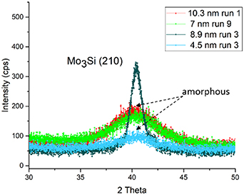
Figure 1. Grazing incidence x-ray scans for different Mo0.80Si0.20 film thicknesses and different deposition conditions illustrated as different run numbers.
Download figure:
Standard image High-resolution imageDepending on deposition conditions, a critical film thickness triggered Mo0.80Si0.20 crystalline phase development. Spontaneous crystallization may transform the entire film thickness (already deposited amorphous layer). As illustrated in figure 1, certain deposition conditions (run 3) that display nominally amorphous structure at 4.5 nm thickness, start showing a crystalline component Mo3Si (210) at ∼9 nm film thickness, whereas other deposition conditions (run 1) continue to maintain amorphous structure above 10 nm.
The amorphous to crystalline transition was correlated with a wide superconducting transition temperature (Tc) band, not suitable for SNSPD device fabrication, as well as Tc degradation—likely due to an increased component of crystalline Mo3Si (210) as indicated in figure 2(b).

Figure 2. (a) Tc measurements for Mo0.80Si0.20 thin films corresponding to deposition conditions identified as run 3 (3.7 mTorr, 225 W). (b) Grazing incidence x-ray diffraction indicating increase of crystalline fraction of Mo3Si (210) with film thickness for the films that also showed a wide transition in (a).
Download figure:
Standard image High-resolution imageThe films analyzed in figure 2, corresponding to deposition conditions identified as run 3 (3.7 mTorr, 225 W), start as nominally amorphous illustrated by the 4.5 nm thick film (figure 2(b)) with a corresponding sharp superconducting transition at Tc= 6.2 K (figure 2(a)). As the film thickness increases to ∼22 nm, the Mo3Si (210) crystalline fraction increases and the superconducting transition broadens significantly. Interestingly, the thickest film, 44.5 nm, displays a sharp transition with a high Tc value of ∼7.9 K, and the x-ray diffraction data indicates a high fraction of amorphous material in addition to some crystalline component.
Due to Tc fluctuations induced by spontaneous phase transformation in Mo0.80Si 0.20 composition films, for certain deposition conditions, we were unable to use a design-of-experiments framework to reliably predict and optimize film's Tc. Instead, we selected deposition conditions that produced thin films with predominantly amorphous structure and sharp Tc, such as the ones identified as run 1 (2.5 mTorr, 225 W) and run 9 (3.7 mTorr, 150 W) in figure 1, and proceeded to fabricate SNSPD meander devices from these films, described in the next section.
2.2. Mo0.80Si0.20 device fabrication and performance
The SNSPD meander geometry was defined with electron-beam lithography using PMMA photoresist and etching was done in SF6 chemistry. We used 6.8 nm thick films Mo0.80Si0.20 capped with 2 nm SiO2. The films displayed a sharp Tc at 6.3 K. We fabricated several meander designs with active areas from 16 × 16 μm2 to 16 × 48 μm2 and wire widths varying from 80 nm to 120 nm. An example of one of the large area devices 16 × 48 μm2 is illustrated in figure 3.

Figure 3. SEM image of Mo0.80Si0.20 SNSPD with and area of 16 × 48 μm2.
Download figure:
Standard image High-resolution imageIn order to test the optical response, the SNSPD devices were cooled down in an adiabatic demagnetization refrigerator and flood illuminated at a wavelength of 370 nm. The devices were tested at both 3.5 K and 300 mK operating temperatures. A room temperature bias tee decoupled the DC bias path from the high-frequency path. The bias current was applied in constant current mode and passed through a series of low-pass filters. The detector signal was amplified at room temperature and fed into a pulse counter. An attenuated 370 nm laser diode was coupled into a standard telecom fiber at room temperature and to the detector via fiber feedthrough.
As shown in figure 4, SNSPD devices with wire widths varying from 80 nm to 120 nm, did not display saturated internal efficiency at 3.5 K and just barely at 300 mK when illuminated with 370 nm wavelength.
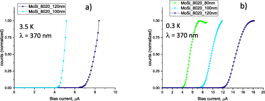
Figure 4. Normalized counts versus bias current for Mo0.80Si0.20 SNSPD devices with 6.8 nm film thickness and Tc of 6.3 K; the curves correspond to different wire widths for the meanders. Under flood-illumination with 370 nm wavelength, the SNSPDs showed non-saturated internal detection efficiency at 3.5 K (a) and just starting to saturate at 300 mK (b) operating temperature. Non-uniform local heating (possibly due to constrictions) in 80 nm wide wire device may result into the dip in counts at high bias. The same device did not display photon response at 3.5 K temperatures.
Download figure:
Standard image High-resolution imageWe also fabricated meander devices from co-sputtered Mo and Si optimized for the highest Tc, with an estimated composition close to Mo0.80Si0.20. Those devices did not indicate saturated internal efficiency, either.
2.3. Mo0.75Si0.25 thin film structure and device performance
Based on our work on Mo0.80Si0.20 and also evidence in the literature [22] that Mox
Si1−x
film crystallization primarily happens at low Si content ( 20 at.%), we explored higher Si compositions such as Mo0.75Si0.25 in both co-sputtering, as well as sputtering from a stoichiometric target with 99.95 at.% purity. Figure 5 shows film Tc variation with thickness for thin films deposited from two stoichiometric targets Mo0.80Si0.20, Mo0.75Si0.25 as well as co-sputtering optimized for highest Tc. The higher Si content is reflected in approximately 1 K lower Tc values for similar film thicknesses.
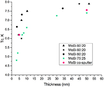
Figure 5. Superconducting transition temperature (Tc) as a function of thicknesses for Mo0.80Si0.20 and Mo0.75Si0.25. Different symbols for Mo0.80Si0.20 (triangle, star and circle) correspond to different deposition conditions identified as run 1, 3 and 9, respectively, in figure 1. Only sharp transitions are indicated in figure 5, so for example for run 3, shown in figure 2, only thicknesses 4.5 nm, 5 nm and 45.5 nm are displayed, the rest of intermediate thicknesses have showed broad transitions, so are not present in this plot.
Download figure:
Standard image High-resolution imageSimilar meander devices, as described in the previous section for the Mo0.80Si0.20 composition, were fabricated out of Mo0.75Si0.25 composition. The films were DC magnetron sputtered from a stoichiometric 3'' diameter alloy target and capped with 2 nm of amorphous Si. X-ray diffraction film measurements indicated an amorphous structure. This time, as shown in figure 6, the SNSPD devices showed saturated detection efficiency under flood illumination with 370 nm wavelength at 3.5 K operation temperature.
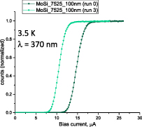
Figure 6. Normalized counts versus bias current for Mo0.75Si0.25 SNSPD devices with 7 nm (run 3: 3.7 mTorr, 225 W) and 8 nm (run 0: 1.2 mTorr, 200 W) film thickness and Tc of ∼6.3 K flood-illuminated with light of 370 nm wavelength; the curves correspond to two different deposition conditions with run 3 corresponding to same deposition conditions used for the Mo0.80Si0.20 SNSPD devices in figure 2. Both SNSPD devices have wire widths of 100 nm.
Download figure:
Standard image High-resolution imageIt is worth noting that for the Mo0.75Si0.25 composition, we have also measured saturated detection efficiency at 1550 nm wavelength and the size of the plateau can be easily increased by fabricating devices from thinner films.
Our study on SNSPD devices fabricated from different Mox Si1−x compositions indicates that non-saturated detection efficiency for the lower Si content films, may be correlated to larger size crystallites or higher fraction of crystalline material in Mo0.80Si0.20 compared to Mo0.75Si0.25. To emphasize this we compared the structure of two same thickness films, ∼9 nm thick, sputtered under identical sputtering conditions, from the two alloy targets: Mo0.80Si0.20 and Mo0.75Si0.25. Figure 7 shows GIXRD measurements for the two different composition films. The sharper peak at 2θ = 40° indicates higher crystalline content in the Mo0.80Si0.20 film. Our data agrees with previous literature studies that showed that the widest bias window for saturated quantum efficiency is achieved in SNSPDs based on amorphous materials, that exhibit excellent homogeneity due to the absence of grain boundaries, in comparison to polycrystalline materials.
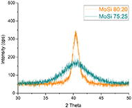
Figure 7. Small crystallites are revealed by GIXRD for two different composition MoSi films with thickness ∼9 nm. Higher crystalline content in Mo0.80Si0.20 as revealed in the sharper peak corresponding to Mo3Si (210). Both films were deposited with the same deposition conditions (run 3).
Download figure:
Standard image High-resolution image3. Mo0.75Si0.25 SNSPD devices with micron-wide wires
Recently, there have been reports of single-photon detection in micron-wide wires [17] as well as SNSPD meander devices with micron-wide wires [19, 20]. The general understanding for operation of superconducting single-photon detectors SNSPDs was previously described in the framework of the 'geometric hot spot model' [23], which assumes that single-photon detection occurs only in a superconducting wire with a width comparable to the size of the hot spot, in the range of 50–150 nm. However, a new theoretical approach [18] based on non-equilibrium superconductivity theory, predicts that for wires that can withstand high supercurrents (above 0.7 of depairing current) the detection efficiency may be independent of the width of the wire.
To test our Mo0.75Si0.25 optimized material capability of detecting single photons in micron-wide detector geometries, we have fabricated SNSPD meander devices with two different film thicknesses: 3.2 nm and 2.1 nm and wire widths ranging from 1 μm to 2 μm. The films were magnetron DC sputtered from a 3'' stoichiometric alloy target with an in situ 2 nm amorphous Si cap layer, as described in section 2.3.
Table 2 shows superconducting and electrical properties of different film thicknesses, d. For comparison with film thicknesses used for nanowire devices described in section 2, a 7 nm thick film is added along with the thinner films: 2.1 and 3.2 nm thick, used in fabrication of the microwire devices. The critical temperature Tc is defined as the middle of the transition where the resistance R(T) = R20K/2, and R20K is the resistance at 20 K. The sheet resistance Rs was measured with a four-probe measurement at room temperature. R20K/R295K is the inverse of the residual-resistance ratio. The diffusion coefficient D was extracted from the temperature dependence of the upper critical magnetic field of our thin films. Measurement details for diffusion coefficient can be found in [24].
Table 2. Superconducting and electrical properties of the Mo0.75Si0.25 thin films.
| d (nm) | Tc (K) | Rs (Ω/sq) | R20K/R295K | D (cm2 s−1) |
|---|---|---|---|---|
| 2.1 | 3.3 | 1015.26 | 1.11 | 0.48 |
| 3.2 | 4.8 | 525.76 | 1.07 | 0.67 |
| 7 | 6.3 | 222.09 | 1.05 | 0.66 |
The main differences between the nanowire devices described in the previous section and this section, are the thickness of the superconducting films and the active area of the devices. Also, the microwire SNSPD devices are defined using photolithography, whereas the nanowire SNSPD devices described in section 2 were defined by electron beam lithography. An example of the microwire SNSPD device is shown in figure 8. The surface area covered by the meandered detector with 2.0 μm wire width and 50% filling factor is 312 × 312 μm2, in contrast to the size of the SNSPD devices described in the previous section with areas as large as 16 × 48 μm2 and wire widths ranging from 80 nm to 120 nm.

Figure 8. Optical micrograph (and zoom in) for a 2 μm wide meander with 50% filling factor covering an area of 312 × 312 μm2.
Download figure:
Standard image High-resolution imageDevices were first characterized in terms of their superconducting properties by measuring current voltage I–V traces and extracting switching currents. Figure 9 shows an example of an I–V curve for the 2 μm wide-wire meander device.
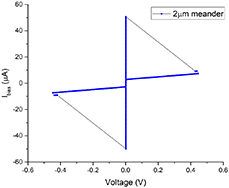
Figure 9. I–V trace, measured at 0.3 K temperature, for 2.1 nm thick meander device with 2 μm wide wires.
Download figure:
Standard image High-resolution imageFor the 2.1 nm thick film meander devices, the switching currents varied from 21 μA to 51 μA for the 1–2 μm wide wires, respectively. For the 3.2 nm thick film meander devices, we measured switching currents from 62 μA to 70 μA for the 1–2 μm wide wires, respectively.
We calculated the theoretical critical depairing current at zero temperature according to the Kupriyanov and Lukichev model [25, 26],

where e is electron charge, N(0) = 1/(2eDρn) is the single-spin electron density of states at Fermi level in the normal state, Δ(0) = 1.764 kB Tc is the superconducting gap at zero temperature, D is the diffusion coefficient, ρn normal state resistivity and w and d are the width and thickness of the nanowire/microwire, respectively.
We found the ratio between the switching current extracted from the I–V curves and the estimated critical depairing current to be in the range 0.50–0.62 for the 2.1 nm devices, and 0.43–0.50 range for the 3.2 nm devices.
To evaluate the photon detection performance of the microwire meanders we flood illuminated the devices with 1550 nm attenuated laser light. Figure 10 shows photon counting performance for several detector geometries corresponding to wire widths of 1, 1.5 and 2 μm and fill fraction of 30%, for the 2.1 nm thick devices. All devices show saturated internal detection efficiency.
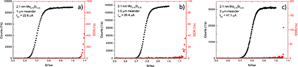
Figure 10. Photon counts rates as a function of the relative bias current taken at 300 mK, for the 1 μm, 1.5 μm and 2 μm wide-wire meanders. All three devices show saturated internal detection efficiency at 1550 nm wavelength and detector areas up to 362 × 362 μm2.
Download figure:
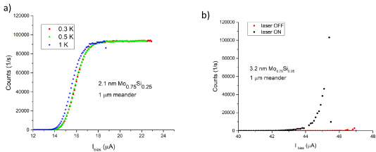
Standard image High-resolution imageWe also measured the count rates as a function of bath temperature and figure 11(a) shows the effect of temperature on the size of the plateau (saturated count rate), for 1 μm wide meander device from 0.3 K to 1 K operating temperatures.
Figure 11. Variation of count rates (a) as a function of bath temperature for 1 μm wide wire meander from 2.1 nm thick film. (b) Count rates as a function of bias at 0.3 K bath temperature for 1 μm wide wire meander from a 3.2 nm thick film; the switching current from I–V curves was 54.5 μA for this device.
Download figure:
Standard image High-resolution image
In contrast with the 2.1 nm thick film devices, the slightly thicker 3.2 nm films did not show saturated internal detection efficiency in micron-wide wire meanders with 1550 nm illumination. Figure 11(b) shows counts vs current bias for 3.2 nm thick meander devices with 1 μm wide wires at 0.3 K. All the other meander devices with wider wires (1.5 and 2 μm), did not show any photoresponse. The photoresponse of the 1 μm wide-wire devices from the 3.2 nm thick film indicates non-saturated internal detection efficiency.
Since the ratio of switching currents to the depairing currents only showed a slight advantage for the 2.1 nm thick film devices compared to the 3.2 nm thick film devices, we looked into other material and device parameters for understanding the differences in detection efficiency. We extracted values of the single-spin electron density of states at Fermi level in the normal state using N(0) = 1/(2eDρn) where e is the electron charge, D is the diffusion coefficient and ρn is the normal film resistivity, respectively. Table 3 shows the values of N(0) calculated based on the above material parameters.
Table 3. Superconducting and electrical properties inferred for the Mo0.75Si0.25 SNSPD devices.
| d (nm) | Tc (K) | ρn(T> Tc) (μΩ m) | D (cm2 s−1) | N(0) (m−3 K−1) | Hot spot radius (nm) | ξ coherence length (nm) |
|---|---|---|---|---|---|---|
| 2.1 | 3.3 | 2.37 | 0.48 | 2.36 1024 | 105 | 8 |
| 3.2 | 4.8 | 1.8 | 0.67 | 2.23 1024 | 59 | 7.7 |
| 7 | 6.3 | 1.64 | 0.66 | 2.49 1024 | 29 | 6.8 |
One of the important phenomena in the photon detection process is the formation of a normal hot-spot of sufficient size which could further translates into a normal belt across wires after photon absorption. We estimated the radius of the normal hot-spot, RNS, based on the formula in (2) that was theoretically [18] derived in the normal-spot model that ignores current-crowding effect and position dependence of detection current, as:
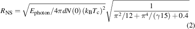
where Ephoton is the absorbed photon energy, d is the film thickness, N(0) is the single-spin electron density of states at the Fermi level in the normal state, kB is the Boltzmann constant, Tc is the superconducting transition temperature and γ is a material parameter (proportional with the ratio of electron Ce and phonon Cph heat capacities taken at T = Tc) that controls the fraction of the photon's energy that gets transferred into the electronic system. The larger the γ is, the larger fraction of incoming energy goes to the electron system. We used γ = 83 for the hot spot radius estimation in (2), which is based on Nion = 1.71 × 1022 cm−3 for Mo0.75Si0.25 (calculated with molar mass of 315.9 g mol−1 and a density of 8.96 g cm−3 [27]) and Ce/Cph = 5.21. For comparison, the WSi values estimated in [18] are γ = 89 and Ce/Cph = 5.65.
The calculated values for the normal hot spot radius displayed in table 3 indicate that for incoming radiation of 1550 nm wavelength (0.8 eV), the size of the spot for the 2.1 nm thick film is almost double compared to the 3.2 nm thick film and is more than three times larger than in the 7 nm thick films. The zero temperature coherence lengths ξ extracted from the magnetic field measurements are also displayed in table 3. For comparison with a different material system: for NbN nanowire detector it was found an estimated [18] hot spot radius of RNS ∼ 26 nm (γ = 9) predicting saturated efficiency in 100 nm wide wire with Idet/Idep ∼ 0.5.
Materials with a small superconducting energy gap and lower density of states are expected to favor high detection efficiency of low-energy photons in SNSPDs. This translates to wide-wire SNSPD devices and it appears that by decreasing film thickness and consequently lowering the film Tc, for a homogeneous material such as Mo0.75Si0.25, the normal hot spot size increases until it reaches an optimum size allowing for subsequent normal belt formation across micron-size wire.
Although saturated efficiency at 5 μm wavelength in 30 nm widths MoSi SNSPDs has been demonstrated [28], another way of increasing detection efficiency of low-energy photons and possibly expand the width of microwire SNSPD devices is to achieve smaller gap and lower density of states by increased content of Si in Mox Si1−x material, similar to behavior observed in Wx Si1−x films [29].
4. Conclusion
In conclusion, we have studied the effect of Mox Si1−x film structure and composition on SNSPD device performance. Mox Si1−x is a versatile material system that can be used for nanowire devices with high detection efficiency optimized from UV to near IR wavelengths, as well as large area devices with micron-wide wires operating with saturated internal efficiency at 1550 nm wavelengths. Optimizing the film structure for increased amorphous fraction ensures optimum detection efficiency.