

Abstract
We confirmed the effectiveness of light-trapping by forming concentric grating couplers (CGCs) inside a transparent sheet. A portion of the light incident to the CGCs is input-coupled and converted to the guided mode and is radiated from neighboring CGCs at a wider angle than the incident angle or even over the critical angle for both surfaces of the sheet. We demonstrated that three stacked sheets with multi-layered CGCs can trap an average of 19%–29% of the incident light at angles of 0° to ±70° in the visible spectrum.
Export citation and abstract BibTeX RIS

Content from this work may be used under the terms of the Creative Commons Attribution 4.0 license. Any further distribution of this work must maintain attribution to the author(s) and the title of the work, journal citation and DOI.
Since light radiates in all directions from a point source, it is difficult to trap it in a small area. 1,2) If a transparent sheet were able to both trap and transport light, it could be used as a solar concentrator and the cost of photovoltaic power is reduced by attaching solar cells to the sheet's edges.
It is already known that a luminescent solar concentrator 3–8) (LSC) can trap a portion of the fluorescence within a plate. The phenomenon of light-trapping must involve an irreversible light-path, and in the LSC, fluorescence distorts the reversibility. Fluorescent light excited by incident light is radiated evenly in all directions from fluorescent dye molecules (or inorganic ions). Components exceeding the critical angle α of the transparent plate are trapped by total internal reflection and travel in a straight line until they are scattered or absorbed by other molecules. The trapping efficiency (TE) of the LSC is η‧cosα (≈ 0.75η) where η is the quantum efficiency of luminescence. However, TE is low due to the limitations of quantum efficiency and the absorption range is confined to narrow spectra. Worse, the transport losses are considerable due to the absorption by the matrix, dyes, and the self-absorption effect 5,6) caused by overlapping of the absorption spectrum and the emission spectrum. Furthermore, when using organic dye molecules, the lifespan of the materials needs to be improved for practical applications. 8)
Other ideas to trap light have also been demonstrated. For example, if a linear-shaped grating is focused and input on the plate's surface and a light beam is aimed at the edge of the grating pattern, a portion of the diffracted light enters the interior and can travel in the plate in guided mode. 9–13) However, the incident angle is limited to a particular value based on a specific wavelength, and the trapped light is emitted to the outside through the same structure as the input structure due to the reciprocity theorem. 14)
Another proposition 15) which gives better transportation performance as a light guide plate than the grating coupler method, uses a volume hologram, 16,17) in which the Bragg diffraction light transports in total internal reflection mode. However, the incident angle and wavelength are also limited to a specific range and strategies to widen the wavelength range cause significant degradation of TE.
If light can be trapped with high efficiency without such limits, optical technologies should see major advances in areas such as concentrating photovoltaic (CPV) technology. 18–21) We devised a novel structure for trapping light and experimentally analyzed it to demonstrate its light-trapping principle.
Figures 1(a)–1(c) show, using a perspective illustration, the structure and operational principle of light-trapping sheets (LTSs), including with concentric grating couplers (CGCs). LTSs are used in a stack, built of CGCs with different specifications. Figures 1(d)–1(f) show scanning electron microscope photographs of the cross-section and surface of CGCs. As shown in Fig. 1d, the LTS is formed by sandwiching a CGC's coupling layers between a quartz substrate (0.625 mm thick) and a planarizing layer made of silicon oxide (3 μm thick). One surface of the quartz substrate is formed into concentric gratings by electron lithography, centering on the centers of the honeycomb pattern, as shown in Fig. 1(f) before the deposition process. The CGCs are comprised of multiple paired layers of a guiding layer (tantalum oxide) and a buffer layer (silicon oxide) on the grating surface. These paired layers are formed with a triangular cross-section due to the self-healing effect of the auto-cloning process. 22) The stacked tantalum oxide layers with gratings work as a grating coupler with high coupling efficiency, and guided light repeatedly undergoes coupling, directional coupling, and radiation between each layer. 23) As shown in Fig. 1(c), light incident on a CGC excites guided light propagating from the center of the input-side CGC to a neighboring CGC. The guided light is radiated above and below from the neighboring CGC over a wider angle than the incident angle (we term this the "wider-angle effect"), and a portion of the radiated light becomes trapped light due to its exceeding the critical angle of the sheet surface.

Fig. 1. (Color online) Structure and operational principle of LTSs. (a) Perspective view of stacked LTSs, (b) perspective view of CGCs formed in an LTS, (c) perspective view showing the relationship between incident light and radiated light. Light incident on a CGC excites guided light, which is radiated from the neighboring CGC. A portion of the radiated light is transported to the sheet edges and is detected by the attached solar cells. (d) and (e) SEM photograph of cross-sections of CGC, which is built by layering multiple paired-layers of a guiding layer (Ta2O5 layer) and a buffer layer (SiO2 layer) on the grating surface. (f) SEM photograph of the surface of CGC.
Download figure:
Standard image High-resolution imageWhy is the radiation angle from the CGC wider than the incident angle ? It is understood theoretically by referring to a propagation diagram. Figure 2(a) shows a two-dimensional (2D) plan of CGCs and Figs. 2(b) and 2(c) show 2D and 3D propagation diagrams of input- and output-coupling by the CGCs, respectively. As shown in Fig. 2(a), the CGCs are located on the x–y plane and are formed inside the honeycomb geometry by concentric circular gratings of period Λ centering on the honeycomb center A and B. Since the excitation of guided light of wavelength λ and wavenumber κ (= 2π/λ) by input-coupling to the CGC-A is limited to the direction where the grating period becomes homogeneous, the guided light vector  1 runs outward from the center A towards its neighbor CGC-B. The vector
  2 is defined as a mirror vector of
  1 about the intermediated plane between A and B to estimate the radiation of light propagated from the CGC-B on the side of the CGC-A. In Figs. 2(b) and 2(c), all circles or a spherical surface of radius r = κ, r = κ‧n0 and r = κ‧neff (where n0 is the refractive index of the sheet, and neff is the effective index of guided light) center on origin point O of the coordinate system of the wave vector (β
x
, β
y
, β
z
). Points R and R0 are located on the circle of r = κ‧neff, and P' and Q' are located on the spherical surface of r = κ‧n0. The vectors
1 about the intermediated plane between A and B to estimate the radiation of light propagated from the CGC-B on the side of the CGC-A. In Figs. 2(b) and 2(c), all circles or a spherical surface of radius r = κ, r = κ‧n0 and r = κ‧neff (where n0 is the refractive index of the sheet, and neff is the effective index of guided light) center on origin point O of the coordinate system of the wave vector (β
x
, β
y
, β
z
). Points R and R0 are located on the circle of r = κ‧neff, and P' and Q' are located on the spherical surface of r = κ‧n0. The vectors  and
and  correspond to the directions of the input light entering on the CGC-A at an angle of θ1, and the output light radiated from the CGC-B at an angle of θ2. The points P and Q are vertical projections of P' and Q' on the x–y plane, respectively. Whereas R0 and P0 are defined as located on the x-axis, P and P0 are located on the arc C1 of radius κ‧n0
 centering on O, and points Q and P0 are located on the arc C2 of radius
  (the magnitude of the lattice vector) centering on R0. The phase matching condition for input-coupling is expressed by the equation
  o
o
 or
or  = 2π/Λ, and that for output-coupling is expressed as
  = 2π/Λ. These conditions are generally strict, but they become less stringent due to the use of incoherent light or microscopic couplers, and the response of the coupling efficiency also becomes insensitive to differences in both wavelength and incident angle (see supplementary Sect. S1 available online at stacks.iop.org/APEX/14/042006/mmedia). The direction of
  1 may therefore show a certain level of spread or be deflected slightly from the incident direction of
  The directions of
  1 and
1 and  2 correspond respectively to
  and
and  at an angle of φ with the x-axis. If the termination of
  1 moves from R0 to R, that of
  2 moves from P0 to P. If the incident condition changes from P0 to the side of P along the arc C1, the termination of
  2 moves from P0 to the Q side along the arc C2. Since the arc C2 is circumscribed with C1 at P0, radiation angle θ2 becomes wider than incident angle θ1 and this proves theoretically the wider-angle effect.

Fig. 2. (Color online) Propagation diagrams of input- and output-coupling by CGCs. (a) 2D plan of CGCs and guided light vectors, (b) 2D diagram, (c) 3D diagram. The directions of incident, guided, and radiated light are explained in the coordinate system of the wave vector (β x , β y , β z ). The input light enters the CGC-A at an angle of θ1 and the output light is radiated from the CGC-B at an angle of θ2. Radiation angle θ2 becomes wider than incident angle θ1.
Download figure:
Standard image High-resolution imageIf Q is outside the circle of r = κ, the propagation of the radiated light exceeds the critical angle of the sheet surfaces. If CGCs are formed on stacked layers, a portion of light radiated from one layer is incident to the other layers and the wider-angle effect is repeated until the propagating angle exceeds the critical angle. Once this happens, it can maintain a state of exceeding the critical angle during internal reflection because the grating pitch of CGCs is sufficiently small (see supplementary S2). It can therefore be said that light trapped by LTSs also benefits from high-performance light transportation.
Figure 3 comprises diagrams that explain the wider-angle effect computationally by using three-dimensional finite difference time domain 24) (3D-FDTD) simulation, where a perfect matched layer 25) is used as the boundary condition. Figures 3(a) and 3(c) are plane views of the structural distribution of CGCs and an intensity distribution of the x–y plane across z = 0. Figure 3(b) is a cross-sectional structure-distribution superimposing the intensity distribution along the x–z plane across y = 0, where the guiding layer (0.2 μm thick, Ta2O5) with triangular-sectional gratings (0.1 μm deep, period 0.25 μm) is sandwiched by surrounding layers (0.5 μm thick, SiO2). As shown in Figs. 3(b) and 3(c), the S-polarized and continuous light of λ = 600 nm is incident at an angle of 25° to the upper and right-half side, framed by the red line in Fig. 3(c), and the reflected and transmitted light occupies the same area. (P-polarized light also works in the same way as S-polarized light, although their coupling angles and coupling efficiencies are slightly different.)

Fig. 3. (Color online) 3D structural model for analysis and numerical results. (a) Structural distributions of a plane view of CGCs with grating period 0.25 μm. (b) Cross-sectional structure-distribution superimposing the intensity distribution of the x–z plane across y = 0. The guiding layer (0.2 μm thick, Ta2O5) with gratings (0.1 μm deep, period 0.25 μm) is sandwiched by surrounding layers (0.5 μm thick, SiO2). (c) Cross-sectional intensity distributions of the x–y plane across z = 0. The light is incident at an angle of 25° from the upper and right-half side framed by the red line and the reflected and transmitted lights occur from the same area. Incident light excites guided light propagating to the left with a slight angle spread, which is radiated above and below from the left-half side. (d)–(g) Far-field patterns inside the silicon oxide medium. The radiated light spread more widely to the outer angle side than the incident light.
Download figure:
Standard image High-resolution imageThe incident light excites the guided light propagating to the left with a slight angle spread, which is then radiated upwards and downwards from the left-half side. Figures 3(d)–3(g) show far-field patterns inside the silicon oxide medium, corresponding to reflective light, transmitted light, upper radiated light, and lower radiated light, respectively. While the patterns of Figs. 3(d) and 3(e) spread as narrowly as that of the incident light, those of Figs. 3(f) and 3(g) spread wider to the outer angle side. This is similar to the relationship between the arc C2 and the point P0 (or P) as shown in Figs. 2(b) and 2(c). These results fully match the above theoretical prediction. The far-field components along the negative abscissa-axis for Figs. 3(f)–3(g) can be ignored because they are generated by diffraction of the left boundary of the incident light and fade away on separating the monitored area framed by the blue line from the left boundary.
Our structure is designed to trap light within the sheet. This means that trapped light propagates over a long distance, and a large computational region is necessary to accurately calculate the optical characteristics of the sheet. Because the calculation model shown in Fig. 3 did not include the seat structure, a numerical analysis could be achieved. However, analyzing the model including the seat structure far exceeds the limits of computation performance using FDTD. Therefore, we tackled the optimization of the sheet structures not by calculation but by experiments.
We fabricated test samples to optimize LTSs by changing certain specifications, such as honeycomb width w, grating pitch  guiding layer thickness t1, buffer layer thickness t2, pair-layer number N, and grating shape such as circle or hexagon (see supplementary S3). The results of our evaluation showed that we could narrow the range of optimum values, such as w = 3–6 μm, t1 = 0.12–0.25 μm, t2 = 0.46–0.52 μm, N = 2–12, and octadecagon shape (see supplementary S4). The specifications of selected testsamples are shown in Table I. CGCs are formed within a 10 mm square at the center of the quartz substrate measuring 20 × 20 × 0.625 mm. Sample versions of "Linear" and "Lumilass," formed as a conventional coupler of uniformly linear gratings or fluorescent glass (Lumilass-R7, Sumita Optical Glass), are added there for comparison with the other LTSs.
Table I. Specification of LTS samples
| Name | N | t1 (μm) | t2 (μm) | Grating shape | w (μm) | Λ (μm) |
|---|---|---|---|---|---|---|
| LTS-a | 6 | 0.16–0.21 | 0.52 | 18 | 3.087 | 0.19 |
| LTS-b | 12 | 0.14–0.25 | 0.52 | 18 | 4.062 | 0.25 |
| LTS-c | 12 | 0.14–0.25 | 0.52 | 18 | 4.874 | 0.30 |
| LTS-d | 12 | 0.12 | 0.46 | 18 | 5.686 | 0.35 |
| LTS-e | 4 | 0.14–0.20 | 0.52 | 18 | 4.874 | 0.30 |
| LTS-f | 2 | 0.14–0.16 | 0.52 | 18 | 4.874 | 0.30 |
| Linear | 20 | 0.16 | 0.26 | Linear | 5000 | 0.24 |
| Lumilass | Fluorescent glass 20 × 20 × 3 mm | |||||
Figure 4(a) shows a demonstration of light-trapping using a stacked sample on a black board. We can see that the end faces of the sample are bright. We developed an experimental system using irradiation of light from an LED (M530F2, etc., Thorlabs) to measure the TE of samples that are composed of 1–3 stacked LTSs. The measuring equipment shown in Figs. 4(b)–4(d) (see Supplementary S5) determines transmissivity and reflectance by using Detector T and Detector R (S3584-08, Hamamatsu Photonics), while continuously changing the angle incident to the sample by controlling two rotating stages. The light emitted from an LED is focused onto the sample's surface at an incident angle of θ by controlling the stage A (KS401-60, Suruga Seiki). The reflected light is collimated on Detector R built on the stage B (S3584-08, Suruga Seiki) at an angle of θ'. The stage B is controlled to maintain the relation of θ = θ'.
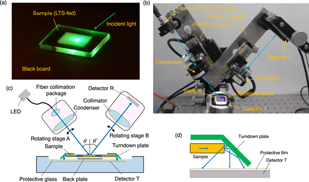
Fig. 4. (Color online) (a) Demonstration of light-trapping using an LTS sample (LTS-fed). The incident light from a green LED is trapped by irradiating the center of the grating pattern. (b) Outside photograph of measuring equipment. The measuring equipment determines the transmissivity and reflectance using Detector T and Detector R, while continuously changing the angle incident to the sample. (c) Configuration diagram of measuring equipment. (d) Cross-sectional drawing showing radiation from the end face of the sample.
Download figure:
Standard image High-resolution imageA back plate like an absorbing plate or a reflective plate is located on Detector T beneath the sample center. The sensitivity of the detectors is calibrated using a semicircular column prism made of BK7 with a diameter of 30 mm. The four sides of the sample are covered by a turndown plate with a square hole of 15 × 15 mm in the middle, whose lower surface is vapor-deposited with aluminum to reflect light radiated from the end face of the sample and bring it to Detector T. Since the size of Detector T is larger than that of the sample (i.e. 28 × 28 mm versus 20 × 20 mm) and the gap between the sample and Detector T is sufficiently narrowed (with a space of 1 mm), light other than reflected light from the sample can mostly fall on Detector T. Thus, TE is estimated from the value detected by Detector T using an absorbing plate as the back plate. Whereas, since the absorbing plate blocks out only the transmitted light, the transmissivity is estimated by subtracting the two values detected by Detector T for whether the absorbing plate is present or absent. The reflectance for diffuse reflection (diffuse reflectance, DR) is estimated from the amount other than the summation of TE and transmissivity. Since we employ an absorbing plate (or a reflective plate) that is narrower than the patterned area and use it to measure only the amount of light that is trapped, a portion of the leaked light may be detected by Detector T on the outside of the absorbing plate and may be filed in the amount of TE, when the proportion of a wavelength to grating pitch is less than about 2.7 (see supplementary S6).
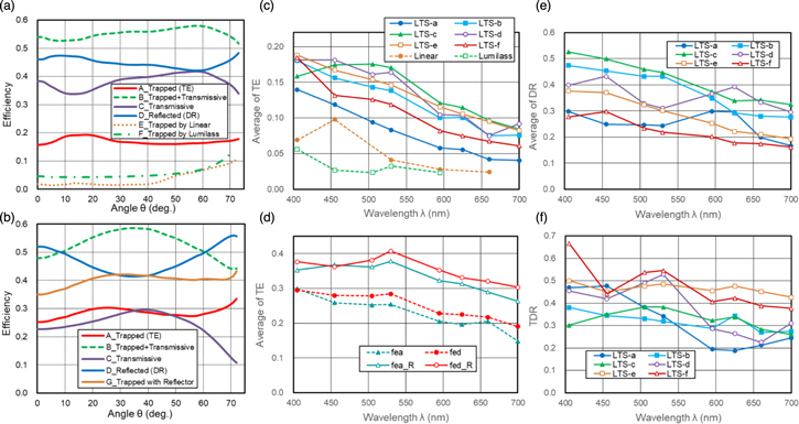
Figures 5(a) and 5(b) show the experimental results for a single LTS (LTS-c) and three stacked LTSs (LTS-fed, i.e. the order of LTS-f, -e, and -d as seen from the irradiated side), respectively. The respective efficiencies are plotted for λ = 530 nm on the vertical axis and incident angle θ on the horizontal axis. In each Figure, the line A shows the results as measured by Detector T using the absorbing plate as the back plate, corresponding to the amount of trapped light. The line B shows the measured result for Detector T with the absorbing plate off, which corresponds to the sum of the trapped light and transmissive light. The lines C and D are calculated by subtracting the line A from the line B and subtracting the line B from 1.0. The line D indicates the reflectance DR, including absorption caused by the setup's materials. The above two Figures reveal that light can be efficiently trapped inside the sheet due to the wider-angle effect and that TEs show gradual changes of 16%–19% and 25%–32% in the range of 0°–72° for a single LTS and three stacked LTSs, respectively. As shown by the curve of G in Fig. 5(b), TE is raised by about 10 % by replacing the absorbing plate with a reflective plate. For reference, the measured result of "Linear" is added to Fig. 5(a). The average TE is below 4% due to a lack of the wider-angle effect, where the light is trapped by diffraction at the stacked layers (not by grating diffraction) because the result for TE measured from the orthogonal direction becomes the same. A measured result for "Lumilass" excited by a violet LED (λ = 405 nm, M405F1, Thorlabs) is also added to Fig. 5(a).
Fig. 5. (Color online) Experimental results for TE and DR. (a) Angular response for LTS-c. Several efficiencies for λ = 530 nm (curves of A–F) are plotted on a vertical axis. The measured result for "Lumilass" excited by a violet LED is added here. (b) Angular response for LTS-fed. Several efficiencies for λ = 530 nm (curves of A–D, and G) are plotted on a vertical axis. LTS-fed is stacked in the order of LTS-f, -e, and -d as seen from the irradiated side. The curve of G is measured by using the reflective plate as the back plate. (c) Wavelength response of TE for a single LTS. The measured results for "Lenear" and "Lumilass" are added here. (d) Wavelength response of TE for three stacked LTSs. The averages of TE are plotted as a parameter for combinations of LTSs. "fea" (or "fed") is stacked in the order of LTS-f, -e, and -a (or LTS-f, -e, and -d). Curves for "fea_R" and "fed_R" are measured by using the reflective plate as the back plate. (e) Wavelength response of DR for a single LTS. The averages of DR are plotted as a parameter for a single LTS. (f) Wavelength response of TDR for a single LTS. TDR is defined as the proportion of the averages of TE and DR.
Download figure:
Standard image High-resolution image
Figures 5(c)–5(e) show the experimental results from plotting wavelength λ on the horizontal axis and the averages of TE and DR on the vertical axis as a parameter with combination of LTSs, respectively. These two efficiencies are averaged over the range of θ = 0°–70°. Measurement errors for the average of TE were about ± 10% of the measured value or ± 0.02 of the absolute error, whichever was greater, at some typical points. For LTS-c, TE is 8%–18% in the range of λ = 405–700 nm, while DR is 32%–53%. As references, the average TE for "Lumilass" is less than 6% at the excitation by a violet LED and it approaches 0% for larger visible wavelengths: the average TE for "Linear" which is listed in Table I as one of previous couplers is about 1/3 of that for LTS-b due to a lack of the wider-angle effect. With three stacked LTSs (LTS-fed), TE is 19%–29% in the range of λ = 405–700 nm. Curves for fed_R are measured by using the reflective plate as the back plate, with which the average TE for fed_R increases by about 10%. The proportion of the two (TD rate or TDR) is 0.26–0.38 for LTS-e or -f, as shown in Fig. 5(f). TDR can increase up to 0.4–0.7 due to reduction of the pair-layer number N as in LTS-a, -e, or -f, or by optimization of thickness t1 and t2 as in LTS-d. We can therefore anticipate maintaining the TDR for visible spectra at a level of above 0.5 by further structural optimization of the LTS. If TE and DR have no angular dependency, the level of TDR for a single LTS theoretically determines the level of TE for stacked LTSs. We have predicted mathematically that TE can potentially be raised to about 60% as a result of stacking LTSs with a high TDR (see supplementary S7).
Our LTS achieved much higher TE compared to the fluorescent glass ("Lumilass") or the previous coupler ("Linear"). Since our principle is subject to a linear process based on Maxwell's equations, unlike fluorescence in fluorescent glass, it has a capacity limitation for light transportation, but it can be improved by adjusting the grating pitch or pair-layer number.
Our measurements showed that the TE increases with shortening wavelength. This is because TE is proportional to the ratio of the grating depth to the wavelength. To improve the TE, it is therefore important to develop a forming process that creates deep gratings for application to stacked layers. Developing a forming process for fine gratings for stacked layers is also important to improve the light-transportation performance.
It is better to stack the LTS of the smaller DR on the irradiated side when aiming to increase the TE. It is also better to trap the shorter wavelengths first when aiming to trap the whole spectrum of sunlight. The stacking sequence of the sheets therefore should be in ascending order of DR or grating-pitch starting from the irradiated side. To be able to apply this technology to concentrating solar photovoltaics, the solar cells attached at the sheet edges should be compound semiconductors that are tuned to the ranges of the trapped wavelengths.
Because our technology requires only minimal investment in materials development and can respond to the full range of the solar spectrum by adopting a combination of grating specifications, we regard this as a breakthrough in CPV technology. We will aim in future to achieve better performance and will at the same time investigate the potential for a low-cost, mass fabrication process.
Acknowledgments
The authors thank T. Nakagawa for providing motivation for the development of devices, M. Kitagawa for providing financial support, B. Mizuno for experimental support, K. Lee for sensor calibration.