


Introduction
Monolithic microwave integrated circuits (MMICs) often require a transition from their planar form to a waveguide in order to effectively couple input and output signals. This is usually achieved through the application of a waveguide-to-microstrip (WG-MS) transition that transforms the impedance of the waveguide channel to the optimal conjugate impedance of the MMIC input or output port. At millimeter wavelengths, the WG-MS transition is typically fabricated from a thin film gold conductive layer, ~3 μm in thickness, which is deposited onto a thin, <100 μm, quartz or alumina substrate and then suitably patterned to form a sequence of distributed elements [Reference Cuadrado-Calle, George, Fuller, Cleary, Samoska, Kangaslahti, Kooi, Soria, Varonen, Lai and Mei1–Reference Samoska3].
Using WG-MS transitions at frequencies higher than 100 GHz presents three particular challenges: (1) due to the uncertainties in pre-packaging on-wafer probing, it is often difficult to determine precisely the optimal impedance required by the MMIC [Reference Sakamaki and Horibe4, Reference Reck, Chen, Zhang, Arsenovic, Lichtenberger, Weikle and Scott Barker5]; (2) simulating the interaction between the MMIC and the WG-MS transition is highly complex and thus prone to error; (3) once installed, the fabricated transition cannot be tuned in order to optimize the device packaged performance, i.e. to correct for the errors that may arise from 1 and 2.
A tuning technique commonly used in planar matching networks at lower frequencies incorporates patch tuning elements to modify transmission line impedances and lengths [Reference Lopez-Fernandez, Gallego Puyol, Diez Gonzalez and Barcia Cancio6–Reference Amils, Gallego, Diez, Lopez Fernandez, Barcia, Muñoz, Sebastian and Malo8]. Unfortunately, this technique cannot readily be implemented at millimeter wavelengths ranges due to the smaller feature size and assembly complexity of the related circuitry. To achieve performance requirements, it is therefore often necessary to assemble (package) and test multiple design variations, and perform a subsequent device selection, or to sequentially disassemble and substitute components. Clearly, these approaches are very inefficient, wasteful, and costly. Additionally, the inherent variability of MMIC performance observed at millimeter wavelengths [Reference Cuadrado-Calle, George, Fuller, Cleary, Samoska, Kangaslahti, Kooi, Soria, Varonen, Lai and Mei1, Reference Reeves, Cleary, Gawande, Kooi, Lamb, Readhead, Weinreb, Gaier, Kangaslahti, Russell, Samoska, Varonen, Lai and Sarkozy9] can affect packaged performance repeatability and often mask the effect of applied changes.
We address the above difficulties through the demonstration of a novel empirical method of circuit tuning that allows the in situ optimization of millimeter-wave packaged device microstrip and coplanar impedance-matching elements. Our approach makes use of laser “machining” to trim the planar interface circuit conductor area and thereby allowing the application of additional inductance and resistance in pre-selected areas of a matching network. Being a subtractive process, it is not possible to add material and this can limit the extent of circuit tuning that is achievable. Whilst laser trimming is already used for electronic component tuning, e.g. thin-film resistor [Reference Boulais, Fantoni, Chateauneuf, Savaria and Meunier10, Reference Sandborn11] and capacitor [Reference Yamaguchi12, 13] parameter adjustment, to the best of our knowledge, it has not previously been applied in the in situ optimization of packaged millimeter-wave MMIC devices. Moreover, we have demonstrated that the modified circuit can be transferred to a conventional photolithographic process and used to reproduce optimized performance in similar devices reliably using fully space-qualified processes. This provides advantages for multiple device production and spaceflight applications.
Methodology
In order to demonstrate our in situ tuning technique, we designed and fabricated a WG-MS output transition suitable for packaging with a state-of-the-art low noise amplifier (LNA) MMIC operating at a center frequency of 183 GHz [Reference Rösch, Tessmann, Leuther, Weber, Moschetti, Aja, Kotiranta, Massler, Kangas, Perichaud, Schlechtweg and Ambacher14, Reference Moschetti, Leuther, Maßler, Aja, Rösch, Schlechtweg, Ambacher, Kangas and Geneviève-Perichaud15] and destined for use in space-borne radiometers aboard the MetOp-SG meteorological satellite series [Reference D'Addio, Kangas, Klein, Loiselet and Mason16, Reference Cuadrado-Calle, Rea, Auriacombe, Oldfield, Parow-Souchon, Obeed, Klugmann, Rackauskas, Davis, Hunyor, Merritt, Phillips, Beardsley, Moyna, Ellison, Thomas, Hammett, Kangas and Piironen17]. The design process was as described in [Reference Leong and Weinreb18]. The WG-MS pre-trimming design was performed using HFSS [19] and optimized to the MMIC output impedance requirements obtained from a previous wafer probe measurement performed by the chip supplier [Reference Rösch, Tessmann, Leuther, Weber, Moschetti, Aja, Kotiranta, Massler, Kangas, Perichaud, Schlechtweg and Ambacher14, Reference Moschetti, Leuther, Maßler, Aja, Rösch, Schlechtweg, Ambacher, Kangas and Geneviève-Perichaud15]. The waveguide channel impedance was ZWG ≈ 489.2 Ohm at 183 GHz. The output impedance of the MMIC was ZMMIC ≈ 120 + 101j Ohm at 183 GHz. The WG-MS transitions were fabricated on a 25 μm-thick quartz substrate with a 3 μm gold conductor layer. Quartz has a dielectric constant (ɛr) of 3.8 [Reference Rösch, Tessmann, Leuther, Weber, Moschetti, Aja, Kotiranta, Massler, Kangas, Perichaud, Schlechtweg and Ambacher14]. Figure 1 shows the original untrimmed transition assembled onto a 183 GHz LNA.

Fig. 1. Original untrimmed WG-MS transition assembled onto a 183 GHz LNA. The quartz dimensions are 941 × 200 × 25 μm. Full MMIC image available in [Reference Moschetti, Leuther, Maßler, Aja, Rösch, Schlechtweg, Ambacher, Kangas and Geneviève-Perichaud15].
A calibrated Keysight vector network analyzer (VNA) N5225B with WR-5 waveguide frequency extenders was installed beside a pulsed frequency tripled neodymium-doped yttrium aluminum garnet (Nd:YAG) laser with an output wavelength of 355 nm and as shown in Fig. 2. The LNA comprised a two-part split mechanical housing that when separated allowed access to the device internal components. All microwave circuitry, including the transitions to be trimmed, were contained in a single half that was placed securely on a high-precision (micrometer accuracy) lateral positioning stage. The stage was located beneath an optical inspection microscope and the laser system and, with the use of an integrated camera, allowed accurate positing of the LNA and dimensional recording of all implemented laser trims. Advanced inspection tools such as scanning electron microscopy imaging were also used upon completion of the “trimming campaign” to validate the initial assessment.

Fig. 2. (a) Laser setup and (b) LNA characterization setup during trimming activity.
Laser settings were incrementally optimized using spare transition samples. For example, variations of scan speed and repetition rate were used to micromachine the surface with the aim of reducing damage to adjacent and underlying areas. An optimum gold ablation threshold was determined by defining points along a feature to be trimmed and setting the number of pulses applied at each point. During this process, gold metallization on the underside of the quartz dielectric was monitored for unwanted laser ablation, which can lead to explosive evaporation of an epoxy layer used to attach the transition, resulting in the destruction of the assembly. Visual inspection using microscopy guided the optimization of the laser settings to produce a minimal effect on the bottom metallization whilst achieving functionally adequate gold removal on the top metallization.
A packaged LNA S-parameter performance was first measured using the VNA and in situ laser trimming applied to the WG-MS area previously identified as most relevant for tuning. Metal was removed with a single 30 ns laser pulse focused to a diameter of 15 μm, and with a fluence of approximately 6 J/cm2. The laser system uses a scanning refractive optic to define the laser cutting area and operational parameters were varied to optimize the ablation of the gold conductor in terms of complete material removal, minimum collateral damage, and sharp edge definition. After each application of laser trimming, the packaged MMIC was re-measured using the VNA. A 15 μm spot size was sufficient for the feature size of the impedance-matching network presented in this paper. However, for other (e.g. higher frequency) matching networks, a better defined focal area might be needed. This can be easily achieved using higher quality focusing optics [Reference Knowles, Rutterford, Karnakis and Ferguson20].
Results
Pre-trimming assessment
The measured output return loss, S22, prior to the trimming campaign was found to be between −10 and −15 dB for frequencies between 175 and 191 GHz. This resulted in standing waves between the LNA output and a post-amplification down-conversion stage in the MetOp-SG space-borne receiver system engineering model [Reference Leong and Weinreb18]. In turn, this introduced a frequency-dependent gain variation and affected sideband balance, leading to a significantly impaired radiometric performance. The downconverter input is a double sideband Schottky barrier diode mixer with a measured input return loss of 8 dB.
Trimming and removal analysis
A single trimming procedure including the laser ablation, microscopic imaging of the WG-MS transition, S-parameter measurement of the LNA block and decision-making took approximately 30 min. The procedure was initially applied to a spare “test device” LNA as a means of empirically understanding the effect of each gold removal action on the S22 of the packaged device (Fig. 3). The trim areas were preselected to provide control over the series inductance, A, shunt capacitance, B, and a combination of inductance and capacitance, C, of the circuit.

Fig. 3. Effect of trimming different areas on the WG-MS transition. The black dot on the Smith chart shows the initial measured S22 of the LNA, at the band center, 183.3 GHz. The letters A, B, and C show different trim areas on the circuit, and the corresponding arrows and shaded regions on the Smith chart show the direction of movement of the impedance as the conductor was removed.
The most effective trim area from an impedance-matching perspective was A, i.e. narrowing the conductor next to the bond to the MMIC. After this initial mapping, a 120 μm-long and 50 μm-wide microstrip line was reduced in width, initially by 11.5 μm (trimming step 1) and subsequently by 15 μm (trimming step 2). Pictures of the transition during the trimming process are shown in Fig. 4. The same figure also shows the initial performance of the LNA with the untrimmed transition (trimming step 0) and the performance improvement of the LNA throughout the trimming process. The magnitude of S22 improved by nearly 19 dB at 178 GHz. The average improvement in the band of interest, 175–191 GHz, was 9.8 dB. The Cartesian plot on Fig. 4 shows that there was no measurable change in the gain of the amplifier after trimming the output transition. The input impedance match, not shown in Fig. 4, was unaffected. The lower S22 reduced the standing wave between the LNA and Schottky mixer such that gain flatness and sideband balance in the receiver were acceptable.
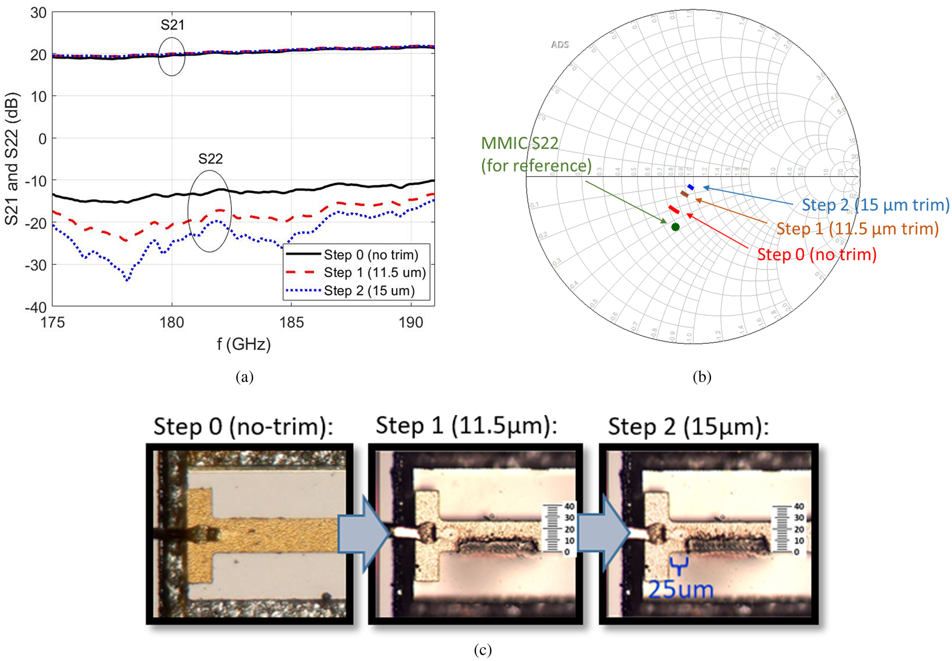
Fig. 4. Trimming process on original LNA. (a) Measured S21 and S22 during each trimming step, in Cartesian format. (b) Measured S22 during each trimming step and S22 of the MMIC chip, from 183.2 to 183.4 GHz, on the Smith chart. (c) Microscopic photographs of performed trimming steps.
Following trimming, the modified areas were analyzed using energy-dispersive X-ray (EDX) imaging. Figure 5 shows the achieved level of gold removal with only some small (area, <<1 μm2) remnants of gold remaining in the area of the trim and on the edge of the ablated copper traces. When compared with the signal wavelength, the very small size of gold particles will have little impact upon the signal transmission of the propagating modes. In addition to gold, the EDX image in Fig. 5 reveals the presence of silicon and oxygen from the fused quartz, SiO2, substrate and a low level, 0.29% of argon, which may arise from the deposition of the gold layer of the transition in a partial argon atmosphere.

Fig. 5. EDX element map and atom abundance of a corner within the trimmed area of the transition.
Reproduction for spaceflight LNAs
As a test of reproducibility, the trimmed transition dimensions were measured, transferred to a photolithographic mask and an equivalent circuit was manufactured. A photograph of the revised structure is shown in Fig. 6. The required performance improvement was exhibited by all LNAs using the new transition: the measured S22 results from two of these new LNAs are shown in Fig. 7. The slightly different shape between the S22 trace of the LNA with the trimmed transition and the S22 trace of the two LNAs with the photographically reproduced transitions is likely due to the superior photolithographic edge definition in the new transition, plus a variation in MMIC performance as previously indicated. The probed S22 of the MMICs inside the original LNA and the two LNAs with the photographically reproduced transitions is also shown in Fig. 7. The MMICs on replicated LNA 1 and replicated LNA 2 feature the same design as those on the original LNA, but are from a different wafer.

Fig. 6. Revised WG-MS transition in all 183 GHz LNAs for MetOp-SG. The modified cut is highlighted. The coplanar output line on the MMIC is to the left of the transition. The waveguide channel is to the right of the transition.

Fig. 7. Measured S21 and S22 of two LNAs with redesigned WG-MS transitions compared with original untrimmed measurements and laser trimmed measurements on original module. Measured S22 of MMICs inside original and replicated LNAs are also shown.
Conclusion
This paper has presented an empirical trimming solution that provides a significant improvement in achieving packaged millimeter-wave device performance and where analytical design methods alone are insufficient. It offers the previously unavailable path of in situ post-fabrication optimization of matching networks, via small incremental changes to the conductor layer, that are impossible to implement using conventional micro-assembly techniques. Moreover, it can in principle be applied to other accessible millimeter-wave circuit elements.
The impact of the laser trimming technique could be further enhanced if performed with in situ S-parameter measurements, i.e. where simultaneous laser trimming and device performance characterization is possible. This would allow the execution of faster and potentially refined circuit tuning. However, this is only possible where removal of the device package cover does not in itself impact performance. For instance, simultaneous measurement and laser trimming of a WG-MS transition as described in this paper would not be possible due to the need to separate the waveguide structure in order to gain laser access.
Finally, it is important to stress that the proposed technique is not a substitute for good initial circuit design. It is an empirical method of affording device optimization through the precision trimming of complex and sensitive millimeter-wave circuity.
Acknowledgement
The development work described here has been performed in support of the Meteorological Operational Satellite – Second Generation (MetOp-SG).
 Kai Parow-Souchon graduated from RWTH Aachen University in Germany in October 2014, after studying electronic engineering with a focus on satellite communications. He then joined the Millimetre Wave Technology Group at the STFC Rutherford Appleton Laboratory and is currently working on millimeter-wave amplifier modules and other RF components to be used in the three millimeter-wave instruments in ESA's MetOp operational meteorology program: MWS, MWI, and ICI, as well as power amplifiers and miniaturized millimeter-wave systems for other projects. Kai's main research interest is optimizing the packaging of millimeter-wave components.
 David Cuadrado-Calle received his B.Sc. and M.Sc. degrees in 2010 and 2012, from the University of Alcala, Spain, and his Ph.D. degree in 2017 from the University of Manchester, UK. In 2011–2012, David was with the Yebes Observatory, Spain. In 2012–2013, he worked as an RF engineer in the private sector. During his Ph.D., 2013–2017, and subsequent post-doc in Manchester, 2017–2018, David designed and developed MMIC LNAs for ESO's ALMA band 2 (67–116 GHz) receiver cartridge. His Ph.D. was partly done at Caltech and NASA's JPL, USA. In 2018, David started a new position as a millimeter-wave engineer at the Rutherford Appleton Laboratory, UK, where he is currently supporting the development of spaceflight receivers for MetOp-SG. David was the recipient of the Royal Astronomical Society's Thesis Prize 2017 to the best Ph.D. thesis of the year in the UK in the area of instrumentation science for astronomy and geophysics.
Simon Rea is head of the Device Design Section within the Millimetre Wave Technology Group at RAL Space, joining the Group in 2009. Prior to his current role, he worked in the Earth Observation, Navigation and Science Department at EADS Astrium. He has been involved in a wide range of projects relating to the analysis, design, and test of passive and active instrumentation for Earth Observation missions at both component and system level. He is an experienced millimeter-wave component designer with significant experience in the design and optimization of Schottky-diode-based components and the packaging of MMIC devices. He also has considerable experience in the design, integration, and testing of millimeter-wave receivers and instruments, including the deployment of instrumentation on ground and airborne platforms. Since April 2015, he has been the Responsible Engineer on a multi-million pound contract to supply millimeter-wave front-end receivers for three instruments on the MetOp Second Generation program, Europe's next-generation operational mission for weather forecasting.
 Manju Henry obtained her Masters and Ph.D. degree in Electronic Engineering from Cochin University of Science and Technology, Kerala, India in 1998 and 2002, respectively. After her Ph.D., she had completed 5 years of post-doctoral studies at the Institute of High Frequency and Microwave Techniques (IHM) at Karlsruhe Institute of Technology, the former FZK, Germany and at the University of Surrey, UK. She joined the MMT Group at Rutherford Appleton Laboratory in 2007. After joining the group, she had undertaken key technical and management roles in several EU/ESA programs. She is currently involved in a wide range of tasks that include millimeter-wave passive system design for atmospheric sounding and astronomy, active system development for meteorological remote sounding and security imaging.
M. Merritt Photograph and biography not available at the time of publication.
 Peter Hunyor holds a BEng (Hons). Certified Airline and Aerospace surface finisher (by NASF (National Association for Surface Finishing) USA). Joined the Science and Technology Facilities Council (STFC) as a process engineer in 2015 and has been working on various surface finishing and inspection techniques ever since. He is managing the gold-plating & electro-forming laboratory and the materials analysis laboratory within the MMT Group. Currently working on the European Space Agency (ESA's) MetOp project where he successfully validated multiple surface finishing processes for flight. His current research interest include additive manufacturing and high precision electroforming to develop corrugated feedhorns.
N. Brewster Photograph and biography not available at the time of publication.
 Lisa Harman has worked in the laser and optics industry since 1997. Prior to joining Scitech Precision, she worked for Micronanics, Exitech, and the Central Laser Facility.
 Chris Spindloe has worked in the laser target field since 2003. He has an interest in thin-film coating, precision assembly, micro-engineering, and the metrology of sub-millimeter components. His current research interests are high rep rate target solutions and developing novel targets for studying matter under extreme conditions.
 Peter Sykes joined Scitech Precision in February 2016. Previously, he has worked in the lasers and optics industry for over 16 years gaining specialist knowledge in the field of laser micro-machining. Peter has previously worked for Micronanics, M-Solv, and Exitech in the laser machining, R&D, and production departments.
 Peter G. Huggard received B.A. (Mod) in Experimental Physics and Ph.D. degrees from the University of Dublin, Trinity College, Ireland in 1986 and 1991, respectively. Subsequent post-doctoral research was at the Universities of Regensburg, Germany and Bath, UK. Since 2000, Dr. Huggard has been a member of the Millimetre Wave Technology Group in the UK's STFC Rutherford Appleton Laboratory. He is now a UK Research Councils Individual Merit Fellow and deputy leader of the Group. Dr. Huggard's interests include developing photonic sources and semiconductor diode-based receivers for GHz and THz radiation, the characterization of frequency-selective surfaces, and the calibration of mm-wave radiometers. He has contributed to over 50 refereed journal articles and a similar number of conference proceedings. He also holds a visiting professorship in the Department of Electronic and Electric Engineering, University College London.
 Brian Moyna holds a BEng (Hons) in Electrical & Electronic Engineering from Queen's University Belfast and is a Chartered Engineer, member of the Institution of Engineering & Technology. Brian was appointed to the new role of Head of RAL (Rutherford Appleton Laboratory) Space Operations in 2019, with a focus on operational aspects including resource planning, estates management, delivery and stakeholder engagement. As Head of Operations, he is also the Deputy Director of RAL Space. Prior to taking on his new role, Brian was Head of Millimetre Systems in the RAL Space Millimetre Technology (MMT) Group. He led or supported the development of a wide range of instrumentation for applications including ground-based astronomy, radar, communications, and atmospheric remote sensing from both aircraft and satellite platforms. As well as gaining expertise in a wide range of engineering disciplines, Brian led aircraft instrument deployments on scientific field campaigns in many locations worldwide, from Kiruna in the Arctic Circle to Darwin in Australia's Northern Territories. He has worked with a wide array of stakeholders including academia and many of the key players in the UK and international space sectors.
 Brian Ellison (FREng, CEng, FIET, MIEE) received a B.Sc. (Hons) degree in physics and astrophysics from the University of London, 1977, and an honorary doctorate from The Open University, 2017. In 1977, he joined the UK Science Research Council and worked at its Chilbolton Observatory where he developed microwave radiometers for astronomy research. In 1984, he joined the California Institute of Technology, USA, where he developed millimeter-wave superconducting receivers and was Chief Engineer for the Caltech Submillimetre-wave Observatory. In 1989, he joined the UK Science and Technology Facilities Council Rutherford Appleton Laboratory where he currently leads its Millimetre-wave Technology and Chilbolton Radio Group and directs an extensive team of researchers developing instrumentation for Earth-observation and astronomy experiments. His research interests include advancement of terahertz high-resolution spectroscopy technology and he is a visiting professor in the School of Physical Sciences of The Open University. In 2019, he was elected a Fellow of the Royal Academy of Engineering.


 Open access