

Abstract
Surface potentials in chemically etched n- and p-GaInP2(100) are investigated by synchrotron-radiation photoemission spectroscopy at room and liquid-nitrogen temperatures. It is found that at low temperature the surface band bending in both n- and p-GaInP2(100) is reduced so that the surface bands become nearly flat. This effect is explained in the framework of semiconductor surface electrostatics. The proposed model enables quantitative characterization of the surface state spectrum based on the experimentally determined values of the surface potential at different temperatures. In particular, the surface states density values obtained are 2 × 10¹² and 7 × 1012 cm–2 for n- and p-GaInP2(100) surfaces, respectively.
Export citation and abstract BibTeX RIS
1. Introduction
Understanding the electronic structure of semiconductor surfaces is an important problem from both fundamental and applied points of view. Surface states of different origin can pin the Fermi level at a certain position within the bandgap of the semiconductor, which affects to a great extent the performance of various electronic devices.
The ternary gallium indium phosphide (GaInP) alloy is widely used in bipolar transistors [1–3], in various heterojunction nanostructures [4, 5], as well as in efficient single and multijunction solar cells as the largest bandgap top cell [6–8]. Moreover, cells based on GaInP2 lattice-matched with GaAs or Ge substrates are very promising for solar water splitting [9–12]. In addition, GaInP can be used as passivating layer in GaAs bipolar transistors [13], or nanowire photocathodes for water splitting [14]. These applications promote investigations of the GaInP surface electronic structure [15, 16]. Moreover, in the case of alloys like GaInP2 where the atomic ordering affects the band gap and other electronic structure parameters [17–19], the data on the surface electronic structure are extremely important.
The electronic structure of the n-GaInP2(100) surface was studied by the contactless capacitance–voltage technique (C–V) and x-ray photoemission spectroscopy (XPS) [16]. It was found that a low density of states characterizes this surface without pronounced pinning of the Fermi level. On the other hand, though the p-GaInP2(100) surface is very promising for photocathodes used in devices for electrochemical solar water splitting [9–11], very little data on the electronic structure of the p-GaInP2(100) surface is available so far.
Synchrotron-radiation photoemission spectroscopy (SXPS) is used very often to investigate the surface electronic structure simultaneously with the surface chemical composition. Here we have employed SXPS to investigate the electronic structure of n- and p-GaInP2(100) surfaces by the analysis of the surface Fermi level position at room and low temperatures.
2. Experimental
The experiments were performed in the endstation SoLiAS [20, 21] at the undulator beamline UE56-2 PGM-1 of the BESSY II storage ring. SoLiAS is equipped with an integrated electrochemistry chamber purged continuously with dry carbon-free Ar gas, which allows the transfer of the sample into ultra-high vacuum (UHV) after wet chemical treatment without contact to ambient atmosphere. The photoelectron spectra were measured at normal emission using varying excitation energies to perform chemical analysis with different surface sensitivity. The spectra were collected either at room (300 K) or at liquid nitrogen temperature (77 K). The spectra were obtained using a Phoibos 150 (SPECS) energy analyzer. The binding energy scale was referenced to the Fermi level of a clean Ag polycrystalline foil.
The 2 μm thick n- and p-type Ga0.52In0.48P(100) (henceforth, GaInP2(100)) epitaxial layers with the doping density of about 1 × 1017 cm–3 were grown by metalorganic vapor phase epitaxy on GaAs(100) substrates misoriented by 6° to the (111) direction [22]. Both n- and p-GaInP2(100) samples were fixed on the same sample holder and etched simultaneously with an 1.25 M solution of HCl in 2-propanol (Aldrich) in Ar-atmosphere to remove the native oxide layer and then annealed in UHV at 250 °C to desorb weakly bound surface contamination species [21]. This surface treatment was already successfully employed for the removal of the native oxide layer from other III–V semiconductor materials [23]. It should be noted, that Ar-ion sputtering with subsequent UHV annealing cannot be used for surface cleaning since it causes a drastic increase of the Ga/In atomic ratio [24] and amorphization of the near-surface layer.
3. Results
After wet-chemical etching most of the surface oxides were removed. The surface-sensitive O 1s and P 2p core-level spectra, as well as the regions containing the Ga 3d and In 4d core level spectra, are compared for etched and annealed n- and p-GaInP2(100) surfaces in figures 1(a)–(c), respectively. The amount of residual oxides on n-GaInP2(100) surface is twice as large as the amount of residual oxides on the p-GaInP2(100) surfaces, as evidenced from the comparison of the O 1s core level spectra (figure 1(a)).
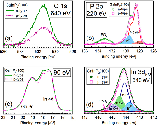
Figure 1. Surface-sensitive O 1s (a), P 2p (b), Ga 3d/In 4d (c) and In 3d5/2 (d) core level spectra measured at room temperature using indicated excitation energies on the etched/annealed n- and p-GaInP2(100) surfaces. Fitting components in P 2p spectra (b) are shown as guide for the eye. Fitting components in In 3d5/2 spectra are shown as filled or solid curves (p-type) and dot lines (n-type). The spectra of n-GaInP2(100) surface are shifted by 0.9 eV towards lower binding energies to align spectra for n- and p-GaInP2(100) surfaces in order to show differences in their shapes.
Download figure:
Standard image High-resolution imageAfter Shirley background subtraction, the P 2p core level spectra can be fitted with four components using Voigt functions with a spin-orbit splitting energy of 0.8 eV, a branching ratio of 2, and a Gaussian width of 0.65 eV, while the Lorentzian width is varied to obtain the best deconvolution [25] (figure 1(b)). In addition to the main P–Ga/In component with a binding energy of 129.4/128.5 eV for n-/p-GaInP2(100) surfaces, respectively, associated with the bulk P–Ga and P–In bonds, there are two components shifted to the higher binding energies by 1.0 and 4.4 eV, as well as a component shifted to the lower binding energy by 0.5 eV. The latter component can be considered as the surface component (Psurf); while the other chemically shifted components can be assigned to elemental phosphorous (P0) and to remnants of indium phosphate species (POx ) [24, 25] though the presence of surface phosphorous oxides cannot be excluded as well. Obviously, the relative intensities of the surface and elemental phosphorous components are similar in the spectra of both n- and p-GaInP2(100) surfaces (figure 1(b)). The coverage of elemental phosphorous component can be estimated as about 0.4 ML. On the other hand, the etched/annealed n-GaInP2(100) surface contains much more residual indium phosphates/phosphorous oxides (about 0.45 ML) than the p-GaInP2(100) surface (about 0.05 ML). It should be noted that the initial content of phosphates at the native-oxide-covered surfaces prior to etching was similar for both n- and p-GaInP2(100) surfaces. The larger amount of indium phosphates/oxides on the n-GaInP2(100) surface is visible also in the surface-sensitive In 4d spectrum (figure 1(c)). At the same time, the shape of the Ga 3d spectrum and thus the composition of residual gallium oxides is essentially independent of the conductivity type of the GaInP2(100) surface (figure 1(c)). It should be noted that in GaInX compounds, the exact unambiguous fitting of the Ga 3d and In 4d core levels due to proximity of their binding energies is a very complex problem since two different spin-orbital splitting energies and branching ratio values should be considered simultaneously [24, 25]. Therefore, to compare the composition of the residual indium surface oxides on the n- and p-GaInP2(100) surfaces, the In 3d core levels measured with the excitation energy of 540 eV were analyzed (figure 1(d)).
Obviously, the In 3d5/2 core level spectrum of n-GaInP2(100) surface is somewhat broader than the spectrum of the p-GaInP2(100) surface (figure 1(d)), indicating larger amount of indium oxides/phosphates, in agreement with O 1s, P 2p and In 4d (figures 1(a)–(c)) core level spectra. The In 3d5/2 core level spectra can be fitted with five different components (figure 1(d)). The In–P bulk components occur at the binding energies of about 445.0 and 444.1 eV for n- and p-GaInP2(100) surfaces, respectively. Besides, the deconvolutions of both spectra contain four other components, which shifted from the In–P bulk component by −0.35 eV (i.e. to lower binding energies), as well as by 0.35, 0.8, and 1.3 eV (i.e. to higher binding energies). These components can be assigned to metallic indium (In0), indium chlorides (In–Cl) formed in the course of etching with HCl solution, indium hydroxides (In–OH), and residual indium phosphates (InPOx ), respectively [24, 25]. It should be noted that the indium phosphate component (InPOx ) is hardly observed in the fitting of the In 3d5/2 spectrum of p-GaInP2(100) surface (its intensity is below 1% of the intensity of In–P bulk component), while in the spectrum of n-GaInP2(100) surface this component is much larger (figure 1(d)). This is in agreement with a larger phosphate component in the P 2p core level spectrum of the n-GaInP2(100) surface (figure 1(b)). The In–OH component is also somewhat larger at the n-GaInP2(100) surface than at the p-GaInP2(100) surface (figure 1(d)).
So, after etching of the native oxide layer from the GaInP2(100) surface with 1.25 M solution of HCl in 2-propanol the amount of residual oxides left on the n-GaInP2(100) surface is larger than on the p-GaInP2(100) surface.
In order to understand the effect of temperature on the surface Fermi level position at n- and p-GaInP2(100) surfaces, the photoemission spectra were also measured on the samples cooled down to the liquid-nitrogen temperature (77 K). The surface band bending of a semiconductor can be determined from the binding energy of the core level since the difference between the core level binding energy and the valence band edge is constant for each certain material [26]. In particular, the difference between the binding energy of the P–Ga/In bulk component of the P 2p core level spectrum (figure 1(a)) and the binding energy of the valence band onset of the GaInP2 can be estimated as 128.0 eV (figure 2). Taking this value into account, it can be concluded that the energy separation between the surface Fermi level and the valence band maximum on the etched p-GaInP2(100) surface decreases from 0.5 to 0.15 eV when the sample temperature is reduced from 300 to 77 K (figure 2). To obtain the band bending value, the energy separation between the Fermi level and valence band maximum in the bulk should be subtracted from these values. The value of this energy separation  can be evaluated from electroneutrality of the sample
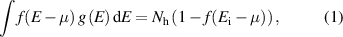
Figure 2. P 2p core-level spectra measured with an excitation energy of 220 eV, and spectra of the valence band edge measured with the excitation energy of 90 eV at room (300 K) and liquid-nitrogen (77 K) temperature on n- and p-GaInP2(100) surfaces. The kinetic energies of P 2p and valence-band-edge photoelectrons are nearly the same and correspond to an information depth of about 15 Å.
Download figure:
Standard image High-resolution imagewhere f(E) is the Fermi–Dirac distribution function,  is ionization energy of acceptor,
  is the density of states for holes in the bulk,
  is the effective density of states in the valence band, and Nh is the total number of free holes [27, 28] which is about 1 × 1017 cm−3 at 300 K. The integral should be taken over all energy values.
  value for Ga0.5In0.5P was estimated as the average of the values for GaP and InP [29]. For p-GaInP2, the separation can be evaluated as 0.124 eV at 300 K. The energy separation between the Fermi level and conductance band minimum for n-type of GaInP2 obtained in similar way is 48 meV at 300 K.
On the n-GaInP2(100) surface, the energy separation from the valence band maximum to the surface Fermi level increases by a similar value from 1.4 to 1.75 eV, which also corresponds to the reduction of the band bending with the decrease in temperature (figure 2). However, to determine the exact values of the band bending on n-GaInP2(100) surface at 300 and 77 K the temperature dependence [30] of the GaInP2(100) bandgap should be taken into account.
4. Discussion
Usually, the semiconductor surface band bending changes under any optical excitation. In the simplest case of the surface depletion layer caused by the occurrence of the occupied surface states, the non-equilibrium carriers generated in the semiconductor bulk on light absorption balance the charge localized at the surface states. This will cause the reduction in the surface band bending called as the surface photovoltage. This band flattening should occur at any temperature if the surface states are fully occupied by charge carriers in the dark. The temperature affects only the position of the chemical potential with respect to the surface state level. Since the chemical potential position is set by the semiconductor bulk parameters, the temperature change should affect the surface band bending both at equilibrium and under light irradiation; though under light irradiation the surface band bending will be somewhat smaller than at equilibrium due to surface photovoltage.
The observed reduction of the semiconductor surface band bending at low temperature (figure 2) is usually explained qualitatively by the effect of surface recombination [31]. At room temperature, the electron–hole pairs created in the surface region of the semiconductor by photoemission excitation recombine very fast due to the high surface recombination velocity and thus the thermodynamic equilibrium is not violated. At low temperatures, the surface recombination diminishes and the electron–hole pairs excited by x-ray radiation lead to a flattening of the semiconductor bands at the surface. However, the exact reasons for the reduction of the surface recombination velocity at low temperatures are unclear so far. Besides, as all methods for surface band bending determination include optical excitation, the question arises whether the surface band bending of the semiconductor is indeed reduced at low temperatures, or this is just an apparent flattening caused by optical excitation in the course of band bending measurement.
In the following, in the framework of general methods of charge carriers' statistics in semiconductors [27, 28] it will be shown that the flattening of the semiconductor bands at low temperatures can be observed even without external light excitation, i.e. in equilibrium. No additional assumptions are necessary, while the parameters of the surface states will be used as fitting parameters. The synchrotron excitation under conditions of a real experiment causes only a certain reduction of the surface potential, but has no essential influence on its temperature dependence.
The surface band bending is determined by the balance of charges localized in the surface states, in the bulk impurity levels, as well as by the free majority carriers in the conduction or valence bands in the n-type or p-type semiconductor, respectively. The temperature reduction results in the redistribution of charges. In particular, the number of majority carriers decreases due to incomplete ionization of impurity atoms, which causes a reduction of the number of charges in the surface states. Therefore, the surface potential value decreases as well.
The surface states trap charge carriers from the semiconductor bulk causing the bending of the semiconductor bands and formation of the space charge layer near the surface to fulfill the condition of overall charge neutrality.
The electrostatic potential  should obey the Poisson equation in which the z-axis is directed along the surface normal into the bulk of the semiconductor:

Here  is the charge density and
  is the static dielectric constant of the semiconductor. The equality of the potential to zero in the bulk of the semiconductor can be considered as boundary condition:
The second boundary condition is the equality of the electrostatic field at the surface (at z = 0) to the field induced by the surface states, which is defined by the surface charge density.
In the non-degenerated semiconductor in which the charge carriers obey Boltzmann statistics the charge density is

Here q is the electronic charge, ni is the density of intrinsic carriers,  is the parameter characterizing deviation of the carrier's concentration from the intrinsic concentration, n0 is the equilibrium bulk electron concentration in the case of non-degeneracy,
  is the dimensionless electrostatic potential. In the parenthesis of equation (3) there are charges of free holes, free electrons, as well as charged donors and acceptors.
The first integral of the equation (2) with the charge density (3) is the electric field, which with the account for zero electric field in the bulk can be written as
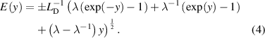
Here the Debye shielding length is introduced as
The sign in the equation (4) is determined by the direction of the band bending. Plus or minus is used in the case of upward or downward band bending, respectively.
Both n- and p-GaInP2(100) semiconductors used in the present study have a depleted near-surface region. In the case of depleted n-type semiconductor, the equation (4) can be simplified as follows:

For the p-type semiconductor the corresponding equation takes the form

However, these equations can be considered as equivalent because in the case of depleted space charge layer y < 0 for n-type semiconductor and y > 0 for p-type semiconductor.
The band diagrams of the depletion layer of n- and p-type semiconductors are shown in figure 3. To obtain the surface band bending value, the chemical potential should be subtracted from the experimentally obtained binding energy of the valence band maximum. For correct calculations, the temperature dependence of the semiconductor band gap should be taken into account.
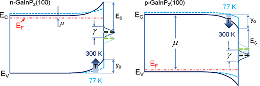
Figure 3. Energy band diagram of the n-type and p-GaInP2(100) at 77 and 300 K. Here y0 is the surface band bending at room temperature; µ is the Fermi level position relative to the conduction band minimum in the bulk; ES is the energy position of the surface states relative to the conduction band minimum; γ is a broadening of the surface state level.
Download figure:
Standard image High-resolution imageTo fulfill the charge neutrality condition, the total charge at the surface Qs (negative if the surface states are occupied by electrons) should be equal to the total positive charge in the near-surface space charge layer. According to Gauss electrostatic law, this charge is proportional to the electric field at the surface
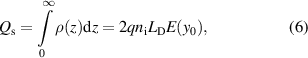
where y0 is the potential at the surface (figure 3).
As the surface charge includes the charges in the filled surface states by electrons (or holes) with the energy difference Es measured from the conduction band minimum and surface density Ns (this is the adjustment parameter that is supposed to be known, for example, from other experimental observation), the relationship between the parameters of the surface states and the surface band bending can be obtained.
To verify the proposed model, the surface energy levels in gallium arsenide were calculated, for which a large number of experimental data is available. The band bending values obtained by synchrotron-radiation photoelectron spectroscopy for n-GaAs(100) with the electron concentration of 2 × 1018 cm–3 were 0.74 eV at 300 К and 0.43 eV at 77 К [32]. In calculations, it was assumed that the donor ionization energy is 4 meV [29].
Let us suppose that the surface states represent a single level located in the bandgap. Then for n-GaAs it follows from equation (6) that the surface state density should be of the order of 1014–1015 cm–2. Such values seem to be too large as it is of the order of the total number of surface atoms, and thus it was assumed in the following calculations that the surface state levels are broadened as
Here γ is a broadening parameter of the surface state level. In the limiting case of  the equation (7) transforms to the case of the single level.
Therefore, taking into account the expression (6), one obtains the equation
If the experimentally available values of the surface band bending y0 at different temperatures and the other parameters are known, the density of surface states can be obtain from the solution of the equation (8). In this case, the parameter γ is selected so that the values of the surface potential  and
and  coincide with the experimental results. In this regard, the equation (8) was solved twice for the two temperatures 300 K and 77 K. From the obtained, which is an indicating factor for the reduction of the surface band bending when the temperature is reduced from 300 K to 77 K.
So, for n-GaAs with  = 1.7 [32], one can obtain NS0 = 5 × 1011 cm–2; ES = 0.62 eV; γ = 1 eV. This corresponds to a smooth distribution of the surface states over the whole band gap with the maximum near 0.62 eV from the minimum of the conduction band, which is in a good agreement with available experimental data [33].
The calculated values of the surface level energy ES in n-GaInP2 and p-GaInP2 as a function of  are shown in figure 4 for different values of the surface state density. These dependencies can be used for the estimation of the surface state density and spectrum when the value of
  can be obtained from experimental data.
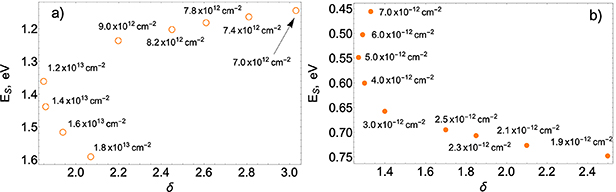
Figure 4. Dependence of the surface state energy on  for p-GaInP2 (a) and n-GaInP2 (b). The numbers indicate the density of surface states. The energy of the surface state level is measured from the bottom of the conduction band. The difference between the values of
  is due to the different ionization energy of impurities in n- and p-type semiconductors.
Download figure:
Standard image High-resolution imageFigure 4 shows that two possible solutions occur if the energy of the level approaches the conduction band minimum for n-GaInP2 or the valence band maximum for p-GaInP2. The closer the energy of the level to the corresponding band edge, the higher is the density of surface states. This multiplicity/ambiguity is due to the stronger influence of the position of the electrochemical potential on the occupation of the surface states when the surface levels are close to the band edges. If these levels occur in the depth of the band gap, the occupation of the surface states will be close to unity. Therefore two different solutions of the equation (8) corresponding to different energy and density of surface states can exist for one value of  . In this case, for a reasonable estimation of the surface state energy, the additional data on the surface state density is necessary.
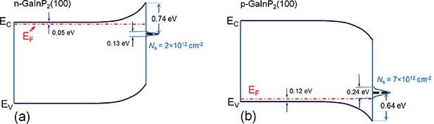
For n-GaInP2(100) with the doping density of p ∼ 1017 cm–3 the band bending can be calculated as 350 and 140 meV at 300 and 77 K, respectively ( ). Solving the equation (8), one can obtain that the level of the surface states occurs at the energy of 0.74 eV below the conduction band minimum, the broadening of the surface states level is about 130 meV, and the surface states density is of about 2 × 1012 cm–2 (figure 5(a)), which is in a good agreement with the data obtained previously for the HCl-etched n-GaInP2(100) surface [16]. For p-GaInP2(100) (band bending is 370 and 130 meV at 300 and 77 K, respectively
  ) similar calculations give the energy of the surface states of 0.64 eV above the valence band maximum, the broadening of the surface state level is 240 meV, while the surface states density is of the order of 7 × 1012 cm–2 (figure 5(b)).
Figure 5. Calculated energy band diagrams of the n-type (a) and p-GaInP2(100) (b) with the doping density of ∼1017 cm–3 at 300 K.
Download figure:
Standard image High-resolution image
Thus, the agreement of the experimental data with the values obtained from the proposed model testifies that the band bending at the n- and p-GaInP2(100) surface is reduced at low temperature. On the other hand, surface photovoltage caused by synchrotron irradiation will have some contribution to the band flattening. This effect will strongly depend on the level of illumination, therefore light intensity variations may be used for discriminating the effects from each other. Further experiments intended for elimination/reduction of the effects of optical excitation are necessary to estimate the contribution of the surface photovoltage to the reduction of the surface band bending.
5. Conclusions
The variation of the band bending in n- and p-GaInP2(100) surfaces as a function of temperature has been determined experimentally using SXPS. It is found that this effect can be observed even in the equilibrium state, i.e. without any external excitations that cause formation of the non-equilibrium carriers and their subsequent recombination. The observed changes can be explained in the framework of semiconductor surface electrostatics. This effect is related to charge redistribution between surface and bulk states in the semiconductor under temperature variation. The proposed model enables quantitative characterization of the surface state spectrum based on the experimentally determined values of the surface potential at different temperatures.
Acknowledgements
Authors acknowledge support from the Russian Foundation for Basic Research (Grant No. 20-03-00523).