

Abstract
In this paper, we experimentally examined the threshold voltage (VT) variability and the corner effects in gate-all-around p-type poly-Si junctionless (JL) nanowire (NW) and nanosheet (NS) transistors as a function of various effective channel width. The fabricated devices showed small VT variability characteristics even in poly-Si JL NW channel structure thanks to the improved quality of poly-Si channel by fluorine (F) passivation and reduced channel concentration by boron (B) segregation. In addition, it was found by examining the corner effects that the fabricated devices exhibit accumulation-mode like behaviors. The origins of these phenomena are discussed.
Export citation and abstract BibTeX RIS
1. Introduction
Polycrystalline silicon (poly-Si) based transistors have been spotlighted as the key building elements for 3D multi-stacking technology owing to the low-cost, easy integration, and simple fabrication methods. 1–3) Basically, the poly-Si channel is composed of grains separated by grain boundaries (GBs) with high density of trapping states, which solely determines the electrical performances of poly-Si transistors. Hence, it should be required to enlarge the grain size or reduce the trapping states at GBs in order to achieve high-performance poly-Si transistors. 4,5)
Meanwhile, the concept of junctionless (JL) transistors (or gated resistors) without source/drain (S/D) junctions has attracted much interest due to the simple fabrication, elimination of impurity diffusion, and volume conduction. For the JL transistors, the on-current is mainly determined by channel concentration, so that the doping concentration of the channel should be as high as possible to ensure high on-current and low series resistance in the turn-on state. In addition, the JL channel must be thin enough for full depletion in the turn-off state, which significantly affects subthreshold characteristics. 6–8)
Gate-all-around (GAA) nanowire (NW) architecture can be well matched with poly-Si JL transistors for a reduced total number of GBs and improved subthreshold characteristics, as well as enhanced gate controllability. 9–11) Therefore, high-performance GAA poly-Si JL NW transistors can be obtained by suppressing the GB defects and adopting a small-size NW channel.
However, one of the most critical issues in GAA poly-Si JL NW transistors is the difficulty of achieving sufficiently small characteristics variability among adjacent transistors for the application of future advanced electronics. There are three main factors to affect the variability characteristics of poly-Si JL NW transistors. One is the GB in the poly-Si channel, the second is the feature of JL transistors, and the third is related to the GAA NW architecture.
The presence of high-density trapping states at GBs in poly-Si channel degrades not only carrier transports but also device-to-device variability characteristics, which produces severe delay and power consumption. These harmful GB defects are randomly positioned in the poly-Si channel, whose numbers, orientations, shapes, and qualities are different among transistors. In addition, these high variability characteristics from the GB defects become more serious when the transistors are scaled down to nanometer size, i.e. NW transistor due to increased randomness of GBs placements. 4,12,13)
For the JL transistor, it has a high doping concentration with uniform and homogeneous across the source, channel, and drain regions. For the reasonable high on-current, the doping concentration of the JL channel should be as high as possible (≥1 × 1019 cm−3). However, this high channel concentration of JL transistor produces severe device-to-device variability issues such as threshold voltage (VT) fluctuation induced by the random dopant fluctuation (RDF). In addition, the VT fluctuation by RDF rapidly increases as the transistor is scaled down. 14–16) As a result, the JL transistors basically exhibit significantly high variability characteristics compared with conventional inversion mode (IM) transistors with a nearly intrinsic channel.
In general, NW is formed by the top-down approach method using lithography techniques. However, this method leads to a large variation of NW width as well as non-uniformity of NW size and asymmetric shapes (circle, rectangular, rhombus, and triangle). 17–20) Hence, the line edge roughness arises from the non-uniformity and asymmetric shapes of the NW channel, which also enhances the corner effect in which the electric field is concentrated at the corner in the non-uniform NW shapes. 21) This corner effect produces additional current at each corner of NW by the high electric field and severe VT fluctuation between adjacent transistors due to the large variations of NW width.
Based on these backgrounds, it can be seen that the GAA poly-Si JL NW transistor basically has poor variability characteristics. However, comprehensive studies on the variability issues of the GAA poly-Si JL NW transistors have not been reported yet.
In our previous work, 22) we implemented the high-performance GAA poly-Si JL NW transistors with relatively high carrier mobility (25.5 cm2 V−1·s−1), ideal SS (60.08 mV dec.−1), small SS variations, and high thermal stability by improved quality of poly-Si channel by F passivation and B segregation. The width (W) and height (H) of the GAA NW channel were 9.6 nm and 6.7 nm, respectively, and the total number of GB defects inside the poly-Si NW channel was sufficiently reduced.
In this study, therefore, the variability characteristics of VT and ID as a function of effective channel width in the p-type GAA poly-Si JL NW and nanosheet (NS) transistors and their corner effects are highlighted. This paper is an extended version of Ref. 23, in which more measured data and discussions are included.
2. Experimental methods
2.1. Device fabrication process flows
The fabrication process flows basically follow Ref. 22. Figure 1(a) shows key fabrication process steps, and Figs. 1(b) and 1(c) show 3D schematic structures and cross-section of fabricated p-type GAA JL poly-Si NW transistors. A 120 nm thick undoped amorphous Si (a-Si) was deposited on a 200 nm thick BOX layer by low-pressure chemical vapor deposition (LPCVD) at 560 °C in 33 Pa, and solid-phase crystallization was conducted at 1100 °C for 24 h. BF2 + ions were implanted with an ion energy of 35 keV and a dose of 3 × 1014 cm−2 to form a p+ poly-Si channel, because we already demonstrated that the BF2 + implanted poly-Si JL transistor exhibited better SS and higher mobility than that of B+ implanted one owing to the F passivation effect. 24) Then, the active channel region was locally thinned down to 20 nm by thermal oxidation at 1100 °C, by which the B concentration of thinned active region was reduced due to the segregation of B ions, resulting in P+/P/P+ structure with low channel concentration in a self-align manner. The estimated B concentration in the thin P channel is around 1 × 1018 cm−3 by secondary ion mass spectroscopy depth profiles (data not shown). Then, NW/NS channels were defined by the electron beam lithography and reactive ion etching, followed by HF wet-etching by which the BOX layer under NW/NS channels was etched to form suspending NW/NS above the BOX layer. Next, a 7 nm thick SiO2 layer was thermally grown as the gate oxide, and in-situ phosphorus-doped poly-Si using SiH4 and PH3 with 33 Pa by LPCVD at 560 °C was formed as a gate electrode. Then, a 300 nm thick SiO2 was deposited for passivation and H2 annealing was carried out to eliminate the defects at 400 °C for 30 min. Finally, Al metal contacts were formed.

Fig. 1. (Color online) (a) Key fabrication process flows, (b) 3D schematic, and (c) cross-section of fabricated p-type GAA JL poly-Si NW transistors.
Download figure:
Standard image High-resolution imageThe NW/NS length (L) and height (H) are 250 nm and 7 nm, respectively. The NW width (W) ranges from 10 to 25 nm and NS width from 55 to 130 nm. The effective width (Weff) is a perimeter of NW and NS, ranging from 34 to 274 nm.
2.2. Substrate bias
Since the NW/NS device structure has a long gate length of 30 μm (short channel effects are negligible), the NW/NS channel is connected to large S/D and extension regions. These extension regions operate as the parasitic transistors, so that the electrical performances would be underestimated. Since the structure of parasitic transistors is planar, VT of the parasitic transistor is shifted by the body effect, while VT in the NW/NS transistor is never changed due to the GAA structure. To eliminate the parasitic effects, high negative substrate bias (Vsub = −25 V) should be applied to obtain actual NW/NS characteristics. Therefore, the variability characteristics and corner effects were evaluated at a condition of Vsub of −25 V in this paper. 22)
3. Results and discussion
Figure 2 shows the measured ID–VG characteristics of fabricated NW/NS transistors with W ranging from 10 to 130 nm (Weff ranging from 34 to 274 nm) at VD = −0.05 V with L of 250 nm. The number of transistors in each size is 40 – 50. A substrate bias of −25 V was applied to eliminate the parasitic effects. 22,25) It is clearly seen that the variability characteristics among neighboring transistors become worse as Weff decreases, which is attributed to the increased randomness of GBs placement and RDF. We can clearly observe that the distributions of ID–VG characteristics become tighter as Weff increases.

Fig. 2. (Color online) ID–VG characteristics of fabricated NW/NS transistors with W ranging from 10 to 130 nm (Weff ranging from 34 to 274 nm) at VD = −0.05 V in L of 250 nm. In each transistor size, around 40 – 50 transistors were evaluated.
Download figure:
Standard image High-resolution imageFigure 3(a) shows the statistic distributions of VT as a function of various Weff with L of 250 nm. VT is extracted at ID = 108 × Weff/L. It is more clearly observed that the VT variability significantly depends on Weff, showing that the largest NS (Weff = 274 nm) has the smallest VT distributions. In order to more clearly figure it out, the average VT values and standard deviations of VT (σVT) are evaluated as shown in Fig. 3(b). One can see that σVT gradually decreases as Weff increases, which is consistent with the results of previous reports showing that the variability characteristics are reduced as the W increases. 17,20)

Fig. 3. (Color online) (a) Statistic distributions of VT, and (b) extracted average VT values and standard deviations (σVT) as a function of various Weff in L of 250 nm.
Download figure:
Standard image High-resolution imageFigure 4 displays the Pelgrom plot of fabricated NW and NS devices with Weff from 34 to 274 nm at L of 250 nm. We compare with the previous reported poly-Si NW IM transistors, 4,26) poly-Si NW JL transistors, 27) and bulk Si MOSFET (LG = 60 nm), 28) whose key parameters affecting σVT are summarized in Table I. The σVT basically follows:

where the Tox and Nch are gate oxide thickness and channel concentration, respectively. Weff is used for W. To eliminate the effect of Tox on the variability characteristics, σVT is divided by Tox (y-axis: σVT/Tox) for more reasonable comparisons. The clear linearity of the σVT/Tox as a function of 1/(LWeff)1/2 is observed in our result. First, the slope of the Pelgrom plot is compared with that of poly-Si JL transistors. It is found that the present device shows a much smaller slope than that of the poly-Si JL transistors in Ref. 27. This is due to a better quality of poly-Si by F passivation effect and a lower channel concentration by the B segregation. 22–25) The small VT variability is a great advantage of our JL devices. The larger slope of this work compared with IM poly-Si transistors in Ref. 26 can be explained by high channel concentration in the JL structure. In general, the JL transistors exhibits considerably high variability characteristics compared with IM transistors due to high channel concentration by the RDF. However, the result of the present devices shows a comparable slope with poly-Si IM 4) and bulk transistors 28) thanks to the lower channel concentration by the B segregation.
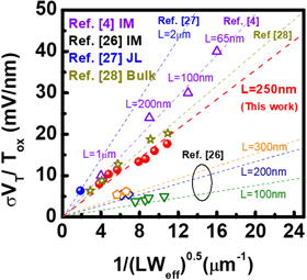
Fig. 4. (Color online) Pelgrom plot of σVT/Tox. Previous reported data are also shown, Refs. 4, 26–28. Closed and open symbols represent the data of JL and IM transistors, respectively.
Download figure:
Standard image High-resolution imageTable I. Key parameters affecting σVT. Published poly-Si based NW IM, JL transistors, and bulk MOSFET are compared.
| This work | Ref. 4 | Ref. 26 | Ref. 27 | Ref. 28 | |
|---|---|---|---|---|---|
| Device type | NW_JL | NW_IM | NW_IM | NW_JL | Bulk |
| Crystallinity | Poly crystal | Poly crystal | Poly crystal | Poly crystal | Single crystal |
| Weff [μm] | 0.034–0.274 | 0.024 | 0.05–0.08 | 0.144 | 0.14–2 |
| L [μm] | 0.25 | 0.065–1 | 0.1–0.3 | 2 | 0.06 |
| Tox [nm] | 7 | 2 | 8 | 13 | 2 |
| Nch [cm−3] | ∼1 × 10¹⁸ | ∼1 × 10¹⁵ | ∼1 × 10¹⁵ | ∼5 × 10¹⁸ | ∼1 × 10¹⁸ |
The dependences of ID variability characteristic on Weff are discussed based on the measured ID–VG curves. Figure 5(a) shows the statistic distributions of ID as a function of various Weff with L of 250 nm, where ID is not normalized to Weff and extracted at the gate overdrive voltage (Vov = VG − VT) of −2 V. It can be observed that ID does not linearly increase as Weff increases. In addition, ID/Weff decreases despite Weff increases as shown in Fig. 5(b).
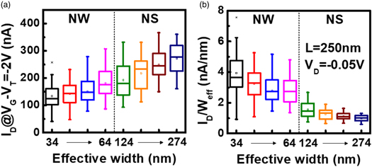
Fig. 5. (Color online) Statistic distributions of ID as a function of Weff in L of 250 and 350 nm. (a) ID is not normalized. (b) ID is normalized to Weff.
Download figure:
Standard image High-resolution imageThe origin of this non-linear ID characteristic can be considered as the corner effects. As mentioned before, the corner effects of NW transistors usually produce severe VT fluctuation due to concentrated high electric fields at each corner of the non-rounded NW channel with large variations of NW width among adjacent transistors. In addition to VT fluctuation, the additional corner current (ID_corner) can be introduced by concentrated high electric fields, which can produce non-linearity ID characteristics. 29–31) Even though it is well known that the JL transistors have a small corner effect due to unique volume conduction, one of the possible reasons for this ID non-linearity is the additional ID_corner by the high electric field at the corner of NW even in the JL transistor.
In order to investigate the corner effects, the total ID (ID_total) as a function of WNW × HNW at different Vov of −3 V (far from VT), −1 V, −0.1 V (near the VT) is plotted in Fig. 6. ID_total is the sum of volume current (ID_vol), flat surface current, and corner current (ID_total = ID_vol +ID_surface + ID_corner). When the WNW × HNW approaches to zero, the ID_vol and ID_surface become zero, so that ID_total roughly corresponds to ID_corner (y intercept). Near the flat band condition (Vov = −0.1 V), the ID_total approaches to almost zero as WNW × HNW approaches to zero indicating the corner effect is negligible, while high ID remains at Vov = −3 V as WNW × HNW approaches to zero. This is because holes are accumulated at the corner due to the high electric field at Vov = −3 V (corner effect).

Fig. 6. (Color online) Extracted average ID_total as a function of WNW × HNW at different Vov of (a) −3 V (far from VT), (b) −1 V, and (c) −0.1 V (close to VT). The inset shows a schematic of NW cross-section showing the carrier density distribution (cartoon).
Download figure:
Standard image High-resolution imageFollowing the component separation method, 31) the ratio of the ID_corner component can be derived. Figure 7 shows the ratio of ID_corner (fixed y-axis intercept) of ID_total with different four Weff as a function of various Vov. Apparently, the narrower NW has a larger fraction of ID_corner, and it drastically decreases as VG approaches VT due to the volume conduction of JL transistors. It can be speculated here that the voltage difference between VT and VFB of the present devices remarkably small. This behavior is different from conventional JL transistor with high channel concentration. In the present devices, the channel has low concentration by B segregation, so that VT is close to VFB, resulting in accumulation-mode (AM) like behaviors 32–34) rather than normal JL operation as shown in Fig. 8. On the other hand, the VT variability is not affected by the corner effect unlike the IM devices because the corner effect is not dominant around VT. This is also a merit of the present devices because the higher on-current can be obtained even in a narrow NW structure while the VT variability is suppressed.

Fig. 7. (Color online) Ratio of ID_corner (fixed y-axis intercept) of ID_total with different four Weff as a function of VOV.
Download figure:
Standard image High-resolution image
Fig. 8. (Color online) Schematic ID–VG characteristics of conventional p-type JL transistors and the device in this study. The lower channel concentration of the devices in this study results in AM like behavior (VFB is close to VT).
Download figure:
Standard image High-resolution image
4. Conclusions
In summary, comprehensive studies on the variability characteristics and corner effects of GAA p-type poly-Si JL NW/NS transistor were experimentally examined. We clearly observed that variability characteristics become worse as Weff decreases, which is attributed to the increased randomness of GBs placement and RDF. It was found from the Pelgrom plot that the present poly-Si JL transistors show smaller σVT than previous reported JL transistors and comparable with poly-Si IM and bulk transistors. In addition, it was found that the reduced channel concentration by B segregation makes the JL transistor to operate as AM like behaviors. As a result, relatively small VT variability characteristics, as well as high on-current, were achieved in the GAA poly-Si JL NW transistors in this study, which is likely to be useful for future low power 3D applications.