

Abstract
Transition metal dichalcogenides (TMDs) attract research interest owing to their unique physical and chemical properties. Among the family of TMDs, tungsten disulfide (WS2) has a unique band structure due to its semiconductor characteristics; namely, its broadband spectral response characteristics, ultra-fast bleach recovery time and excellent saturable light absorption. This article is a review of the current application of WS2 in catalysts, lasers, batteries, photodetectors and lubricants. The review begins with a brief overview of the structure, properties and growth of WS2 and describes the existing preparation methods for this material. Finally, methods for improving the performance of WS2 in its current applications are presented. This review is limited to the most recent reports on this topic.
Export citation and abstract BibTeX RIS
1. Introduction
Linus Pauling first determined the structure of transition metal dichalcogenides (TMDs) in 1923 [1] and more than 60 TMDs have been discovered since 1960 [2]. Stable graphene was isolated from graphite in 2004 [3], which opened a new path for the application of ultra-thin films of TMDs [4]. There are 44 TMD compounds that can form stable two-dimensional (2D) structures, which have the composition MX2, where M is a transition metal and X is S, Se or Te [5]. These compounds exhibit the physical properties of metals, semiconductors, superconductors and insulators [4]. Among these TMDs, WS2 has a unique band structure that results from its semiconductor-related properties, such as broadband spectral response characteristics, ultrafast bleach recovery and excellent saturable light absorption [6]. Owing to the physical and chemical properties of WS2, it is widely applied in many fields. This article reviews the properties, preparation and applications of WS2. In section 2, we briefly discuss the structure, properties and growth of WS2, and, in section 3, its current preparation methods are discussed. The applications of WS2 in catalysis, lasers, batteries, lubricants and other fields are discussed in section 4. Finally, the improved performance of WS2 in various fields is discussed.
2. Introduction to WS2
2.1. Structure of WS2
The structure of WS2 comprises stacked triple layers formed by a transition metal layer (W atom) sandwiched between two S atom layers, each of which has a hexagonal lattice structure. In the three-layer stack, W atoms and S atoms are bonded by strong ionic-covalent bonds. The structure formed by these three layers is held together by weak van der Waals interactions, which allow mechanical peeling of WS2 layers. In the bulk phase, polymorphisms are unique features of TMDs. The atomic structure of WS2 depends on the filling of the d-orbitals in the transition metal [7]. There are three possible stacking structures of WS2 (figure 1), namely, 1T, 2H and 3R. The 1T structure is formed by tetragonal symmetry and octahedral coordination. The d-orbitals of transition metals are divided into two energy levels: dxy, yz, zx and dx 2 −y 2 ,z 2. The 2H structure is formed by hexagonal close packing and coordination of triangular prisms, and 3R is a rhombic symmetrical structure [8]. In the 2H and 3R phases, the d-orbitals of transition metals are divided into three energy levels: dz 2, dx 2 −y 2 , xy and dxy, yz . For a single-layer WS2 film, the 2H structure is the most stable and the most common structure. In addition to the more common 1T, 2H and 3R stacked structures mentioned in this article, WS2 also has a 1T' structure, which has also attracted widespread attention owing to its excellent topological insulation characteristics [9].

Figure 1. Unit cells of WS2 polymorphs [8]. [Copyright © 2014], reprinted by permission of the publisher (Taylor & Francis Ltd, http://www.tandfonline.com).
Download figure:
Standard image High-resolution imageTo change the atomic structure of WS2, the lithium-ion intercalation method and the nonintercalation phase transformation method are often used. Lithium-ion intercalation is a reversible process. When an excess charge is added, the 2H phase transition becomes unstable and changes to the 1T phase; however, when the lithium ion is removed from WS2, the excess charge is removed. Subsequently, the WS2 in the 1T phase is recovered to the most stable 2H phase [10]. The intercalation-free phase transformation method includes stimulation through infrared laser [11] and electron beam irradiation [12]. The reactions are irreversible. These reactions produce irreversible chalcogenide vacancies, which are the driving forces for the transition from 2H to 1T. However, this method is destructive and cannot reverse the phase transition from 2H to 1T. These phase transitions can change the properties of WS2 to between those of a semiconductor and a metal [13].
2.2. Properties of WS2
Owing to the influence of quantum confinement and interlayer interactions, indirect-to-direct bandgap transitions will occur when the thickness of WS2 is reduced to a single layer [14]. In general, with the change in the WS2 thickness, the direct bandgap at the K point is constant. This is because the corresponding valence and conduction band states at K are only related to the transition metal state and are not affected by the interlayer interactions. However, when the thickness of WS2 changes from two layers to one layer, the indirect bandgap from Γ to K is larger than the direct bandgap. This occurs because the valence band state at Γ is related to the  orbital of the metal and the PZ
orbit of the sulfur group element. For single-layer WS2, there is no Coulomb repulsion between the PZ
orbitals of chalcogenide elements in the adjacent layers, resulting in the stability of the valence band state of Γ, which causes indirect-to-direct gap transitions [15].
orbital of the metal and the PZ
orbit of the sulfur group element. For single-layer WS2, there is no Coulomb repulsion between the PZ
orbitals of chalcogenide elements in the adjacent layers, resulting in the stability of the valence band state of Γ, which causes indirect-to-direct gap transitions [15].
2.3. Growth of WS2
WS2 can grow in horizontal and vertical directions. In the horizontal growth process, the WS2 layer grows along the plane direction and the film is parallel to the growth substrate [16]. In the vertical growth process, the WS2 layer grows vertically on the growth substrate, exposing the edge position of the film [17, 18]. These two different morphologies lead to different material properties and have different applications. The horizontal growth of WS2 is mainly used in optoelectronic technology owing to its indirect-to-direct bandgap transition and large on/off ratio as a transistor. Because of the chemically reactive edge position of WS2 grown vertically, several electrochemical studies have been conducted [19]. The main reason for the two types of morphologies is the deposition thickness of the precursor. With the decrease in the precursor layer thickness, the WS2 thin films transition from vertical growth to horizontal growth [20].
3. Preparation methods
At present, there are a variety of synthesis methods for producing WS2. These methods are categorized into physical, chemical and stripping methods.
3.1. Physical methods
Physical methods include pulsed magnetron sputtering and pulsed laser deposition (PLD). The magnetron sputtering growth method requires the use of charged particles to bombard the surface of the target under vacuum conditions to cause the target to sputter. In this approach, the neutral target atoms or molecules are deposited on a substrate to form a thin film. Usually, an inert gas is glow discharged in a low-pressure environment to generate incident ions. For WS2 deposition, a cathode target made of WS2 is sputtered under a high negative cathode voltage of 1–3 kV DC or a 13.56 MHz radiofrequency voltage. In addition, 0.1–10 Pa argon gas is passed into the vacuum chamber to generate glow discharge. Under the action of an electric field, Ar ions are accelerated toward the WS2 target and bombard the target surface with high energy, which removes small particles of the target material that deposit on the substrate to form a WS2 film [21]. To improve the adhesion of WS2 coatings, Rodrigues et al [22] deposited a Cr intermediate layer with a thickness of approximately 400 nm on a Si substrate and then deposited a WS2–CF coating (as shown in figure 2(a)). The important advantages of this method are the simple equipment, the low operating temperature of the substrate, large coating area and the ability to produce dense and well-adhered films [21].

Figure 2. Schematics of the deposition chambers for (a) WS2–CF coating prepared by magnetron sputtering. Reprinted from [22], Copyright (2018), with permission from Elsevier. (b) WS2 films prepared using PLD [23]. Reprinted from [24], Copyright (2018), with permission from Elsevier.
Download figure:
Standard image High-resolution imageIn contrast to magnetron sputtering, the equipment used for PLD is complex and its operating principle is relatively complicated. When a high-energy pulsed laser impacts the solid WS2 target, a laser pulse with a sufficiently high energy flux and short pulse width will be generated and the target is exposed to this pulse. The incident laser energy is absorbed by the target, resulting in a rapid temperature increase that causes some of the target to evaporate and form a localized high-temperature and high-density plasma. In accordance with the law of gas dynamics, the emitted plasma plume preferentially moves toward the substrate, thus forming a WS2 film [24]. In 2018, Tian et al [23] used PLD technology to grow controllable layers of WS2 thin films on sapphire substrates. They found that the thickness of the 2D WS2 films could be accurately controlled by controlling the number of incident pulses (monolayer and multilayer films were successfully prepared). Figure 2(b) shows a schematic of a deposition chamber for the growth of WS2 films using PLD. The most significant advantage of this method is that the thickness of the film can be controlled. The film is uniform and of good quality, but it has the disadvantages of high cost and complex operation.
3.2. Chemical methods
Two common methods for preparing WS2 films by chemical means are chemical vapor deposition (CVD) and growing single-crystal WS2 from an aqueous solution by the hydrothermal method under high-temperature and high-pressure conditions. CVD is the most common method used to prepare WS2.
The CVD method involves a reaction process in which a gaseous precursor undergoes a chemical reaction on a solid surface to generate a solid deposit. The preparation of WS2 by CVD can be achieved using either a one- or a two-step method. The one-step method involves the direct heating of sulfur and tungsten sources in a CVD furnace, followed by control of the carrier gas flow and then deposition of the WS2 film on the target substrate (as shown in figure 3(a)) [25]. A common tungsten source used is WO3, where the reaction 2WO3 + 7 S → WS2 + 3 SO2 occurs [26]. The most commonly used substrates are silicon, copper and quartz glass. The two-step method involves the deposition of a tungsten or tungsten compound film on the target substrate, which is then vulcanized in a CVD furnace to synthesize the WS2 film [27]. Usually, the deposition is carried out on the substrate by electron-beam evaporation or magnetron sputtering. For example, Carlo et al [28] prepared W films by magnetron sputtering and then sulfurized them. Their experimental results showed that the number of layers can be highly controlled by controlling the initial deposition thickness of W films, and WS2 thin films can be prepared over a large area using this method. CVD can accurately control the thickness and size of WS2 films by controlling the changes in temperature and carrier gas flow. High-quality WS2 films can be synthesized using CVD, with good optical and electrical properties. Moreover, the two-step method can also enable the preparation of large-scale films, thus overcoming the drawback of the one-step method. However, this method still has disadvantages such as the need for a high substrate temperature and relatively expensive equipment.
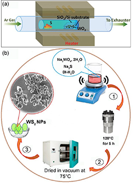
Figure 3. Schematic of the processes for producing WS2 thin films by (a) one-step CVD [25] John Wiley & Sons. [Copyright © 2014 WILEY-VCH Verlag GmbH & Co. KGaA, Weinheim]. and (b) hydrothermal method. Reprinted from [29], Copyright (2019), with permission from Elsevier.
Download figure:
Standard image High-resolution imageThe hydrothermal method is a typical wet chemical synthesis method. For preparing WS2 particles, the following representative process can be used [29]. First, 10 mmol of Na2WO4 2 H2O and 10 mmol of Na2S are dissolved in 50 ml of deionized water and continuously stirred for 30 min to form a clear solution. The solution is then transferred to a hydrothermal reactor at 220 °C for 5 h. The recovered solution is then centrifuged and rinsed with ethanol. Finally, WS2 particles are collected after vacuum drying at 75 °C (figure 3(b)). This method has been widely used in the preparation of 2D nanomaterials, especially WS2 particles. The advantages of the hydrothermal method are high purity, the crystallinity of the formed particles and facile control of the operating parameters [30]. However, the thickness of the films cannot be controlled when used in devices, and the reaction process is not visible.
3.3. Stripping methods
Bulk WS2 can be stripped by physical and chemical methods, which are classified into mechanical exfoliation, liquid exfoliation and lithium-ion intercalation methods. In recent years, to obtain large-area and high-quality single-layer WS2 films, researchers have tried to grow single-layer WS2 films on single-crystal substrates and then peel them off through atomic or molecular intercalation.
The mechanical stripping method is a simple physical method used to produce WS2 thin films. First, transparent adhesive tape is applied to the WS2 bulk laminated sheet to be stripped. The bulk material is then repeatedly peeled using the tape to thin the laminated sheet. Finally, the thin WS2 film is transferred from the tape to the target substrate (e.g. SiO2/Si), and the tape is slowly peeled off after a rest period to ensure that the WS2 film has adhered well to the target substrate (as shown in figure 4(a)) [31]. The prepared single-layer TMD materials have few defects and are highly crystalline, resulting in good photoelectric properties, such as high luminous efficiency and high carrier mobility. However, it is difficult to peel off a large-area film [32], which limits their practical applications, and the repetition rate is low.

Figure 4. Schematics showing WS2 film preparation by (a) mechanical stripping, Reprinted by permission from Springer Nature Customer Service Centre GmbH: [Springer Nature] [31], (2019). (b) liquid-phase stripping [33] Reproduced from [35]. CC BY 4.0. and (c) lithium-ion intercalation [34] (DMF = N-dimethylformamide). Reproduced from [36] with permission of The Royal Society of Chemistry.
Download figure:
Standard image High-resolution imageThe liquid-phase stripping method is based on the use of ultrasonic waves to generate cavitation bubbles or a shear force to separate the layered materials from each other. Then, the material is dispersed in a solvent to obtain 2D single-layer and few-layer materials [35]. The choice of solvent is the most critical factor in the liquid-phase stripping method. The surface tension of WS2 is estimated to be 40 mJ m−2 [36], so a suitable solvent must be selected to successfully peel the WS2 material. The most commonly used solvents are propanol, ethanol and water. To shorten the ultrasonic treatment time and improve the stability of the suspension, Adilbekova et al [33] used ammonia as the solvent for liquid-phase stripping. Figure 4(b) shows a schematic describing the preparation of WS2 films by the liquid-phase stripping method. This method can be used to prepare WS2 in large quantities, but the thickness of the WS2 film produced using this method is not uniform and the purity of the film is low.
The lithium-ion intercalation method uses lithium-containing solvents (such as n-butyl lithium) that intercalate into the WS2 layered nanomaterials to form numerous intermediate compounds. These intermediate compounds increase the interlayer distance of WS2 and weaken the van der Waals forces between the layers, resulting in exfoliation. Then, the material is washed and dried to obtain single-layer or multilayer WS2 nanosheets. Ghorai et al [34] intercalated WS2 at room temperature in the presence of an inert solvent, n-hexane or toluene, using lithium halide as the lithium source. Figure 4(c) shows a schematic of the peeling of WS2 nanosheets. The intercalation of lithium ions into 2D layered materials results in interlayer separation, which is an electrochemical stripping method. The greatest advantages of this method are the high yield of WS2 thin films and the large film area. However, the formation of defects, high cost, long process time and high sensitivity to environmental changes are some of the disadvantages of this process.
In recent years, the epitaxial growth of WS2 thin films on single-crystal substrates [37] has attracted considerable attention. An important advantage of this method is that the strong interaction between the monolayer and the substrate can enhance the orientation of the layer [38]. However, the same interaction can also lead to the hybridization effect, resulting in the deterioration of the intrinsic properties of the monolayers [39]. Many researchers have tried to reduce this hybridization effect by inserting atoms or molecules between layers to peel off single WS2 films. For example, Mahatha et al [40] inserted Bi ions between layers to effectively reduce the interaction between the WS2 layer and the Ag substrate. This method not only achieves effective separation of single-layer WS2 from the substrate but also produces high-quality single-layer WS2 films.
4. Applications of WS2
4.1. Catalysis
Layered WS2 can be used as an electrocatalyst and a photocatalyst owing to its unique bandgap characteristics, inherent vacancy defects and low conductivity [41, 42]. Photocatalysis and electrocatalysis are essential in our daily life, and they have been widely used in environmental protection and the generation of clean energy [43, 44].
4.1.1. Photocatalysis.
The intrinsic properties of materials, such as the morphology, crystal structure and specific surface area determine the photocatalytic efficiency of the materials. On the nanoscale, higher specific surface areas provide a greater number of active centers that promote the charge transfer of photo-produced electron–hole pairs [45]. The bandgap and semiconducting properties of WS2 are excellent for photocatalysis [46]. In particular, stripped WS2 nanosheets have a bandgap of 1.9 eV and a wide absorption spectrum in visible light, exhibiting good performance in several photocatalytic reactions, including degradation of dyes and rhodamine B, production of H2, and reduction of nitrophenol.
However, because of the rapid recombination of excitons, the photocatalytic activity of pure WS2 materials is very weak and this hinders surface charge transfer [47]. Therefore, researchers have tried to improve the catalytic activity of WS2 by compounding WS2 with other substances. Xu et al [48] used an improved liquid exfoliation method to prepare one– and two-layer semiconductor WS2 nanosheets. They mixed WS2 and CdS in different mass ratios to form WS2/CdS hybrids. Subsequently, in the photocatalytic hydrogen production process using lactic acid as the sacrificial electron donor, compared to pure CdS, the H2 release rate of the WS2/CdS hybrid system was 26 times higher, and the optimal photocatalytic quantum yield was greater than 60%. Chen et al [49] prepared a three-dimensional composite of graphene oxide/WS2 nanosheets/Mg-doped ZnO nanohybrid (rGOWMZ). They optimized the interface charge transfer of the rGOWMZ and the effective synergistic effect of the components of this three-dimensional composite resulted in enhanced photocatalytic activity. Figure 5 shows the photocatalytic decomposition results of rhodamine B using different photocatalysts (blank, graphene oxide/Mg-doped ZnO composite (rGOMZ) and rGOWMZ) illuminated using ultraviolet light or a xenon arc lamp.

Figure 5. (a) Catalytic decomposition of different samples under ultraviolet light irradiation; (b) evaluation of the photocatalytic stability of rGOWMZ samples; (c) catalytic decomposition of different samples under xenon arc lamp irradiation. Reprinted from [49], Copyright (2017), with permission from Elsevier.
Download figure:
Standard image High-resolution image4.1.2. Electrocatalysis.
WS2 is a promising electrocatalyst with a layered structure that has adjustable electrical characteristics and bare edges as active centers [50]. It is primarily used as an electrocatalyst for hydrogen evolution reactions. The surface of WS2 is inert; however, the catalytic activity of WS2 occurs at the sheet edges, which determines the overall catalytic performance [51]. To improve the catalytic effect of WS2, the electrolyte must be fully in contact with the WS2 layer. Researchers have proposed two effective strategies: (a) increasing the active surface areas by exposing the edges to the electrolyte and (b) increasing the inherent activity of every active position. The electrocatalytic active centers are mainly concentrated on the edges of 2 H–MS2 crystal layers. To obtain WS2 structures with more active centers, researchers are currently investigating defect engineering, phase transitions and nanostructuring [52]. Yin et al [51] synthesized edge-defect oxygen-rich hybrid WS2 by adjusting the concentrations of the reactants. The main principle is to increase the catalytic activity of WS2 by doping with oxygen atoms to form surface defects.
Recently, composite catalysts have started to show higher electrocatalytic performance compared to single-component catalysts owing to the synergistic effects of various components [53]. Many studies have shown that WS2 can be combined with certain nanomaterials to prepare composite catalysts, thereby controlling the overgrowth of nanomaterials and preventing the occurrence of self-aggregation [54, 55]. Chen et al [56] successfully prepared efficient CoP/WS2 nanosheet composites for hydrogen evolution electrocatalysts. In the CoP/WS2 nanosheet composite, WS2 nanosheets with rich active sites successfully supported CoP nanoparticles with good dispersibility. This heterostructure allows for optimal synergy between CoP nanoparticles and WS2 nanosheets. The CoP/WS2 nanosheet composite showed excellent hydrogen evolution performance compared to that when CoP and WS2 were used individually.
4.2. Laser saturable absorbers (SAs)
Recently, researchers have discovered that owing to the quantum confinement effect, WS2 can be converted into a direct semiconductor with a bandgap of 2.1 eV by controlling the chemical composition and the number of layers [57]. In addition, the saturation absorption characteristics of WS2 are better than those of graphene and carbon nanotubes in the near-infrared and mid-infrared bands [58]. Owing to these excellent properties of WS2, it is increasingly being applied to fiber lasers and solid-state lasers as an SA.
4.2.1. SAs for fiber lasers.
Compared with traditional lasers (such as solid-state, gas and semiconductor lasers), fiber lasers have inherent advantages, such as good beam quality, high environmental stability, high light-to-light conversion efficiency, good durability and good heat dissipation performance [59]. Fiber lasers have been widely used in surgery, nonlinear frequency conversion processes and optical infrared oscillator pumping sources.
In 2015, Wu et al [60] prepared a small amount of monolayer WS2 dispersion and then embedded the WS2 nanosheets in a polyvinyl alcohol film as an SA for use in a fiber laser. They achieved both Q-switching and mode-locking of the fiber laser. Researchers mainly use WS2 to obtain high-energy Q-switched fiber lasers as it has a high damage threshold and large modulation depth when used as an SA. For example, a Q-switched pulse with a pulse energy of 195 nJ was obtained for a 1.5 μm band with a WS2 SA [61]. State-of-the-art fiber lasers using WS2 SAs generate pulses in the 1 μm [62], 1.5 μm [63], 2 μm [64] and 2.865 μm [65] bands through Q-switching and mode-locking. In particular, Wei et al [65] proposed the use of WS2 as an SA in co-doped fiber lasers for passive Q-switching in the 2.865 μm band. They obtained a maximum output power and pulse energy of 48.4 mW and 0.42 µJ, respectively, which are much higher than those of the WS2-based pulses of other wavelengths previously reported. Most of the previously mentioned WS2 films were formed by physical deposition. Yang et al [66] used CVD to prepare WS2 films as SA materials for mode-locked all-fiber lasers and experimentally showed that the single-layer WS2 is a new type of SA, which can be used to achieve microsecond Q-switched pulses or nanosecond mode-locked pulses. To date, the saturation absorption characteristics of WS2 have been widely studied and it is applied in fiber lasers.
4.2.2. SAs for solid-state lasers.
Compared to fiber lasers, solid-state lasers also have unique advantages owing to the diversity of their crystals, including a high output energy, high peak power and a wide wavelength range [67]. In 2015, Hou et al [68] first used WS2 as an SA for femtosecond solid-state laser pulse generation. Further, Cheng et al [69] used liquid exfoliation technology to prepare WS2 as an SA to obtain a stable semiconductor-pumped Pr:LiYF4 solid-state laser with Q-switched operations at 640 nm in the visible light region. However, it is difficult to control the growth conditions of WS2 prepared using liquid phase stripping, which will lead to nonuniform size and morphology of the prepared WS2. Subsequently, Wang et al [70] prepared WS2 nanosheets using the hydrothermal method and applied them as SAs. Three-wavelength passive Q-switching was achieved in a semiconductor Yb:GdAl3 (BO3)4 laser (1044.9, 1045.6, and 1048.5 nm). In 2019, Li et al [67] used WS2 nanosheets in a stable mode-locked laser with an SA pulse at a maximum output power of 0.438 W for a duration as short as 600 fs. The corresponding peak power was 5.7 kW and the pulse energy was 3.9 nJ. This is the shortest pulse and highest output peak power currently obtained using a WS2-SA mode-locked solid-state laser.
4.3. Batteries
Currently, there is strong interest in developing new energy production and storage systems. As a 2D layered material, WS2 has been widely used in lithium-ion batteries, sodium-ion batteries and solar cells owing to its excellent properties.
4.3.1. Lithium-ion and sodium-ion batteries.
Lithium-ion batteries have long been important energy storage devices, but Li resources are limited and, hence, expensive. Sodium-ion batteries have received widespread attention as viable energy storage devices in recent years owing to the abundant availability of sodium resources [71]. Large-capacity, high-rate anode materials are the key to producing viable lithium- and sodium-ion batteries [72]. Currently, owing to their large interlayer spacing and weak van der Waals forces, 2D crystal materials, especially TMDs, have excellent theoretical electrochemical intercalation performance (conducive for Li+ and Na+ intercalation and delamination). They can be used as anode materials for sodium- and lithium-ion batteries [73]. In 2017, Lei et al [74] used polar WS2 nanosheets as C@WS2 independent electrodes in Li–S batteries. As shown in figure 6, the Li–S battery prepared using the C@WS2/S composite electrode retained ∼90% of the specific capacity after 1500 cycles at a rate of 2 °C and exhibited excellent cycle stability. Wang et al [75] prepared hollow spherical WS2 structures composed of porous nanosheets with a layer spacing of 1.02 nm by a solvothermal method. The prepared WS2 was used as the anode of a sodium-ion battery, giving an output of 353.2 mA h g−1 after 80 cycles under a specific current of 0.2 A g−1. The porous nanosheets substantially reduced the diffusion length of the sodium ions, whereas the hollow spherical structure provided a large surface area for the volume expansion occurring during sodium-ion insertion/extraction.
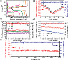
Figure 6. Electrochemical performance of the Li–S battery with a C@WS2/S composite electrode [74]. John Wiley & Sons. [Copyright © 2017 WILEY-VCH Verlag GmbH & Co. KGaA, Weinheim].
Download figure:
Standard image High-resolution imageThe use of WS2 as an anode material still has the following disadvantages: (a) large volume expansion and rapid capacity decay; and (b) low ion diffusion coefficient and conductivity response of the pure metal sulfide [76, 77]. One optimization method is the use of nanostructured WS2 materials that have a high specific surface area and short ion diffusion length [78]. Liu et al [79] synthesized WS2 nanowires with increased interlayer spacing by a simple solvothermal method. When the specific current was 100 mA g−1, the initial capacity of the WS2 nanowires was 605.3 mA h g−1. After 50 cycles, only 20% of the capacity was lost. Compared to bulk WS2, the layered structure and specific surface area of the WS2 nanowires considerably reduce the decay in the battery capacity. Another optimization method is to introduce WS2 into a carbon-containing matrix (e.g. carbon nanotubes, graphene or pyrolytic carbon), which can buffer large volume changes and improve the conductivity of the electrode [80]. Li et al [72] prepared WS2/C composites for application in sodium- and lithium-ion batteries. Carbon provides a good conductive substrate and buffers large changes in the volume of the WS2 material during the sodium-/lithium-ion intercalation/delamination process. Compared to the bare WS2, the synthesized WS2/C composite had a higher reversible specific capacity and improved cycle performance.
4.3.2. Solar cells.
With the global depletion of fossil-fuel resources, it is necessary to enhance the development and use of renewable energy. The energy conversion performed using solar cells contributes significantly to global renewable energy generation. The p–n junction in solar cells is formed by the window layer and the absorption layer. To achieve high optical throughput, the window layer needs to be thin, and it must have a high bandgap and low series resistance. The absorption layer must have a long carrier life, high electron mobility, and high absorption coefficient [81]. Owing to the unique optical, electronic and mechanical properties of 2D nanomaterials, they have recently been integrated with traditional bulk semiconductors to develop cost-effective solar cell devices. Among these materials, WS2 showed promising potential for application in solar cell devices. Optimizing the thickness of WS2 resulted in a direct bandgap > 2 eV and an indirect bandgap < 1.5 eV [82]. The optical absorption coefficient (>105cm−1) of WS2 is higher than that of the traditional three-dimensional Si semiconductor [83]. Therefore, WS2 has attracted the interest of researchers in the field of thin-film solar cell materials.
In 2017, Behura et al [84] synthesized a continuous large-area semiconductor with a 2D WS2 thin film on a three-dimensional p-Si solar-grade substrate using a three-zone low-pressure CVD system. Owing to the n-type conductivity of WS2, it has an atmospheric mass of 1.5 (aM 1.5G) that shows a good light response when connected to a p-Si bulk semiconductor. For the first time, Hussain et al [85] synthesized a large-area WS2/MoTe2 heterostructure on a conductive glass substrate and used it as the counter electrode of a dye-sensitized solar cell. Bin et al [86] used radio frequency (RF) magnetron sputtering to deposit a WS2 film on a soda-lime glass substrate. After analyzing the WS2 film prepared under different RF powers, they observed that an RF power of 200 W was suitable for using WS2 as a window layer material, with an optical bandgap of 2.2 eV and high visible light transmittance. Schottky-barrier solar cells have recently been used as photoactive materials owing to their relatively simple manufacturing process and low cost. Shanmugam et al [87] prepared a Schottky-barrier solar cell using a semiconductor WS2 nanofilm as the photoactive material in a layered structure. Its light conversion efficiency was 1.7% and its photon absorption capacity in the visible to the near-infrared spectral range was effective. Moreover, the layered device structure and the manufacturing process are relatively simple, and it is expected to be applied to solar cells.
4.4. Photodetectors
Photodetectors are sensitive to changes in their external environment and so they can be applied to flame detection, measurement control and video imaging. Presently, semiconductor materials (such as Si, GaN and InGaAs) are widely used in photodetectors for sensing spectral changes in the ultraviolet to infrared regions. However, traditional semiconductor thin-film materials, silicon nanomaterials, graphene and other functional materials have several inherent disadvantages. For example, the growth and processing of traditional semiconductor thin-film materials require high temperatures, which are unsuitable for the flexible polymeric substrates used for flexible photodetectors. In addition, the zero bandgap and low light absorption of graphene make it unsuitable for use in photodetectors. WS2 has a suitable bandgap and good thermal stability; hence, it is widely used in photodetectors.
Perea-López et al [88] used the CVD method for growing layered WS2 on a silicon substrate as a light sensor. The responsiveness of the device was only 97 μA W−1. Lan et al [89] synthesized WS2 monolayer films using an enhanced CVD method. However, the preparation and transmission processes of this enhanced method are very complicated. In addition, the area of the WS2 films produced is relatively small, which hinders their application in large-area photodetectors. To overcome these challenges, Li et al [90] used WS2 nanosheets to prepare novel large-area flexible photodetectors on filter membranes using a simple process. The photodetectors can respond to broadband wavelengths from 532 nm to 1064 nm. The bending resistance of the flexible photodetector was significant, as shown in figure 7, which shows the light response in a bending state. After 200 bending cycles, the photocurrent was 80% of the initial value.
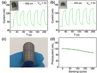
Figure 7. Bending resistance of the photodetectors prepared using WS2 nanosheets. Time-dependent optical response with a radius of curvature of (a) 0.75 cm and (b) 1.5 cm; (c) photodetector with manual bending; (d) photocurrent as a function of bending cycles. Reprinted from [90], Copyright (2020), with permission from Elsevier.
Download figure:
Standard image High-resolution image4.5. Lubricants
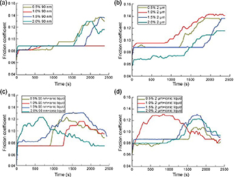
Micro- and nano-WS2 are excellent lubricating anti-friction materials, which can be used to solve the dynamic friction problems in the mechanical manufacturing of WS2. As the WS2 layers are connected by weak van der Waals forces, interlayer sliding easily occurs and the friction coefficient is low [91]. In 2018, Wu et al [91] compared the lubrication performance of a base oil, an ionic liquid (C7H11F3N2O3S) and WS2. Figure 8 shows the changes in the friction coefficients over time at a speed of 1450 rpm and under a constant load of 392 N. With increasing friction times, all friction coefficients increased, although those of the samples containing ionic liquids tended to decrease after peaking. In addition, the samples with WS2 and ionic liquids maintained their initial friction coefficient for a longer time compared to the base oil. Moreover, the addition of WS2 can significantly reduce the friction coefficient. This is because WS2 can be used as a solid or liquid lubricant. The micro-/nano-WS2 materials can be used in harsh working conditions, such as those involving high pressures, temperatures and loads, and in corrosive and radiative environments. Therefore, these materials are widely used in high-tech fields such as aviation and aerospace [92].
Figure 8. (a), (b) Friction coefficients of oil samples with different nano-/micro-WS2 (90 nm/2 μm) contents. (c), (d) Friction coefficients of the oil samples containing ionic liquids and different contents of nano-/micro-WS2 [91]. Reproduced from [91]. CC BY 4.0.
Download figure:
Standard image High-resolution image
In the automotive industry, efficient lubricants can increase the service life of various mechanical components. Aldana et al [93] studied the role of nano-WS2 as a lubricant additive for automotive gearboxes. After chemical analyses and transmission tests, they only observed W and S friction films on the gear surface; however, WS2 nanoparticles can enter the cracks and act as crack sealants, consequently reducing the propagation of cracks and preventing premature failure of mechanical parts. Huang et al [94] prepared self-lubricating WC–Ni–Cr-based composites containing WS2 using pulse current sintering at different temperatures and pressures. They observed that when the pressure exceeds 250 MPa and the sintering temperature is as low as 950 °C, the sintered composite material can be densified while preventing the decomposition of the disulfide. The tribological performance of the composites under sliding wear in air showed that the friction coefficient of high-pressure-sintered WS2 composites was lower than that of WC–Ni–Cr cermets without WS2. They inferred that wear debris accumulated in the low-lying areas of the wear surface and formed a discontinuity owing to self-lubrication by the WS2 layer, thereby reducing the friction coefficient.
4.6. Gas sensors
With the increasingly serious environmental problems, researchers are focusing on monitoring indoor and outdoor air quality. This has led to a considerable increase in research on gas sensors. However, fabricating gas sensors that are continuous and reliable, convenient and cheap is difficult. Previously, metal oxide semiconductors were typically used as sensing materials. Although their effect is good, most of the sensing needed to be carried out in high-temperature environments with a large amount of power, because they consume a significant amount of power. People are seeking new materials that can operate at low temperatures. WS2, an inorganic layered material whose structure is held together by van der Waals forces, is an appropriate material because of the following two reasons: (a) WS2 has a high specific surface area, and because the van der Waals forces are very weak, it has a large crystal spacing, which makes this structure suitable for a variety of interactions with the environment; (b) WS2 has a low bandgap and good conductivity; consequently, its working temperature is low [95].
In 2014, O'Brien et al [96] fabricated a WS2 gas sensor by sulfurizing a WO3 film at 500 °C using H2S plasma. Their study was the first to prove the gas-sensitive response of WS2 films and it is also an important attempt at low temperature detection. Subsequently, Järvinen et al [95] deposited a 20 nm thick metallic W film on the chip by sputtering and then sulfurized it in a quartz tube. At room temperature, the gas sensor was used to monitor H2, H2S, CO and NH3 in the air. WS2 had excellent selectivity to NH3 and high sensitivity (0.10 ± 0.02 ppm−1) Moreover. the sensor can respond to a stimulus quickly and recover quickly after the stimulus is removed.
4.7. Field-effect transistors
Because of its high switching current ratio, high thermal stability, electrostatic integrity [97] and the absence of dangling bonds, WS2 has been widely used in field-effect transistors. However, the electron mobility of single-layer WS2 is low, and researchers have proposed several methods to overcome this drawback. Iqbal et al [98] tried to use CVD to sandwich single-layer WS2 between hexagonal BN films and fabricated metal electrodes with Al and Au to achieve an ohmic contact. This scheme shows a very high mobility of 214 cm2 V s−1 at room temperature and it also avoids the hysteresis phenomenon of single-layer WS2. The hexagonal boron nitride film grown by CVD not only provides a stable platform for WS2 field-effect transistors but also acts as a protective layer against the external environment. In 2020, Zheng et al [99] reported for the first time a series of vertical heterostructures with high quality and a large area of WS2 (1−x) Se2x /SnS2 by two-step CVD. Based on the obtained structure, they successfully designed a dual-channel-type tunable field-effect transistor and the transition from a pure n-type unipolar transistor to a bipolar transistor was realized in this system.
5. Outlook
WS2 materials are used in many fields owing to their excellent SA characteristics, high carrier mobility, high flexibility, high optical absorption coefficient and suitable bandgap. This review has focussed on the recent progress in the use of WS2 for catalytic, laser, battery, photodetector and lubricant applications. Although significant progress has been made, research in this field is still in its infancy compared with the extensive exploration of carbon-based nanomaterials. Many fundamental properties of WS2 and issues related to its application have not yet been explored in detail. The current technology for preparing WS2 by physical methods is relatively mature, but it is difficult to effectively control the morphology, thickness and number of layers of WS2 films when preparing WS2 using chemical methods. For example, when using WS2 as an SA, optimization of its shape and thickness can increase the pulse energy of the laser. In addition, the fabrication of WS2 nanostructures is considered an effective way of improving the performance of WS2 in electrocatalysis, ion batteries and other applications. It is worth exploring the application of WS2 in other fields. Furthermore, composite materials should be investigated in more detail for specific applications; in particular, the material industry, as many experiments have shown that adding other substances to WS2 can effectively improve its performance. Finally, the promising performance of WS2 is expected to promote its application in new areas.
Acknowledgments
This work was financially supported by the National Natural Science Foundation of China (Grant No. 51801001), the China Postdoctoral Science Foundation (Grant No. 2016M601878), the Provincial Key Research and Development Program of Shaanxi (Grant No. 2019GY-197), the Key Project of Baoji University of Arts and Sciences (Grant No. ZK2018051), and the Natural Science Basic Research Plan in Shaanxi Province of China (Grant No. 2015JM5215). Feng AL is supported by The Thousand Talents Plan for Young Professionals of Shaanxi Province and High-level Leading Talents of Scientific and Technological Innovation of Baoji. We would like to thank Editage (www.editage.cn) for English language editing.