
Abstract
We experimentally studied three types of group-IV-semiconductor quantum-dots (IV-QDs) of Si-, SiC-, and C-QDs in a thermal SiO2 layer that were fabricated using a very simple hot-ion implantation technique for Si+, double Si+/C+, and C+ into the SiO2 layer, respectively, to realize a different wavelength photoluminescence (PL) emission from near-IR to near-UV ranges. TEM analyses newly confirmed both Si- and C-QDs with a diameter of approximately 2–4 nm in addition to SiC-QDs in SiO2. We successfully demonstrated very strong PL emission from three IV-QDs, and the peak photon energies (EPH) (peak PL-wavelength) of Si-, and SiC-, and C-QDs were approximately 1.56 eV (800 nm), 2.5 eV (500 nm), and 3.3 eV (380 nm), respectively. IV-QDs showed that the PL properties strongly depend on the hot-ion doses of Si and C atoms and the post N2 annealing processes. Consequently, it is easy to design peak PL wavelengths by controlling the ion doses of Si+ and C+ implanted into the SiO2 layer.
Export citation and abstract BibTeX RIS
1. Introduction
SiC semiconductors have been widely studied to evaluate the quantum phenomena of low-dimensional SiC structures as well as for realizing SiC power devices. 1) Although three-dimensional SiC is an indirect-bandgap structure, SiC can emit photoluminescent (PL) photons which are attributable to the free exciton recombination of electrons excited by photons in SiC. 2–4) The peak-PL photon energy (EPH) of SiC is equal to the exciton energy gap (EGX), which is approximately 0.1 eV lower than the bandgap energy (EG ). 2–4) Moreover, there are many diverse polytypes in SiC for which the physical properties including EGX, strongly depend on the polytype, 2,3) so it is possible that the peak-PL wavelength (λPL) of SiC photonic devices can be controlled by the polytype. Because the EG of SiC also depends on the diameter of SiC, 2) SiC nanostructures, 2)—such as a porous-SiC, 2,5–7) 2D-SiC, 2,8,9) SiC-nanowires, 2,10,11) and SiC-dots, 2,12,13)—are also candidates not only for materials science, including quantum effects, but also for photonic devices with various emission wavelengths.
Using the self-clustering effects of C atoms in a Si layer via hot-C+ ion implantation into Si, which was evaluated by atom probe tomography (ATP), 14–16) SiC nano-dots (dot-diameter Φ ≈ 2 nm) can be easily formed in various Si crystal structures from amorphous (a-Si) to crystal Si (c-Si) by a hot-C+-ion implantation technique performed in the wide ranges of Si-substrate temperature T and C+ ion-dose DC , that is, 500 ≤ T ≤ 1000 °C and 5 × 10¹² ≤ DC ≤ 7 × 1016 cm−2, 16–21) to evaluate the quantum mechanical phenomena in SiC-dots as well as to realize Si-based photonic devices. 22–24) The self-clustering effects of ion-implanted C atoms in Si leads to the local condensation of C-atoms with the diameter of several nm in Si layer, resulting in the local formation of SiC nano-dots in Si layers. 16,19,21) The hot-C+-ion implantation process can reduce the ion-implantation-induced damage to the Si layer, which is one of the advantageous characteristics of the hot-C+-ion implantation process. 18) Moreover, the partial formation of SiC-polytypes with different EGX values for cubic- (3C-SiC) and hexagonal-SiC (H-SiC) nano-dots were also confirmed both at the oxide/Si interface and in the Si layer, using corrector-spherical aberration transmission electron microscopy (CSTEM), high-angle annular-dark-field (HAADF) scanning transmission electron microscopy (STEM), and electron diffraction (ED) patterns that were obtained by fast Fourier transform (FFT) analysis of the lattice spots of CSTEM data. 16) As a result, we demonstrated a broad photoluminescence (PL) spectrum with very strong emission intensity (IPL) from the visible to the near-UV regions (>400 nm) even from indirect-bandgap SiC-dots, for which the IPL is two orders of magnitude larger than that of 2D-Si. 25–26)
Because the SiC dots that have a larger EG (>2.4 eV) embed in the Si layer that has a smaller EG (≈1.1 eV), 27) the SiC-dots in the Si layer are not quantum-dot (QD), resulting in a very small PL quantum efficiency for visible Si-based photonic devices. Thus, we experimentally realized SiC-QDs embedded in SiO2 with a large EG of 9 eV, 27) using the simple processes of implanting double hot-Si+/C+-ion into a SiO2 layer and post N2 annealing at 1000 °C. 28) HAADF-STEM observation showed that the SiC-QD diameter and density were approximately 2 nm and 1.5 × 1012 cm−2, respectively, and the clear lattice spots of some SiC-QDs were also verified by CSTEM. 28) Moreover, after N2 annealing, the PL intensity of SiC-QDs rapidly increased, and as a result, we successfully confirmed that the PL quantum efficiency of SiC-QDs was approximately 2.5 times greater than that of SiC-dots in the Si layer because of the increased life time of excited electrons, which are quantum mechanically confined in SiC-QDs. 28) Thus, the post N2 annealing is also a key process for forming SiC-QDs. In addition, to realize different wavelength photonic devices from IR to UV ranges, QD structures with various EG values, such as Si-and C-QDs as well as SiC-QDs, are also needed. Si- 29,30) and C-QDs 31) have been widely studied, but they have not yet been realized via the easy and simple processes of hot-ion implantation and the post N2 annealing techniques.
In this work, we experimentally studied the group-IV-semiconductor QDs (IV-QDs) embedded in the SiO2 layer—Si-, SiC-, and C-QDs—using very simple processes of both hot-ion implantation into the SiO2 layer and post N2 annealing. 32) Many QD formations of Si- and C-atoms in addition to SiC in SiO2 layer were successfully confirmed by HAADF-STEM, and some IV-QDs also showed clear lattice spots when observed by CSTEM. We successfully demonstrated very strong PL emissions with different peak photon energies EPH values from Si-QDs (near-IR) fabricated by Si+ hot-implantation, SiC-QDs (visible range) fabricated by double Si+/C+ hot-implantation, 28) and C-QDs (near-UV) fabricated by C+ hot-implantation.
2. Experimental procedures
Using the simple fabrication processes of the hot-ion implantation into a thermal surface-SiO2 layer (SOX) before post N2 annealing, 28) we realized three types of IV-QDs (Si-, SiC-, and C-QDs) in a SiO2 layer. Figure 1 shows the fabrication steps for IV-QDs, and Table I shows the process conditions for hot-ion implantation and temperature T for each IV-QD. Figure 1(b) shows that IV-QDs were fabricated by hot-ion implantation conditions shown in Table I into the 140 nm thick SiO2 layer (SOX) on the (100) bulk-Si substrate at T, after the SOX was formed via the dry O2 oxidation of (100)-Si, as shown in Fig. 1(a). Table I shows that Si-, SiC- and C-QDs were fabricated by single-Si+, double-Si+/C+, and single-C+ hot-ion implantations, respectively, where 200 ≤ T ≤ 900 °C, and the hot-ion dose conditions of Si+ (DS ) and C+-ion doses (DC ) were varied from 4 × 10¹⁶ to 1 × 1017 cm−2 with the ion projection range of the middle of SiO2 layer to realize a higher PL intensity of IV-QDs. The acceleration energies of the Si+ and C+ ions were 60 and 25 keV, respectively, for which the projection range was the middle of the SiO2 layer. For SiC-QDs, the DS /DC ratio dependence of the PL properties was also studied, although our previous study 28) showed that the optimum DC condition for realizing higher IPL of SiC-QDs was 4 × 1016 cm−2. Figure 1(c) shows that the post N2 annealing was carried out at an annealing temperature of TN = 1000 °C for various annealing times tN (0 ≤ tN ≤ 120 min) to recover the crystal quality of the IV-QDs.
Fig. 1. (Color online) IV-QD fabrication steps via hot-ion-implantation into SiO2 layer. After (a) dry-oxidation process of bulk-Si substrate at 1000 °C (oxide thickness TOX = 140 nm), (b) hot-ions were implanted into SiO2 layer at T. (c) Post N2 annealing was carried out at TN of 1000 °C for tN . Process conditions for (b) are shown in Table I.
Download figure:
Standard image High-resolution imageTable I. Process conditions of hot-ion temperature T and ion doses of Si (DS ) and C (DC ) for Si-, SiC- and C-QDs.
| QD-type | Hot-ions | DS (×1016 cm−2) | DC (×1016 cm−2) | T (°C) |
|---|---|---|---|---|
| Si | Si+ | 6–10 | 600 | |
| SiC | Si+/C+ | 4–8 | 4 | 200–900 |
| C | C+ | 4–10 | 400–600 |
The PL and Raman properties of IV-QDs were measured at room temperature, at which the excitation laser energy, power, and diameter were 3.8 eV, 0.6 mW, and 1 μm, respectively. The broad-wavelength (λPL) PL spectrum from the near-UV to near-IR regions was calibrated using a standard illuminant.
3. Results and discussion
3.1. Material structures of IV-QDs
The depth profiles of implanted Si at DS = 6 × 1016 cm−2 and C-atom concentrations at DC = 4 × 1016 cm−2 in IV-QDs, after N2 annealing, were evaluated by the Si2p and C1s spectra of X-ray photoelectron spectroscopy (XPS), respectively, as shown in Fig. 2(a). The XPS accuracies for the content and depth positions were ±1 at% and ±2 nm, respectively, and the X-ray beam diameter was 100 μm. 21) The peak Si- and C-concentrations in the SiO2 layer were approximately 6 × 10²¹ and 4 × 1021 cm−3, respectively. Because the Si- and C-peak concentrations are proportional to DS and DC , the maximum Si at DS = 1 × 1017 cm−2 and C concentrations at DC = 1 × 1017 cm−2 in this work were estimated to be the same as 1 × 1022 cm−3 in SiO2. Moreover, Fig. 2(b) shows the depth profiles of the C-contents of the Si−C and C–C bonds in SiC-QDs at T = 200 °C (solid line) and 600 °C (dashed line), and the C-contents are nearly independent of T despite a changing 400 °C of T. Thus, Fig. 2(b) suggests that the effect of T on the C-contents of Si−C and C–C bonds is very small within a large area of 100 μm in diameter, which is similar to the results for the SiC-dots in the Si layer. 21) However, the influence of T on the SiC-QD properties will be discussed in Fig. 5(c).
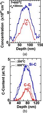
Fig. 2. (Color online) (a) Concentration depth-profiles of implanted Si (solid line) at DS = 6 × 1016 cm−2 or C (dashed line) atoms at DC = 4 × 1016 cm−2 in SiO2 layer, which was evaluated by Si2p and C1s spectra of XPS, respectively, where T = 600 °C, TN = 1000 °C, and tN = 30 min. (b) T dependence of C-content depth profiles of Si–C (blue lines) and C–C bonds (red lines) in double Si+/C+ ion implanted SiO2 layer at tN = 30 min, where solid and dashed lines show the data at T = 200 °C and 600 °C, respectively. Concentration accuracy evaluated by XPS was estimated to be ±1 at%, depth error bar was approximately ±2 nm, and X-ray beam diameter of XPS was 100 μm. Figure 2(a) shows that the peak concentrations of Si and C atoms were approximately 6 × 10²¹ and 4 × 1021 cm−3, respectively, in the middle of SiO2 layer. Figure 2(b) shows that the C-contents of Si–C and C–C bonds are almost independent of T.
Download figure:
Standard image High-resolution imageNext, we discuss the IV-QD structures as evaluated using electron microscopes. We experimentally confirmed many Si- and C-QDs, in addition to SiC-QDs, using HAADF-STEM observations, as shown in Figs. 3(a)−3(d). Figures 3(a) and 3(b) shows the whole SOX area and the SOX middle area of SiC-QDs, respectively, where DS = 6 × 1016 cm−2, T = 600 °C, and tN = 60 min. Si-QDs were uniformly formed in the middle SOX area with an 80 nm width of higher Si concentration region [>2.5 × 1021 cm−3 in Fig. 2(a)], but Fig. 3(a) shows that in the surface and bottom areas of SOX with lower Si concentration, few Si-QDs could be observed. This may be attributable to the detection limitation of HAADF-STEM, that is, it is possible that the Φ of the Si-QDs in the lower Si concentration region is too small to be detected by HAADF-STEM. We also confirmed the similar depth distributions of other SiC- and C-QDs with higher dopant regions. Figures 3(c) and 3(d) also shows that other SiC- at DS = 6 × 1016 cm−2, DC = 4 × 1016 cm−2, and T = 400 °C as well as C-QDs at DC = 1 × 1017 cm−2 and T = 400 °C were uniformly formed in the middle areas of the SOX layer with higher dopant concentrations, respectively. In addition, the diameter Φ and surface density N of the IV-QDs also depend on the type of IV-QDs.

Fig. 3. (Color online) HAADF-STEM images of successful formation of many Si-QDs (encircled bright spot) in (a) whole SOX area and (b) SOX middle-area at DS = 6 × 1016 cm−2, T = 600 °C, and tN = 60 min; (c) SiC-QDs (encircled bright spot) at DS = 6 × 1016 cm−2, DC = 4 × 1016 cm−2, T = 400 °C, and tN = 60 min, and (d) C-QDs (encircled dark spot) at DC = 1 × 1017 cm−2, T = 400 °C, and tN = 30 min. Figure 3(a) shows that Si-QDs were uniformly formed in middle SOX area with 80 nm width in higher Si concentration region [>2.5 × 1021 cm−3 in Fig. 2(a)], but in the surface and bottom areas of SOX with lower Si concentrations, few Si-QDs were observed. Figures 3(b)–3(d) shows that all IV-QDs were uniformly formed in middle areas of SOX layer, but their sizes vary slightly. QD surface density also depends on type of IV-QDs.
Download figure:
Standard image High-resolution imageFigures 4(a) and 4(b) shows the Φ histogram of Si-QDs and the normal probability plot of Φ as those used in Fig. 3(b), respectively. The average Φ and standard deviation of Φ (σΦ) of Si-QDs were 2.37 and 0.28 nm, respectively. Moreover, Fig. 4(b) shows that the Φ distribution can be explained by the Gaussian function (solid line). The Φ distribution of other IV-QDs was also confirmed by the Gaussian function, which indicates that the Φ of the IV-QDs randomly fluctuates. As a result, the σΦ of Si-QDs (≈0.28 nm) was much smaller than the σΦ of SiC- and C-QDs (≈1.0 nm), which may be caused by the diffusion difference between Si and C atoms in SiO2. We will discuss the effect of N2 annealing on the Φ of Si-QDs. Because the Si-diffusivity dS
in SiO2 is reported to be dS
= 1.38 exp (−4.74 eV/kT) cm2 s−1,
33) where k denotes the Boltzmann constant and the diffusion length (LD
≡  )
27) of Si is estimated to be approximately 0.4 nm at TN
= 1000 °C and tN
= 30 min. Therefore, the LD
/Φ of Si-QDs is approximately 17% and is in almost the same order as σΦ. This LD
increase after N2 annealing could not be observed using HAADF-STEM, because the Si-QD image at tN
= 0, which is considered to be small, could not be observed under the detection limitations of HAADF-STEM.
28)
)
27) of Si is estimated to be approximately 0.4 nm at TN
= 1000 °C and tN
= 30 min. Therefore, the LD
/Φ of Si-QDs is approximately 17% and is in almost the same order as σΦ. This LD
increase after N2 annealing could not be observed using HAADF-STEM, because the Si-QD image at tN
= 0, which is considered to be small, could not be observed under the detection limitations of HAADF-STEM.
28)

Fig. 4. (Color online) (a) Histogram of Φ of Si-QDs in 5000 nm2 area, and (b) normal probability plot of Φ of Fig. 4(a) (circles). Process conditions of IV-QDs are the same as those in Fig. 3. Figure 4(a) shows that average Φ and σΦ of Si-QDs are approximately 2.37 nm and 0.28 nm, respectively. Figure 4(b) shows that Φ distribution of (a) can be explained by the Gaussian function (solid line).
Download figure:
Standard image High-resolution imageHere, we summarize the Φ and N for each type of IV-QDs, using the data in Fig. 3. Figure 5(a) shows the average Φ and N for each of the three types of IV-QDs evaluated by the HAADF-STEM data shown in Fig. 3. N was determined by the number of QDs (n) over the cross section area (SCS) shown in Fig. 3, that is, N = n/SCS. The average Φ of the IV-QDs varied from approximately 2–4 nm, and the average Φ of the Si-QDs was the smallest among the three IV-QDs. Moreover, the N of the Si-QDs was the highest of the three IV-QDs, and the IV-QD surface densities were approximately 2 × 1012 cm−2 with an error bar of 20%. The error bars of Φ and N in Fig. 5 showed the σΦ and the statistical deviation of N (δN), respectively, where δN/N is given by the statistical deviation of n, that is, δN/N =  assuming that n randomly fluctuates.
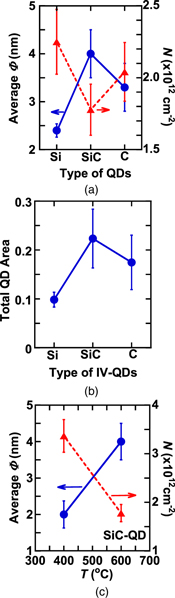
Fig. 5. (Color online) (a) Average Φ (circles) and N (triangles) and (b) total QD area SQD in a unit area obtained by SQD = Nπ(Φ/2)2 as a function of the type of IV-QDs of Si-, SiC-, and C-QDs, where the process conditions are the same as those in Fig. 4(c). (c) T dependence of average Φ and N in SiC-QDs, where DS = 6 × 1016 cm−2, DC = 4 × 1016 cm−2, and tN = 60 min. Figure 5(a) shows that the Φ and N strongly depend on the type of IV-QD. Φ varies from 2 to 4 nm in IV-QDs, and σΦ of Si-QDs, shown as an error bar, is small (≈0.28 nm), but σΦ of SiC- and C-QDs is relatively large (≈1.0 nm). N of IV-QDs was approximately 2 × 1012 cm−2 with standard deviation of approximately 20%, as shown in error bars. In addition, the N increases with decreasing Φ. Figure 5(b) shows that the SQD of IV-QDs varies from approximately 0.1–0.2, and maximum variation of δSQD/SQD calculated by Eq. (2) is approximately ±31% in SiC-QDs. Figure 5(c) shows that with decreasing T, the Φ of SiC-QDs decreases, but N increases.
Download figure:
Standard image High-resolution imageWe discuss the total QD area (SQD) of IV-QDs in the SiO2 layer, because the PL intensity (IPL) of the QDs is proportional to SQD, as shown in Eq. (1), 28) where SQD = Nπ(Φ/2)2, assuming that the QDs are spheres.

where η and I0 denote the PL emission coefficient of IV-QDs and the excited laser flux at the surface SiO2. The penetration length of laser photons with 3.8 eV in the SiO2 layer can be assumed to be infinite, because the EG of SiO2 (9 eV) 28) is much higher than the laser photon energy of 3.8 eV. Moreover, the SQD variation δSQD can be given by the following equation:
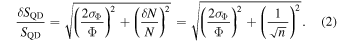
Figure 5(b) shows the estimated SQD per unit area and δSQD/SQD of the three types of IV-QDs, respectively, using the data in Fig. 5(a). The SQD of IV-QDs varies from approximately 0.1–0.2, which slightly depends on the type of IV-QDs. Equation (1) indicates that the SQD is considered to affect the PL properties, as discussed in Sect. 3.3. The maximum δSQD/SQD is approximately ±31% in SiC-QDs, because of the lower N of SiC-QDs shown in Fig. 5(a).
Figure 5(c) shows the T dependence of the average Φ and N in SiC-QDs, where DS = 6 × 1016 cm−2, DC = 4 × 1016 cm−2, and tN = 60 min. With increasing T, the average Φ increases, but N decreases, which is the similar to the results for the SiC-dots in the Si layer. 21) Therefore, even after N2 annealing, we confirmed the influence of T on the SiC-QD formation, which may be attributable to the SiC-QD growth by gathering small SiC-QDs during the high-T hot-ion implantation process.
Next, we discuss the crystal structures of the IV-QDs, using the lattice spots of IV-QDs evaluated by CSTEM. Figures 6(a-1), 6(b-1), 6(c-1), and 6(d) shows the CSTEM images of the cross section of Si-, H-SiC-, 3C-SiC- and C-QDs in SiO2 (encircled areas) under the same process conditions as those in Fig. 3. All three IV-QDs show clear lattice spots, confirming that some Si- and C-QDs also consist of crystal structures. Figures 6(a-2), 6(b-2), and 6(c-2) shows the ED patterns of [111]Si with lattice spaces d = 0.314 nm, ![$\left[10\overline{1}3\right]$](https://content.cld.iop.org/journals/1347-4065/60/SB/SBBK08/revision7/jjapabdb80ieqn3.gif) H-SiC with d = 0.237 nm, and (111) 3C-SiC with d = 0.251 nm, as evaluated by FFT analysis of the lattice spots of Figs. 6(a-1), 6(b-1), and 6(c-1), respectively. As a result, it was found that SiC-QDs also consist of 3C- and H-SiC polytypes, although it has already been confirmed
16,19,21) that SiC-dots in the Si layer consist of 3C- and H-SiC polytypes. In contrast, the lattice distance of the C-atoms in Fig. 6(d) was approximately 0.36 nm, which is nearly equal to the layer distance of graphite (≈0.335 nm).
34) Thus, some C-QDs consist of nano-graphite with a diameter of approximately 2 nm, as indicated by the G- and D-bands of the UV-Raman spectroscopy shown in Fig. 7(b). However, all IV-QDs, as confirmed by the HAADF-STEM images in Figs. 3(a)−3(c), showed no clear lattice spots. For example, only 1/4 of the Si-QDs, confirmed by HAADF-STEM, shows clear lattice images via CSTEM. Therefore, the crystal quality of some IV-QDs is poor, which suggests that some part of C-QDs consist of a-C. Consequently, IV-QDs consist of both amorphous and crystal structures.
H-SiC with d = 0.237 nm, and (111) 3C-SiC with d = 0.251 nm, as evaluated by FFT analysis of the lattice spots of Figs. 6(a-1), 6(b-1), and 6(c-1), respectively. As a result, it was found that SiC-QDs also consist of 3C- and H-SiC polytypes, although it has already been confirmed
16,19,21) that SiC-dots in the Si layer consist of 3C- and H-SiC polytypes. In contrast, the lattice distance of the C-atoms in Fig. 6(d) was approximately 0.36 nm, which is nearly equal to the layer distance of graphite (≈0.335 nm).
34) Thus, some C-QDs consist of nano-graphite with a diameter of approximately 2 nm, as indicated by the G- and D-bands of the UV-Raman spectroscopy shown in Fig. 7(b). However, all IV-QDs, as confirmed by the HAADF-STEM images in Figs. 3(a)−3(c), showed no clear lattice spots. For example, only 1/4 of the Si-QDs, confirmed by HAADF-STEM, shows clear lattice images via CSTEM. Therefore, the crystal quality of some IV-QDs is poor, which suggests that some part of C-QDs consist of a-C. Consequently, IV-QDs consist of both amorphous and crystal structures.
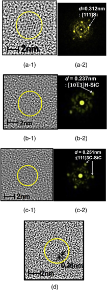
Fig. 6. (Color online) CSTEM lattice images of cross sections of (a-1) Si-QD, (b-1) H-SiC-QD, (c-1) 3C-SiC-QD, (d) C-QD, and ED-patterns of (a-2) [111]Si-QD, (b-2) H-SiC-QD, and (c-2) 3C-SiC-QD evaluated by FFT analyses of (a-1), (b-1), and (c-1), in which the process conditions are the same as Fig. 3. Lattice spaces of 0.237 nm of (b-2) and 0.251 nm of (c-2) indicate that polytypes of SiC-QD of (b-1) and (c-1) are ![$\left[10\bar{1}3\right]$](https://content.cld.iop.org/journals/1347-4065/60/SB/SBBK08/revision7/jjapabdb80ieqn4.gif) H-SiC and (111) 3C-SiC, respectively. Lattice distance of C-QD in (d) was approximately 0.36 nm, which is nearly equal to the layer distance of graphite (≈0.335 nm).
34)
H-SiC and (111) 3C-SiC, respectively. Lattice distance of C-QD in (d) was approximately 0.36 nm, which is nearly equal to the layer distance of graphite (≈0.335 nm).
34)
Download figure:
Standard image High-resolution image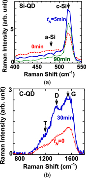
Fig. 7. (Color online) tN dependence of UV-Raman spectrum of (a) Si-QD at DS = 6 × 1016 cm−2, and (b) C-QD at DC = 1 × 1017 cm−2, where T = 600 °C. Arrows in (a) show the peak Raman positions of c-Si (520 cm−1), including Raman intensity from Si-substrate under SOX layer and a-Si in Si-QDs (480 cm−1). After N2 annealing, peak Raman intensity of c-Si increases, but the peak Raman intensity of a-Si decreases. Arrows in (b) show T (a-C), D, and G bands of graphite, and after N2 annealing, all peak-Raman intensities of graphite also increase.
Download figure:
Standard image High-resolution imageAs an example of a Si-QD for which the crystal structure is clear, we estimate the Si atom number of Si-QDs observed by HAADF-STEM data in Figs. 5(a)−5(b), compared with that vis the XPS data shown in Fig. 2(a). First, we estimate the Si atom number of the Si-QDs NQD using Eq. (3).

where NSi is the Si volume density (≡5 × 1022 cm−3), 27) SQD ≈ 0.1 in Fig. 5(b), and W denotes the depth width of the Si-QD formation area (≈80 nm) shown in Fig. 3(a), resulting in NSD ≈ 4 × 1016 cm−2.
In contrast, the Si atom number via the XPS data in Fig. 2(a); NXPS was obtained by integrating the depth profile of the Si atom profile with more than 2.5 × 1021 cm−3 of the Si-QD formation area shown in Fig. 3(a), resulting in NXPS ≈ 3.6 × 10¹⁶ ± 0.5 × 1016 cm−2. Thus, NSD ≈ NXPS within an XPS accuracy of 1 at%. Consequently, we confirmed that approximately 100% of the Si atoms evaluated by XPS data form Si-QDs, as observed by HAADF-STEM in Fig. 3(a).
3.2. UV-Raman properties of IV-QDs
In this subsection, we discuss the material properties of the IV-QDs evaluated by UV-Raman spectroscopy. Figures 7(a) and 7(b) shows the tN dependence of the UV-Raman spectrum of Si- at DS = 6 × 1016 cm−2 and C-QDs at DC = 1 × 1017 cm−2, respectively, where T = 600 °C. The arrows in Fig. 7(a) show the peak Raman shifts of c-Si (520 cm−1), including the Raman intensity IR0 from the Si-substrate under the SOX layer, in addition to a-Si in Si-QDs (480 cm−1). The peak Raman intensity of c-Si increases and the a-Si Raman peak decreases after N2 annealing, where the measured c-Si Raman intensity minus IR0 (≡ΔIR ) shows the net Si-Raman intensity of Si-QDs in SiO2. Thus, the crystal quality of Si-QDs can be improved via N2 annealing. Moreover, the arrows in Fig. 7(b) show the T-, D-, and G-bands of C–C vibrations in C-QDs. After N2 annealing, the peak Raman intensities of the G- and D-bands increased, but the N2 annealing effect on the T-band intensity was small. Thus, the graphite component of C-QDs, which was already confirmed via CSTEM, as shown in Fig. 6(c), also increases after N2 annealing. Our previous work 28) on the tN dependence of UV-Raman analysis for SiC-QDs also demonstrated that the peak-Raman intensities of the D-, T-, and TO-modes of Si−C vibration increase after a brief N2 annealing, which leads to the improvement of the quality of the SiC-QDs.
Figure 8(a) shows the UV-Raman spectra of SiC-QDs as a function of the DS /DC dose ratio at a fixed DC of 4 × 1016 cm−2, where T = 200 °C and tN = 0. The arrows in Fig. 8(a) show the G-, D-, and T-bands, which are attributable to the separated C atom areas in SiO2, 28) and the TO mode of the Si−C vibration. The Raman spectrum line shape strongly depends on DS /DC even at the same DC . The G band can be observed at DS /DC ≤ 1.5. Moreover, Fig. 8(b) shows the peak Raman intensities of the D- and TO-bands versus DS /DC at the same data used in Fig. 8(a). The D-band intensity increases with decreasing DS /DC , which suggests that the separated C atoms in SiO2 increase at low DS conditions. The TO intensity is reduced only at DS /DC = 2. Thus, the Si−C bond formation shown by the TO-mode increases with decreasing DS , so this study indicates that DS /DC ≤ 1.5 is optimum for forming SiC in this study.

Fig. 8. (Color online) DS /DC -ratio dependence of (a) UV-Raman spectrum and (b) peak TO- and D-band intensities of SiC-QD, where DC = 4 × 1016 cm−2, T = 200 °C, and tN = 0. Arrows in Fig. 8(a) show G, D and T bands of C–C vibrations, and TO mode of Si–C vibration. Figure 8(a) shows that Raman spectrum line shape strongly depends on DS /DC . Figure 8(b) shows that peak Raman intensities of D- and TO-bands increase with decreasing DS /DC .
Download figure:
Standard image High-resolution image3.3. PL properties
3.3.1. QD type dependence
In this subsection, we discuss the PL properties as a function of the type of IV-QDs. Figure 9(a) shows the PL spectrum comparison among three types of IV-QDs: Si-QDs (solid line: DS = 6 × 1016 cm−2, T = 600 °C, tN = 1.5 h), SiC-QDs (dashed line: DS = 6 × 1016 cm−2, DC = 4 × 1016 cm−2, T = 200 °C, tN = 30 min), and C-QDs (dotted line: DC = 1 × 1017 cm−2, T = 600 °C, tN = 30 min) after N2 annealing, in which the PL intensity of SiC-DQ is reduced to 1/3 of measured PL data. The lower and upper axes show the PL photon energy and wavelength λPL, respectively. We experimentally demonstrated the PL emissions from three types of IV-QDs with different peak-PL energy EPH (peak-λPL) emissions from Si-QDs (near-IR), SiC-QDs (visible region), and C-QDs (near-UV). Thus, the PL spectrum line shape and IPL strongly depend on the type of IV-QDs, and the EPH (peak-λPL) of Si-, and SiC-, and C-QDs were approximately 1.56 eV (800 nm), 2.42 eV (500 nm), and 3.28 eV (380 nm), respectively. The IPL of the SiC-QDs was the largest and was approximately 2.6 and 6.6 times greater than that of Si- and C-QDs, respectively. Moreover, the Si-QDs showed a very sharp PL spectrum with a FWHM of 0.36 eV, compared with the broad FWHM of SiC- (0.85 eV) and C-QDs (0.89 eV). The broad PL spectrum of SiC-QDs can be explained by the PL components of cubic and hexagonal SiC-polytypes with different EGX, as discussed in Fig. 15. Consequently, it is easy for IV-QDs to control PL emission wavelength from near-IR to near-UV by changing the type of atoms implanted into the SiO2 layer. The PL emission mechanisms for SiC- and Si-QDs are attributable to the sum of the emissions from various SiC polytypes as shown in Fig. 15, and the quantum-mechanically induced EG -expansion of Si-QDs which are indicated in Fig. 11(b), respectively. However, the physical mechanism for C-QD emission is not currently understood, but it may be caused by the photon emissions from a-C and nano-graphite. 31,34) Moreover, Fig. 9(b) shows the T dependence of the maximum IPL (IMAX) of SiC-QDs (squares) and C-QDs (triangles) at the same ion dose conditions in Fig. 9(a). The IMAX of SiC-QDs drastically increases with decreasing T, but the IMAX of C-QDs slightly increases with increasing T. As a result, the optimum T conditions for realizing the strongest IMAX of SiC- and C-QDs are 200 and 600 °C, respectively. This T dependence of SiC-QDs could be attributable to the N increase in the SiC-QDs at lower T conditions. 28) Therefore, we will discuss the PL data of SiC- and C-QDs under the optimum T conditions shown in Fig. 9(b).
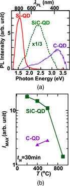
Fig. 9. (Color online) (a) PL spectrum comparison among three IV-QDs of Si-QD (solid line: DS = 6 × 1016 cm−2, T = 600 °C, tN = 1.5 h), SiC-QD (dashed line: DS = 6 × 1016 cm−2, DC = 4 × 1016 cm−2, T = 200 °C, tN = 30 min), and C-QD (dotted line: DC = 1 × 1017 cm−2, T = 600 °C, tN = 30 min). Lower and upper axes show the PL photon energy and wavelength, respectively. The PL intensity of SiC-DQ is reduced to 1/3 of measured PL data. PL spectrum strongly depends on type of IV-QDs, and very different EPH (peak-λPL) values were realized among three IV-QDs. EPH (peak-λPL) of Si-, and SiC-, and C-QDs were approximately 1.56 eV (800 nm), 2.42 eV (500 nm), and 3.28 eV (380 nm), respectively. (b) T dependence of IMAX of SiC-QDs (squares) and C-QDs (triangles) under the same ion dose conditions as those shown in Fig. 9(a). Figure 9(b) shows that optimum T conditions for increasing IMAX of SiC- and C-QDs are 200 °C and 600 °C after N2 annealing, respectively.
Download figure:
Standard image High-resolution imageNext, we address the effect of N2 annealing on the PL properties of IV-QDs. Figures 10(a)–10(c) shows the tN dependence of the PL spectra of the Si-, SiC-, and C-QDs, respectively, where the process conditions of IV-QDs are the same as those in Fig. 9. The PL spectrum line shape of each IV-QD after N2 annealing is mostly independent of tN . However, the IPL drastically increases with increasing tN , but the IPL increase factors of N2 annealing are also affected by the type of IV-QDs. The IPL of the three IV-QDs rapidly increases after short N2 annealing, and in particular, the tN dependence of the IPL of Si-QDs continues to grow larger with increasing tN even for long tN value.
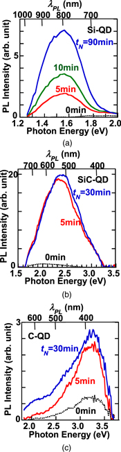
Fig. 10. (Color online) tN dependence of PL spectrum of (a) Si-, (b) SiC-, and (c) C-QDs, where process conditions of IV-QDs are the same as those seen in Fig. 9. PL spectrum line shape of each IV-QD is nearly independent of tN , but PL intensity of each QDs increases with increasing tN .
Download figure:
Standard image High-resolution imageWe summarize the tN
dependence of the PL properties of IV-QDs. Figures 11(a) and 11(b) shows the tN
dependence of the IMAX and EPH (peak-λPL) under the same process conditions in Fig. 9, respectively, where circles, squares, and triangles show the data of Si-, SiC-, and C-QD, respectively, and the right vertical axis in Fig. 11(b) shows the peak PL wavelength (peak-λPL). The rhombi in Fig. 11(a) show the data of SiC dots in the Si layer at DC
= 4 × 1016 cm−2 and T = 600 °C. Both the IMAX and EPH (peak-λPL) of IV-QDs strongly depend on the type of IV-QDs. The IMAX of IV-QDs rapidly increased after a brief N2 annealing, which could be attributable to the improved crystal quality of IV-QDs, as shown by the Raman data of IV-QDs in Figs. 7(a) and 7(b). The maximum IMAX enhancement factors of Si-, SiC-, and C-QDs, compared to IMAX at tN
= 0, reached approximately 59, 23, and 3.3, respectively, which indicates that post N2 annealing is also a key process in realizing a higher IPL. Thus, the IMAX enhancement factor of Si-QDs is at its maximum in the three IV-QDs. In addition, even during high-TN
annealing, the IMAX of IV-QDs continues to increase with increasing tN
. However, Fig. 11(a) shows that SiC-dots in the Si layer show a drastic decrease in IMAX with increasing tN
, that is,  where tD
is a decay scaling time of approximately 21 min.
21) Thus, the SiC-dot structures in the Si layer are thermally unstable at high TN
conditions, which may be caused by the decomposition of SiC during high-TN
annealing.
21) Consequently, IV-QD structures have thermal stability even at a higher TN
, which is an advantageous characteristic of IV-QDs in the SiO2 layer.
where tD
is a decay scaling time of approximately 21 min.
21) Thus, the SiC-dot structures in the Si layer are thermally unstable at high TN
conditions, which may be caused by the decomposition of SiC during high-TN
annealing.
21) Consequently, IV-QD structures have thermal stability even at a higher TN
, which is an advantageous characteristic of IV-QDs in the SiO2 layer.

Fig. 11. (Color online) tN dependence of (a) IMAX, and (b) EPH (left vertical-axis) and peak-λPL (right vertical-axis) at the same data of Fig. 9 [Si-QD (circles), SiC-QD (squares), and C-QD (triangles)]. Rhombi in Fig. 11(a) show the data of SiC dots in c-Si layer at DC = 4 × 1016 cm−2 and T = 600 °C. IMAX of three IV-QDs rapidly increases after a brief N2 annealing and continues increasing with increasing tN . However, only SiC dots in c-Si layer decrease with increasing tN under tN ≥ 5 min. As shown in Fig. 11(b), only SiC-QDs shows the rapid increase of EPH after a brief N2 annealing, because 3C-SiC, which have an EGX = 2.39 eV, was formed. However, the EPH of other IV-QDs is nearly independent of tN . Figures 11(a) and 11(b) show that both the IMAX and EPH (peak-λPL) of IV-QDs strongly depend on the type of IV-QDs. The IMAX of SiC-QDs is approximately 2.6 and 6.6 times greater than that of Si- and C-QDs, respectively. Consequently, the EPH of IV-QDs varies from 1.56 to 3.28 eV, that is, peak-λPL of IV-QDs varies from 380 to 800 nm.
Download figure:
Standard image High-resolution imageFigure 11(b) shows that different peak-λPL values for a near-IR of 800 nm to a near-UV of 380 nm can be obtained only by changing the type of IV-QDs. Moreover, only SiC-QDs showed strong tN dependence on EPH, because the EPH increase from 2.0 eV of Si–C alloy at tN = 0 to 2.3 eV at tN = 5 min could be attributable to the 3C-SiC (EGX = 2.39 eV) QD-formation that occurs by binding the Si–C atoms during high-TN annealing for tN = 5 min. 28) Because Fig. 5(a) shows that the Φ of SiC-QDs is approximately 4 nm and relatively large, and in addition, the quantum-mechanics effects on EG expansion (EG ∝ Φ−2) in SiC-QDs occurs in Φ < 3 nm, 2) the quantum-mechanical effects on EG expansion of SiC-QDs in this study was very small. On the other hand, Fig. 11(b) shows that the EPH of Si-QDs with Φ ≈ 2.5 nm [as shown in Fig. 5(a)] was 1.56 eV, which is nearly equal to the reported experimental results reached in EG via quantum EG -expansion of Si-QDs at Φ ≈ 3 nm. 35) In addition, considering the long tailing of the PL spectrum of Si-QDs at the half-width-tenth-maximum (HWTM), shown in Figs. 9 and 10(a), the HWTM of EPH in Si-QDs (δEPH) was approximately 0.28 eV. Assuming that the δEPH is attributable to the quantum EG -expansion of EG ∝ Φ−2, this δEPH is caused by the σΦ shown in Fig. 5(a), so δEPH/EPH can be given by Eq. (4)

Therefore, the experimental δEPH/EPH seen in Fig. 9 was approximately 0.18, and the δEPH/EPH obtained by substituting the experimental σΦ/Φ of 0.12 in Fig. 5(a) into Eq. (4) was 0.24, which is neatly equal to the experimental δEPH/EPH. As a result, Eq. (4) is nearly valid in Si-QDs, so the HWTM of the PL spectrum in Si-QDs is also attributable to the statistical variation of the Si-QD diameter. Thus, for Si-QDs, we experimentally confirmed the quantum EG -expansion of Si-QDs in this study.
We summarize the QD type dependence of the PL properties. Figure 12(a) shows the QD type dependence of IMAX (circles) and EPH (squares) for the same data as that used in Figs. 9 and 11. The IMAX of SiC-QDs is approximately 2.6 and 6.6 times greater than that of the Si- and C-QDs, respectively. Moreover, the EPH of IV-QDs can be controlled by the type of IV-QDs in the range of 1.5 < EPH < 3.3 eV (380 < peak-λPL < 800 nm). Assuming that the PL emission coefficient η of Eq. (1) is independent of the type of IV-QDs, the universal IMAX ∝ SQD of Eq. (1) should be valid in the three IV-QDs. Figure 12(b) shows the IMAX as a function of the SQD [Fig. 5(b)] of Si- (circle), SiC- (square), and C-QDs (triangle). We verified that the IMAX of Si- and SiC-QDs obeyed Eq. (1) [dashed line in Fig. 12(b)], which indicates that the η of Si-QDs is almost equal to that of SiC-QDs. However, the IMAX of the C-QDs deviates from the dashed line in Eq. (1). We estimate the η of QDs by η = IMAX/I0 SQD of Eq. (1), where the η deviation (δη) can be expressed by δη/η = δSQD /SQD and δSQD /SQD is given by Eq. (2). Figure 12(c) shows the η of the IV-QDs as a function of the type of IV-QD. The η of the Si-QDs is equal to that of the SiC-QDs, as shown in Fig. 12(b), but the η of the C-QDs is approximately 1/4 of those of the Si- and SiC-QDs. The physical mechanism for the low η in the C-QDs is not currently understood, but it is possible that the fabrication conditions for C-QDs, such as the T of hot-ion implantation, were not optimized in this work, resulting in poor quality C-QDs.

Fig. 12. (Color online) (a) Summary of QD type dependence of IMAX (circles) and EPH (squares) using the same data in Fig. 9, (b) total QD area dependence of IMAX, and (c) QD type dependence of η (circles) calculated by substituting IMAX and SQD into Eq. (1) using the same data in Fig. 12(a). Circle, square, and triangle in Fig. 12(b) show the data for the Si-, SiC-, and C-QDs, respectively. Dashed line in Fig. 12(b) shows the IMAX ∝ SQD relationship of Eq. (1), and the data for Si- and SiC-QDs obey Eq. (1) of IMAX ∝ SQD, but the IMAX of C-QDs deviates from the dashed line of Eq. (1). Figure 12(c) shows that the η of Si-QDs is equal to that of SiC-QDs, but the η of C-QDs is approximately 1/4 of those of Si- and SiC-QDs.
Download figure:
Standard image High-resolution image3.3.2. Process dependence
Figure 13(a) shows the ion dose dependence of IMAX and EPH of Si- (circles) and C-QDs (triangles) after N2 annealing, respectively, in which T = 600 °C. With an increasing ion dose, the IMAX of Si-QDs decreases, but the IMAX of C-QDs increases. The EPH of Si-QDs is nearly independent of DS , but the EPH of the C-QDs increases with increasing DC . It has already been reported 36) that an integrated Raman intensity ratio—G-band to D-band of C–C vibration (SG /SD )—shown in Eq. (5) is an indicator of the quality of the graphite. In the following equation

where ω is the wavenumber, and IG and ID denote the fitting Raman spectra of the G- and D-bands for the measured data, respectively. Figure 13(b) shows the ion dose dependence of the peak Si-Raman intensity IR (circles) of c-Si (520 cm−1) of Si-QDs and the SG /SD (triangles) of C-QDs, when the process conditions are the same as those used in Fig. 13(a). The IR of Si-QDs increases with decreasing DS , which indicates that the Si-QD quality improved at a lower DS , because of the ion-implantation damage reduction of Si-QDs at a lower DS . In contract, the SG /SD of C-QDs increases with increasing DC , which suggests that the graphite quality improved at a higher DC . Consequently, the IMAX and EPH of Si- and C-QDs strongly depend on the ion dose, which is attributable to the ion dose dependence of the QD crystal quality.

Fig. 13. (Color online) Ion dose dependence of (a) IMAX (dashed lines) and EPH (solid lines) of Si-QD (circles) and C-QD (triangles), and (b) Raman intensity IR at 520 cm−1 of Si-QDs (circles) and DG-band-integrated intensity ratio SG /SD of C-QDs (triangles) of Eq. (5), where T = 600 °C and tN = 30 min. Figure 13(a) shows that the IMAX of Si-QDs increases with decreasing DS , but the IMAX of C-QDs increases with increasing DC . The EPH of Si-QDs slightly increases with decreasing DS , but the EPH of C-QDs increases with increasing DC . Figure 13(b) shows that IR of Si-QDs increases with decreasing DS , but the SG /SD of C-QDs increases with increasing DC .
Download figure:
Standard image High-resolution imageNext, the PL spectrum of SiC-QDs strongly depends on the DS /DC ratio even at a fixed DC condition of 4 × 1016 cm−2, as shown in Fig. 14(a), where T = 200 °C and tN = 5 min. The arrows in Fig. 14(a) show the EPH-positions. Figure 14(a) shows that the PL spectrum line shape strongly depends on the DS /DC . The IPL at DS /DC = 1.5 is almost the same as that at DS /DC = 1, and the IPL drastically decreases at DS /DC = 2, but the EPH increases with decreasing DS /DC . In summary, Fig. 14(b) shows the IMAX and EPH of SiC-QDs as a function of DS /DC under the same process conditions as those used in Fig. 14(a). With decreasing DS /DC , both the IMAX and EPH of the SiC-QDs continue to increase even at the same DC . In other words, after N2 annealing, the IMAX of the SiC-QDs is nearly constant under DS /DC ≤ 1.5, and rapidly decreases at DS /DC = 2, because of the reduced Si–C bonding shown as the TO intensity reduction in Fig. 8(b). Thus, the condition of DS /DC ≤ 1.5 is optimum for realizing a higher IPL in SiC-QDs. In addition, the large DS /DC dependence of EPH indicates that the peak-λPL of SiC-QDs can be controlled by DS /DC .
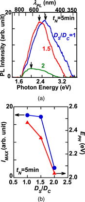
Fig. 14. (Color online) DS /DC- ratio dependence of (a) PL spectrum and (b) IMAX (circles) and EPH (triangles) after N2 annealing (tN = 5 min), where DC is fixed to 4 × 1016 cm−2 and T = 200 °C. Arrows in (a) show EPH-positions. Figure 14(a) shows that the PL spectrum of SiC-QDs strongly depends on DS /DC , that is, DS at a fixed DC . Figure 14(b) shows that the IMAX of SiC-QDs drastically decreases at DS /DC = 2, and in addition, the EPH also decreases with increasing DS /DC .
Download figure:
Standard image High-resolution imageOur previous work 19) showed that the broad PL spectrum of SiC-dots in a-Si can be explained by five PL components of different SiC-polytypes of cubic- and hexagonal-SiC as well as an additional Si–C alloy, whereas the broad PL spectrum of SiC-dots in c-Si is attributable to the sum of only four PL components of different SiC-polytypes, which excludes the Si–C alloy. 21) This Si–C alloy component, which has an EGX < 2.39 eV (3C-SiC), suggests an imperfect SiC structure in SiO2. 19) Actually, Fig. 15(a) shows that the measured PL spectrum at DS /DC = 1 (bold line) can be well fitted via five PL component fitting [Gaussian curve (dashed lines)] even in SiC-QDs, where DC is fixed to 4 × 1016 cm−2, tN = 5 min, and T = 200 °C. Thus, the PL spectrum of SiC-QDs in SiO2 can be also explained by the sum of the PL emissions from four different SiC-polytypes: 3C-SiC, which has an EGX of 2.39 eV (3C: red); 8H-SiC, which has an EGX of 2.73 eV (8H: green); 6H-SiC, which has an EGX of 3.05 eV (6H: blue); 4H-SiC, which has an EGX of 3.32 eV (4H: purple); and an additional one-component of Si–C alloy (SC: brown), which has an EGX of lower than 2 eV. 19) We can estimate the total photon emission number from each PL component, which is an indicator for each polytype ratio for the SiC and Si–C alloy. 19) The integrated PL component ratio PI of the one PL component II to the total IPL emission (subscript I is from SC to 4H), as shown in Fig. 15(a), was calculated using Eq. (6). 19)

where E is the photon energy. Figure 15(b) shows the integrated intensity ratio of the five PL components 19) of SiC-QDs as a function of DS /DC , and the PI ratio strongly depends on DS /DC . The 3C-SiC PL component ratio of approximately 44% is nearly independent of DS /DC . However, with decreasing DS /DC , the hexagonal-SiC PL component ratio increases, and the SC component rapidly decreases. Thus, the SC component indicates that the imperfect SiC formation of the Si–C alloy in SiO2 increases with increasing DS /DC . Consequently, even at the same DC , the SiC-QD formation is strongly affected by DS , and the H-SiC polytype ratio increases with an increasing DC ratio. These results regarding the DS /DC dependence of PL components can indicate that the peak-λPL (EPH) can also be controlled by DS /DC , as shown in Figs. 14(b) and 15(b).

Fig. 15. (Color online) (a) Five PL component fittings [Gaussian curve (dashed lines)] for measured PL spectrum at DS /DC = 1 (solid line) and (b) integrated PL intensity ratios of five PL components of SiC-QD calculated by Eq. (6) as a function of DS /DC , where DC is fixed at 4 × 1016 cm−2, tN = 5 min, and T = 200 °C. Figure 15(a) shows that the PL spectrum of SiC-QDs can also be explained by the sum of five PL components 19) from four different SiC-polytypes of 3C-SiC with EGX of 2.39 eV (I3C: red), 8H-SiC with EGX of 2.73 eV (I8H: green), 6H-SiC with EGX of 3.05 eV (I6H: blue), 4H-SiC with EGX of 3.32 eV (I4H: purple), and an additional one-component of Si–C alloy ISC (brown) with lower EG of 2 eV. Figure 15(b) shows that five PL component ratio of Eq. (6) strongly depends on DS /DC . Hexagonal PL component ratio increases with decreasing DS /DC , but the 3C-SiC PL component is almost independent of DS /DC .
Download figure:
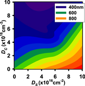
Standard image High-resolution imageAccording to the different PL peak wavelengths versus the type of IV-QDs shown in Figs. 9, 11(b), 12(a), and 14(b), the peak-λPL of IV-QDs in SiO2 can be controlled by the combination of DS and DC . Figure 16 shows the peak-λPL contour map of IV-QDs in various DS and DC conditions obtained from the data in Figs. 9, 12(a), 14(b), and 15(b). A longer λPL can be obtained by increasing the DS at a lower DC . In contrast, a shorter λPL can be realized by increasing the DC at a lower DS . Consequently, the peak-λPL of IV-QDs from near-UV to near-IR regions can be easily designed only by the combination of DS and DC conditions.
Fig. 16. (Color online) Peak-λPL contour map in various DS and DC conditions for designing peak emission wavelength of IV-QDs. This contour map of peak-λPL was obtained using the data from Figs. 9, 12, and 14. A longer λPL can be obtained by increasing DS at a lower DC . In contrast, a shorter λPL can be realized by increasing DC at a lower DS .
Download figure:
Standard image High-resolution image
4. Conclusion
In this work, we experimentally studied the group-IV semiconductor-QDs of Si, SiC, and C in a SiO2 layer fabricated by hot-ion implantation at T and post N2 annealing at a TN of 1000 °C. Si- and C-QDs, in addition to SiC-QDs, can be successfully formed around the middle of the SiO2 layer with a relatively higher dopant concentration using HAADF-STEM. CSTEM also shows clear lattice spots in some areas of IV-QDs, as confirmed by HAADF-STEM, which indicates that some areas of IV-QDs are crystallized. The IV-QD diameter Φ varied from approximately 2–4 nm, and the statistical distribution of Φ can be explained by the Gaussian function. The QD surface-density N was approximately 2 × 1012 cm−2. The Φ and N of the SiC-QDs were affected by T.
The UV-Raman data for the Si- and C-QDs show that the QD crystal quality was improved after N2 annealing because the c-Si Raman intensity of the Si-QDs and the G-band intensity of the C-QDs increased. Moreover, the UV-Raman spectra of the SiC-QDs strongly depend on DS /DC , and the Raman intensities of the TO and D-bands increase with decreasing DS even at a fixed DC , which suggests that the SiC and graphite formations in SiC-QDs increase at low DS conditions.
We experimentally demonstrated strong PL emissions in a wide range of EPH (peak-λPL) values, even from Si- and C-QDs, in addition to SiC-QDs. The PL spectrum line shape strongly depends on the type of IV-QDs, and different EPH (peak-λPL) values can be obtained from 1.56 eV (800 nm) of Si-QDs to 3.3 eV (380 nm) of C-QDs, simply by changing the type of IV-QDs. Moreover, the PL intensity of the IV-QDs drastically increased after a short N2 annealing, which indicates that post N2 annealing is a key process for realizing strong PL intensity by improving the crystal quality of the IV-QDs. The PL intensity of the SiC-dots in the Si layer gradually decreased after a long N2 annealing, which could be attributable to the decomposition of the Si−C bond during long high-temperature annealing. However, the PL intensity of the IV-QDs in SiO2 layer continues to increase with increasing tN , which is advantageous for the thermal stability of IV-QDs. We experimentally confirmed that the PL emission efficiency of Si-QDs is equal to that of SiC-QDs, but the PL emission efficiency of C-QDs was approximately 1/4 that of Si- and SiC-QDs. In addition, for Si-QDs with an average Φ of 2.4 nm, the EPH of 1.56 eV can be explained by the quantum EG -expansion via the Φ reduction. In addition, the HWTM of the PL spectrum of Si-QDs is also attributable to the Si-QD Φ variation effect on quantum EG -expansion in this study. It was also found that the IPL and EPH of Si- and C-QDs depend on the ion doses.
The PL spectrum of SiC-QDs also depends on the DS /DC eve at a fixed DC , and the IPL and EPH increase with decreasing DS /DC . These results suggest that the optimum DS /DC condition exists to realize higher PL intensity and to design a desired EPH (peak-λPL). Moreover, the PL spectrum of SiC-QDs can be also explained by five PL components of different cubic/hexagonal SiC-polytypes and Si–C alloys. With increasing DS /DC , the PL component of 3C-SiC is almost constant, but the hexagonal-SiC component decreases.
Consequently, this work showed that the peak-λPL of IV-QDs can be controlled using only two parameters, DS and DC . A longer λPL can be obtained by increasing DS at a lower DC , and a shorter λPL can be realized by increasing the DC at a lower DS .
In summary, we demonstrated very strong PL emissions from IV-QDs with different λPL values for near-IR in Si-QDs, the visible range in SiC-QDs, and near-UV in C-QDs, showing that it is easy to design a desired peak-λPL simply by controlling the combination of ion doses of Si+ and C+ that are implanted into the SiO2 layer.
Acknowledgments
This work was partially supported by a Grant-in-Aid for Scientific Research from the Japan Society for the Promotion of Science (17K06359).