

Abstract
Here, a microplasma channel was investigated. The design was developed from a recently presented modular microplasma array. The setup consists of three stacked layers: a magnet, a dielectric foil and two nickel foils that are separated by a 120 μm wide gap. The magnet is grounded while the two nickel foils are powered. The channel is in two dimensions identical (50 μm high and 120 μm wide) to a single cavity of the microplasma arrays while it is two orders of magnitude longer. Unlike the microplasma arrays, the channel provides an additional optical access to the inside of the cavity from the side. The setup was operated with a triangular voltage with a frequency of 10 kHz and an amplitude of up to 700 V at atmospheric pressure. Phase resolved emission images were used to investigate the microplasma channel dynamics with line of sight from the top and from the side to the inside of the cavity. The top view images revealed that the discharge in the microplasma channel and the microplasma arrays behave similar. The already known asymmetric discharge behavior, the self-pulsing and the wavelike ignition was also observed in the microplasma channel. For the wavelike ignition in the channel a simple one dimensional model was proposed. With the additional side view images the asymmetric discharge behavior was examined more thoroughly. Unlike in the microplasma arrays, the discharge expands here in both half periods of the applied voltage above the upper edge of the powered electrodes. The discharge extends over a larger width in the half period, in which the potential of the upper electrodes is increasing, while it extends over a larger height in the other half period. Phase resolved images were also used to investigate the ignition phase of the discharge. The discharge ignites in the two half periods on a different height. This was explained by modeling the drift and diffusion of the charged particles between two discharge pulses. The new insights into the discharge dynamics in the microplasma channel will help to understand the behavior of the discharge in the microplasma arrays.
Export citation and abstract BibTeX RIS
1. Introduction
Atmospheric-pressure plasmas can be used for many different technical and biomedical applications. They can be used, for example, for cleaning of exhaust gas, as UV light source, for surface treatment, for killing of bacteria, for depositing thin films or as a detector for hazardous gases [1–3]. Technical plasmas are often constrained in at least one dimension to 10 μm up to a few millimeters. These plasmas are known as microplasmas. No vacuum system is needed to generate these plasmas. Therefore, they can be easily integrated into a production line. It is possible to treat large surfaces or gas flows by the parallel operation of many identical microplasmas. Such microplasma arrays are under investigation for a long time [4, 5].
Microplasma arrays exist in many different configurations. This paper focuses on microplasma arrays that were developed from the inverted pyramid microplasma arrays by the group of Eden [6]. Hereafter, microplasma arrays developed from these designs are simply referred to as microplasma arrays. These microplasma arrays are a special type of dielectric barrier discharges (DBD). The simplest design of a DBD consists of two parallel electrodes that are separated by at least one dielectric layer. This dielectric prevents a current flow between the two electrodes. Therefore, an AC voltage is needed to operate a DBD. DBDs can ignite in two different discharge modes. In the first mode, the discharge ignites in many small discharge filaments. In the second mode, the discharge ignites as one diffuse homogenous discharge. These two modes are induced by different breakdown mechanisms [7–9].
Many species that are not part of the gas feed are produced in a DBD. These include, for instance, electrons, ions, surface charges on top of the dielectric and excited atoms and molecules. Depending on their lifetime, a part of these species is still present when the next discharge is ignited. Thus each discharge is influenced by the preceding discharge [8, 9]. This interaction between the individual discharge pulses is summarized under the term memory effect and is characteristic for DBDs [8]. The memory effect can lead to a transition between a filamentary DBD in the first excitation periods (first two or three) to a homogenous DBD in the following excitation periods [9].
In microplasma arrays many discharges are operated in parallel. Each discharge is ignited in a separate cavity. These cavities are evenly distributed over a surface. The dimensions of the cavities are in the order of 100 μm. Throughout the literature, these microplasma arrays exist based on numerous different materials like silicon [5, 6, 10, 11], ceramics [12] and nickel [13]. The geometry of the cavities also varies throughout the literature. For example, cylindrical [14, 15] and inverse pyramidal [6, 11] cavities were used. Recently, a new modular constructed metal-grid array was introduced which has several advantages [13]. This array consists of a stack of a magnet, a dielectric sheet and a nickel grid. The magnet serves as the grounded electrode and the nickel grid as the powered electrode. The nickel grid contains the cylindrical cavities. Since nickel is ferromagnetic, the magnet pulls down the nickel foil. As a result, the distance between the two electrodes is uniform over the whole surface of the magnet and inhomogeneities in the electric field are reduced. That helps to ignite all cavities of the array. These metal-grid arrays can easily be assembled. They can be disassembled to investigate changes of the surfaces. It is easy to change the material of the dielectric and they have shown resistance against self-destruction for months.
Despite the wide range of used materials and geometries, all microplasma arrays behave similar. One characteristic feature of the microplasma arrays is that the emission structure is different in the two half periods of the applied voltage. The emitting area is smaller than the topside of the cavity in one half period. In the other half period, the discharge emits light mainly from the edges of the cavity. These differences are caused by the different direction of the electric field. The electrons get accelerated into the center and to the bottom of the cavity in one half period. Therefore, the excitation takes place mainly inside the cavity and the emitting area is smaller then the topside of the cavity. In the other half period, the electrons get accelerated to the side walls of the cavity and to the top. In this half period, the excitation takes place mainly at the edges of the cavity [16, 17].
Until now, this explanation for the different emission structure in the two half periods was not yet confirmed. Optical access to the inside of the cavity could provide additional evidence for the above-mentioned explanation of the different emission structure in the two half periods. Additionally, it could give new insights into the electron dynamics. This optical access was for example provided by micro prisms for microplasma arrays used in plasma display panels [18]. Unfortunately the geometry of the plasma display panel arrays is quite different. This makes a comparison to the microplasma arrays developed from the inverted pyramid microplasma arrays difficult. To our knowledge, most of the microplasma arrays with a similar geometry provide optical access to the inside of the cavities only from the top. The optical access from the side is always blocked by the upper electrode.
The setup of the above-mentioned modular constructed metal-grid array was modified to a microplasma channel (compare figure 1) to get this optical access. For this purpose, the upper nickel grid was removed and replaced by two separate nickel foils which are separated by a 120 μm wide gap. This channel now has a similar height and width as one cavity of the modular constructed metal-grid arrays. In the third dimension the channel is about two orders of magnitude longer. The channel is open at the sides which gives the desired optical access.

Figure 1. (a) Sketch of the recently introduced modular metal-grid array [13]. (b) Sketch of the investigated microplasma channel. For both setups the magnet is grounded and a triangular voltage is supplied to the upper nickel electrodes.
Download figure:
Standard image High-resolution imageThis microplasma channel was investigated and compared to the microplasma arrays by phase resolved emission imaging with line of sight from the top into the cavity, in this work. A silicon based microplasma channel was already investigated in the past. Here the optical access to the inside of the cavity from the side was also blocked by the upper electrode. The behavior of the discharge in this channel and a single cavity of the microplasma arrays was very similar [19]. Therefore, it was expected that the discharge in the microplasma channel that was investigated in this work also behaves similar. It was investigated in this work which mechanism could be responsible for the propagation of the discharge along the length of the microplasma channel. The optical access from the side into the microplasma channel was utilized to investigate the different behavior of the discharge in the two half periods that is already known from the microplasma arrays. Additionally, the ignition of the discharge was investigated with phase resolved images with line of sight from the side into the microplasma channel. COMSOL Multiphysics 5.5 was used to calculate the electric field in the microplasma channel and to simulate the drift and diffusion of ions and electrons between two discharge pulses. This simulation was used to explain the dynamics of the discharge during the ignition.
2. Experiment
2.1. Metal-grid arrays
The setup used in this work is based on the metal-grid arrays developed by Dzikowski et al [13]. These arrays consist of a magnet, a dielectric foil and a metal grid. A cobalt–samarium magnet serves as grounded electrode. This magnet was glued into a polyether ether ketone (PEEK) frame. The top of the magnet was polished to reduce inhomogeneities in the electric field due to a variation of the distance between the two electrodes after the magnet was glued into the frame. A 50 μm thick dielectric foil (zirconium oxide,  r ≈ 27) was placed on top of the magnet. The powered electrode is a 50 μm thick nickel foil. A grid of cylindrical cavities was cut into this foil with a laser. The cavities have a diameter in the order of magnitude of 100 μm. The distance between two cavities is in the same order of magnitude. The powered electrode was placed on top of the dielectric foil. The array is operated at atmospheric pressure. Therefore, the mean free path is so small that the influence of the static magnetic field on the plasma is negligible [13]. The top surface of the magnet is 50 mm long and 15 mm wide. The dielectric foil and the nickel foil are a bit larger. They are both 63 mm long and 21 mm wide. This prevents discharges at the edges of the two electrodes. Furthermore this allows to contact both electrodes from the bottom. Thus the optical access is not restricted. A quartz cover (suprasil S1) forms together with the PEEK frame and the magnet an air tight volume of about 2 mm height with the dielectric foil and the nickel grid inside. The gas inlet and outlet is integrated into the bottom of the PEEK frame in such a way that the gas flows across the longer dimension of the magnet.
2.2. Microplasma channel
As for all microplasma arrays of similar geometry, the inside of the cavities of the metal-grid arrays is only accessible from the top for optical measurements. Therefore, the setup was modified. Figure 2(a) shows a schematic sketch of the used setup. The PEEK frame and the quartz cover are not included in this sketch. Additionally, figure 2(b) shows a picture of the microplasma channel device operated in helium. The powered grid electrode was replaced by two separate 50 μm thick nickel foils compared to the metal-grid arrays. These foils were separated by a 120 μm wide gap across the whole width of the dielectric foil. The distance between the two upper nickel electrodes was checked with a laser scanning microscope (Keyence VK-9710) over the full length of the channel after assembling the microplasma channel. The distance between the two upper nickel electrodes varies along the length of the channel by only 0.3 μm per mm. This channel has in two dimensions a similar size as a single cavity of the metal-grid arrays. In the third dimension, the channel is two orders of magnitude larger. The inside of the channel can be accessed from the top and from the side by optical measurements. The rest of the setup is identical to the setup of the metal-grid arrays.

Figure 2. (a) Sketch of the modular microplasma channel device. The quartz cover and the PEEK frame are not included. (b) Picture of the modular microplasma channel device.
Download figure:
Standard image High-resolution imageAll presented measurements were performed multiple times and with different microplasma channels with similar gap width. With the microplasma arrays it was observed that even microplasma arrays with the same geometry behave a little bit different for repetitive measurements due to probably small changes in cleanness or electrical contact. Therefore, one setup including multiple different arrays is needed to investigate parameter dependencies reproducibly. This was for example done by including four arrays with different geometries on a single chip for the silicon based microplasma arrays [20]. It is not possible to create a similar setup without restricting the optical access for the microplasma channel. Therefore, only one geometry of the channel was used. Only the results obtained with one microplasma channel are presented for consistency reasons. However the observed phenomena were similar with the other setups while the absolute values varied slightly. Some results obtained with a different microplasma channel can be found in the appendix
2.3. Diagnostic setup
The gas flow was set by a mass flow controller (Analyt MTC 35831 (0–2 slm)) to 0.5 slm helium (5.0 purity). A cold trap filled with dry ice was used and the microplasma channel device was heated with a dryer prior to every measurement to 50 °C for 20 min to reduce impurities. A function generator (Tektronix AFG3251) and an amplifier (Trek PZD700A M/S) generated a triangular voltage with a frequency of 10 kHz and an amplitude of up to 700 V. This voltage was supplied to both nickel foils. A triangular voltage was used to get results that are comparable to previous experiments and to get a constant derivative of the voltage with respect to the time. This simplifies the analysis. The voltage and current was monitored with an oscilloscope (Tektronix TDS 2014B) with a capacitive voltage probe (Tektronix P6015A) and an inductive current probe (Tektronix P6021) (see figure 2(a)).
Figure 3 shows the optical setup. Two ICCD cameras (Andor iStar DH334T-18U-73 and Andor iStar DH334T-18U-E3) were used to take phase resolved images of the discharge. These two cameras only differ in the type of the photocathode. Phase resolved images are an alternative to time resolved images when investigating low intensity emission of repetitive phenomena with high temporal resolution. Here the trigger signal of the function generator was used to gate the intensifier of the ICCD camera. The gate width can be as low as 2 ns for the used cameras. The CCD chip is exposed once per period of the applied voltage with a constant delay to the transition from negative to positive applied voltage. The CCD is read out after multiple exposures. The resulting image represents a short phase of the applied voltage integrated over multiple periods. The images were taken with line of sight from the top (top view images) and from the side (side view images) into the channel. Two different camera lenses were used (Nikon AF Micro-Nikkor 200 mm 1:4D IF-ED, focal length 200 mm, aperture between f/4 and f/32 and Ricoh FL-BC7838-VGUV, focal length 78 mm, aperture between f/3.8 and f/16). An additional lens (f = 20 mm) was used to get a higher spatial resolution for the side view images and for top view images of sections of the channel. This lens was not used for top view images of the whole channel.

Figure 3. Sketch of the optical setup for phase resolved imaging.
Download figure:
Standard image High-resolution image2.4. Electric field strength
The electric field generated by the applied voltage without any space charges was calculated with COMSOL Multiphysics 5.5. Variations of the electric field along the length of the channel are expected to be small and only caused by inhomogeneities from the production and boundary effects. Therefore, it is sufficient to calculate the electric field in a two dimensional space. COMSOL Multiphysics 5.5 was used to numerically solve Poisson's equation in the dielectric and in and above the cavity with the finite element method with a direct solver. The equation was solved in a space extending 500 μm from the middle of the channel in both directions and 500 μm above the upper electrodes. This space was meshed using a triangular mesh with element sizes between 0.03 μm and 10 μm. A finer mesh was used within the cavity (minimum mesh size: 0.03 μm, maximum mesh size: 0.1 μm) while the mesh in the dielectric and above the cavity was coarser (minimum mesh size: 0.3 μm, maximum mesh size: 10 μm). The maximum element growth rate was set to 1.1, the curvature factor to 0.3 and the resolution of narrow regions to 1 in the whole space. The inside of the cavity was meshed first and the rest of the space afterward. The potential was set to zero on the lower edge of the dielectric while it was set to the applied voltage on all edges of the upper electrodes as a boundary condition. The surface charge density was set to zero on all other outer boundaries.
Figure 4 shows the magnitude of the electric field on a logarithmic color coded scale for an applied voltage of 200 V. This voltage is needed to ignite the discharge (compare section 3.2.2). The two nickel electrodes are illustrated in gray. Additionally, the black arrows show the direction of the electric field. The length of the arrows is proportional to the electric field strength at the starting point of the arrows. The direction of the electric field strength and its distribution depend only on the geometry and the sign of the applied voltage. The magnitude of the electric field strength is proportional to the applied voltage. Therefore, it is possible to calculate the electric field strength for any other applied voltage from figure 4. The highest electric field is in the bottom corners of the microplasma channel. The electric field strength decreases to the middle of the channel. From the bottom of the channel to the top, the electric field strength decreases as well. Inside the microplasma channel the electric field points from the nickel electrodes to the middle of the channel and to the surface of the dielectric foil.
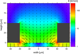
Figure 4. Color coded map of the electric field strength in the channel induced by the applied voltage. Calculated with COMSOL Multiphysics 5.5 without any space charges. The two nickel electrodes are illustrated in gray. The arrows show the direction of the electric field. The length of the arrows is proportional to the electric field strength at the starting point of the arrows.
Download figure:
Standard image High-resolution imageThe electric field strength changes inside of the cavity and especially in the bottom corners quite drastically. Therefore, not only the maximum value of the electric field strength determines whether a discharge is ignited but also the size of the area where the electric field strength is higher than a needed threshold. The electrons gain energy from the electric field over the characteristic length of their mean free path. The mean free path of electrons (λe) in helium can be calculated from the gas density (ngas) and the effective collision cross section (σ):

kB is here the Boltzmann constant, Tgas the gas temperature and p the pressure. For an assumed electron energy between 1 eV and 10 eV (compare [21]) the effective collision cross section of electrons and helium atoms is between σe = 7 × 10⁻²⁰ m2 and σe = 4.7 × 10⁻²⁰ m2 [22]. The calculated electric field strength was averaged over circles with the mean free path of the electrons as diameter. This yields a maximum value of 255 kV cm−1 (10 eV electrons) to 312 kV cm−1 (1 eV electrons). Multiplying these values with the mean free path of the electrons and the elementary charge yields an energy between 18 eV and 22 eV.
The different geometry of the microplasma arrays results in a different spatial electric field configuration. In the microplasma channel the cavity is confined only along the width by an electrode. In the microplasma arrays the cavity is also confined along the length by an electrode. These additional confinement provides an additional contribution to the electric field.
3. Results and discussion
3.1. Top view images
3.1.1. Self-pulsing
Figure 5 shows the intensity emitted by the discharge in the microplasma channel and the applied voltage in dependence of the time during one cycle of the applied voltage. The intensity was measured with top view images with the ICCD camera. The additional 20 mm lens was not used for this measurement. Therefore, the whole microplasma channel was investigated. The measured intensity was then integrated over the whole microplasma channel. The images were taken at a frequency of 10 kHz and an amplitude of 650 V for the applied voltage. The gate width of the ICCD camera was set to 200 ns and the exposure time was set to 0.017 s. This means that each image is a phase resolved average over 170 excitation cycles.

Figure 5. Temporal total light intensity development (black line) compared to applied voltage (red line). The intensity is measured by integrating over phase resolved camera images of the whole microplasma channel.
Download figure:
Standard image High-resolution imageFigure 5 shows that the discharge is ignited two times per excitation cycle and emits light. The emitted intensity pulses with a frequency of about 300 kHz during these two discharge phases (tdelay = −9 μs to tdelay = 27 μs and tdelay = 40 μs to tdelay = 77 μs). This pulsing is typical for a DBD [8, 23–26] and is also known from the microplasma arrays [16, 17]. The discharge is ignited as soon as the electric field strength is high enough. High enough means in this context again the combination of exceeding a needed threshold in an area and the size of that area, as already described in section 2.4. A conducting discharge channel is formed between the dielectric and the upper electrode after the ignition. A current flows through this channel. Surface charges are accumulated on top of the dielectric, as a result. These surface charges reduce the electric field strength until the field can no longer sustain the discharge. Since the applied voltage is still increasing, a new discharge is ignited as soon as the electric field strength is again high enough yielding another emission pulse. This pulsing continues until the slope of the applied voltage is reversed. The reduction of the electric field strength by the surfaces charges is no longer compensated by the increasing applied voltage at this point [8, 24, 27, 28].
The direction of the electric field strength is different in both discharge phases. Therefore, the electrons and ions get accelerated in different directions. In the first discharge phase (tdelay = −9 μs to tdelay = 27 μs), the ions get accelerated to the top of the dielectric and adsorb there as surface charges. The electrons get accelerated to the upper electrodes and recombine there in this discharge phase. In the other discharge phase (tdelay = 40 μs to tdelay = 77 μs), the electrons get accelerated to the top of the dielectric and adsorb there as surface charges while the ions get accelerated to the upper electrodes where they recombine. Since the ions are much heavier, their mobility is much lower than the mobility of the electrons. The mobility of the ions is still high enough that they reach the top of the dielectric in less than 0.5 μs in the first discharge phase as will be shown later. This is still an order of magnitude lower than the period length of the self-pulsing. Therefore, the electric field strength gets in both discharge phases shielded very quickly by the surface charges as soon as the field strength is high enough to ignite a discharge. This shielding causes the discharge to end. Now the applied voltage has to rise again to ignite the next discharge pulse. The time until the voltage has risen enough is due to the triangular voltage the same in both discharge phases. Therefore, the frequency of the self-pulsing is identical in both discharge phases.
The amplitude of the individual pulses decreases and a continuous emission is building up during both discharge phases as can be seen in figure 5. This indicates that the mode of the discharge is changing from a mode with a high current density to one with a lower current density. A lot of surface charges accumulate on top of the dielectric in the high current mode. These surface charges shield the electric field which leads to the self-pulsing of the discharge. The accumulation of surface charges is slower in a lower current mode. Therefore, the shielding for the electric field is smaller and faster compensated by the increasing applied voltage. This ultimately leads to a smaller amplitude of the self-pulsing and instead to a more continuous emission.
DBDs can ignite in a filamentary or a diffuse homogeneous discharge mode. In the filamentary mode, many small microdischarge channels (radius about 100 μm) are ignited as soon as the applied voltage is high enough. These channels are generated in a streamer breakdown [29, 30]. In the homogenous mode, the discharge ignites in a Townsend breakdown with secondary electron emission at the cathode and electron impact ionization in the gas volume between the electrodes. To achieve this mode, a streamer breakdown has to be suppressed. It is important that the ionisation in the volume is slow enough that the ions can reach the cathode before the electric field generated by the space charges is high enough to cause a streamer breakdown [9]. Enhancing the secondary electron emission can also help to achieve a homogenous DBD. Charges that were adsorbed on top of the dielectric in the preceding discharge pulse have a lower binding energy to the surface than the intrinsic electrons of the dielectric. Therefore, they enhance the secondary electron emission coefficient and favor a homogenous DBD [9]. A sufficiently high preionization in the volume can also favor a homogenous DBD. The preionization causes an overlap of the ionisation avalanches. Thus transverse gradients of the charge density get reduced and the formation of a streamer gets suppressed. This preionization can be left over from previous discharge pulses [8]. Additionally, ions that are left over in the volume from previous discharge pulses can contribute decisively to the emission of secondary electrons during the ignition [9]. The amplitude and shape of the applied voltage can also cause a transition between the filamentary and the homogenous mode. A higher amplitude or slew rate can cause a transition from a homogenous DBD to a filamentary one [28, 31]. A higher degree of impurities in the feed gas can also cause the transition to a filamentary DBD [31]. In the filamentary mode the current density is 3–20 times higher than in the diffuse homogenous mode [8].
A transition between these two discharge modes could be responsible for the decreasing amplitude of the individual pulses and the transition to a more continuous emission during one discharge phase. At the beginning of both discharge phases, there are only a few free charges left over from the previous discharge phase in the volume of the channel. A streamer is ignited as soon as the electric field strength is high enough. The current flowing through the streamer channel leads to an accumulation of charges on the surface of the dielectric and thus to a reduction of the electric field strength until the discharge can no longer sustain it self. The next discharge pulse follows after about 1.8 μs. This temporal distance is one order of magnitude lower than the temporal distance between the two emission phases (15.0 μs). Consequently, there are more free charges in the volume that are left over from the previous discharge pulse at the beginning of the later pulses of one discharge phase than at the beginning of the first pulse of a discharge phase. This higher preionisation favors the Townsend like DBD mode. Therefore, the following discharge pulses in the same discharge phase behave more like a Townsend discharge with a lower current density. This lower current density leads to a slower accumulation of charges on the surface of the dielectric. Accordingly, the reduction of the electric field can be partially compensated by the increasing applied voltage. This leads to a lower amplitude of the pulsing of the emission and instead to a more continuous emission. A transition between the two discharge modes was already observed for DBDs. The discharge first ignited in the filamentary mode and transitioned after one excitation period to the homogenous mode [9].
3.1.2. Asymmetric discharge behavior
The discharge in the microplasma arrays behaves different during the two emission phases. The discharge in the microplasma channel shows a similar behavior as will be shown later. In the literature, the polarity of the applied voltage is often used to define two half periods (positive half period PHP and negative half period NHP) and to compare the different behavior of the discharge during both half periods. The reason for the different behavior of the discharge during the two discharge phases is the different direction of the electric field. As for all DBDs, there is a contribution of the applied voltage (Evoltage) and the surface charges (Esc) on top of the dielectric to the electric field [8, 27]. The polarity of the applied voltage is a good criterion to define the two half periods as long as the contribution of the surface charges is low. Figure 5 shows that the discharge ignites for the used operation conditions for both discharge phases before the applied voltage changes its sign. The reason is that for the used conditions the surface charges create an electric field strength that is high enough to ignite a discharge. For example at the end of the discharge phase from tdelay = 40 μs to tdelay = 77 μs, the upper electrode was on a negative potential. Therefore, the electrons were accelerated to the dielectric and accumulated on top of it as surface charges. As soon as the slope of the applied voltage changes from negative to positive, the shielding of the electric field by the surface charges gets no longer compensated by the increasing applied voltage. Thus, the electric field strength (Esc + Evoltage) is no longer high enough to sustain the discharge. The contribution of the applied voltage to the electric field decreases now until the voltage changes its sign. The surface charges create an electric field in the opposite direction which is alone strong enough to ignite a new discharge. As soon as the electric field created by the applied voltage has decreased enough (at tdelay = −9 μs), a new discharge is ignited by Esc. The electric field is now pointing in the opposite direction compared to the end of the previous discharge phase. Now positive ions are accelerated to the dielectric. The electrons on the surface are getting neutralized and afterward positive ions are accumulated as surface charges. These ions generate the electric field that causes the ignition in the following emission phase (at tdelay = 40 μs). This behavior is already known from parallel plate DBDs [28].
The polarity of the applied voltage is no longer a good criterion to define the two half periods since the contribution of the surface charges to the electric field is no longer small compared to the contribution of the applied voltage to the electric field under these conditions. The slope of the voltage is instead a much better criterion to define the two half periods since the discharge always ends as soon as the slope of the voltage is reversed. In the following the half period where the potential of the upper electrode is increasing is called 'increasing potential phase' (IPP). The slope of the voltage is here positive. The half period where the potential of the upper electrode is decreasing is called 'decreasing potential phase' (DPP). The slope of the voltage is here negative.
Figure 6 shows the intensity of the light emitted by the discharge from a 2.2 mm long section of the channel averaged over the IPP (figure 6(a)) and DPP (figure 6(b)) respectively for top view images. The black lines indicate the position of the edges of the channel. The images used for these figures were taken with the additional 20 mm lens to get a higher spatial resolution. The images were again taken at a frequency of 10 kHz and an amplitude of 650 V for the applied voltage. The area from which the discharge emits light is different for the two half periods. In the IPP the discharge emits preferentially light from two areas close to the edges of the channel. In the DPP the light is emitted from the center of the channel. A similar behavior is already known from microplasma arrays [16, 17]. The differing behavior is caused by the different direction of the electric field. In the IPP, the electrons are accelerated to the edges of the channel and away from the dielectric. In the DPP, the electrons are accelerated in the opposite direction to the center of the channel and to the dielectric (compare figure 4). This results in the observed spatial distribution of the emission.

Figure 6. Top view images of the discharge emission from a 2.2 mm long section of the channel averaged over (a) the IPP and (b) DPP. The black lines indicate the edges of the channel. The intensity is for both images normalized to the maximal emission in the IPP.
Download figure:
Standard image High-resolution image3.1.3. Wavelike ignition
Another characteristic feature of the microplasma arrays is the wavelike ignition. The individual cavities are usually not ignited simultaneously. Instead the discharge ignites in one or a few cavities first. From these cavities the discharge expands across the remaining cavities in a wave like pattern. The wave travels across the array with a velocity in the km s−1 range [13, 16, 32]. In the earlier mentioned silicon based microplasma channel these waves were also observed with similar velocities [19]. Presumably because of irregularities from the production of the microplasma array the electric field strength is a bit higher in some cavities. Therefore, the discharge ignites at first in these cavities [13, 32]. From here, the discharge propagates over the rest of the microplasma array. Until now, the driving mechanism for this propagation has not been fully understood yet. A simulation by Wollny et al [33] for a silicon based microplasma array with pyramidal cavities indicated that the propagation is driven by the drift of electrons followed by the drift of ions between the cavities initiated by photoemission of electrons. Without the emission of photoelectrons the propagation velocity in the simulation was half an order of magnitude lower than the experimentally observed velocity. However this simulation only treated the propagation for the case that the upper electrode is negatively biased.
To investigate if the microplasma channel shows a similar behavior, the 20 mm lens was removed. This reduces the spatial resolution so far that the microplasma channel could be imaged over the full length at once. Again phase resolved images were taken with this setup at a frequency of 10 kHz and an amplitude of 650 V for the applied voltage. The gate width of the ICCD camera was set to 200 ns and the exposure time to 17 ms. The measured intensity was then integrated over the width of the microplasma channel for each image. The variation of the emitted intensity is visualized both in time and position along the length of the channel by plotting the position along the length of the channel on the y-axis, the temporal position corresponding to each image on the x-axis and the measured intensity as a color code.
Figure 7 shows this evolution for the IPP and figure 8 for the DPP. The origin of the time axis is the same as in figure 5 (i.e. at tdelay = 0 μs the applied voltage changes from negative to positive). In figure 7 it is obvious that the first ignitions of the discharge in the IPP take place at six locations (marked with white numbers). Hereafter, these discharges are referred to with these numbers. These first ignitions start independent of each other. These ignitions happen within a time interval of 1.6 μs. It can be assumed that the first ignitions take place at these locations since the electric field strength is higher at these positions due to irregularities caused by the production.
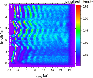
Figure 7. Phase space diagram of the discharge emission from the full channel in the IPP. The white numbers mark the first discharges in this half period. The white arrows indicate the propagation of these first discharges.
Download figure:
Standard image High-resolution image
Figure 8. Phase space diagram of the discharge emission from the full channel in the DPP. The white numbers mark again the first discharges in this half period and the white arrows indicate again the propagation of their.
Download figure:
Standard image High-resolution imageFrom these positions the individual discharges propagate along the channel with velocities between (0.37 ± 0.24) km s−1 and (1.9 ± 0.4) km s−1. The propagation velocity is higher if the distance to the next discharge location is larger. This influence of the distance between the discharges on their propagation velocity is already known from the silicon based microplasma channel [19]. The measured velocities are similar to the velocities measured with the microplasma arrays [13, 16, 32] and the silicon based microplasma channel [19]. The white arrows in figure 7 mark the propagation of the discharges. A steeper arrow indicates a higher propagation velocity. The length of the arrows indicate the propagation distance of the individual discharges.
Comparing figures 7 and 8 it can be observed that besides the amplitude of the emitted intensity the differences between the IPP and the DPP are small. In fact the only other difference is the temporal difference between the ignition of the first discharge pulses. For instance discharge 2 ignites about 1 μs later than discharge 6 in the IPP while it ignites about 0.2 μs earlier in the DPP.
The transition from a pulsing mode to a more continuous mode is again observed in figure 7. The frequency of the pulsing is again about 300 kHz which was already observed with the spatially integrated intensity (compare section 3.1.1). Additionally, it is visible in figure 7 that the discharges that ignite at the beginning of each half period extend over a length of about 100 μm to 600 μm which is quite similar to the diameter of the microdischarge channels observed in the filamentary DBD mode (200 μm to 400 μm [9, 29]). It is clearly visible that the emitted intensity from the first discharge pulses is significantly higher than in the later part of the half period. Additionally, the emitted intensity is for the first discharge pulses concentrated to small areas while it gets more diffuse in the later part of the half period. This indicates that the current density is also higher in the first discharge pulses.
All observations mentioned in the previous paragraph indicate a transition from the filamentary DBD mode which is driven by the streamer mechanism to the homogenous DBD mode with a Townsend ignition.
3.1.4. Propagation velocity
In this section, the measured propagation velocities of the first discharges will be compared to the drift and diffusion velocity of the ions and electrons. With Fick's first law, the diffusion velocity vdiffusion can be calculated:

n is here the particle density, D is the diffusion coefficient and l is the position along the length of the channel. The gradient of the electron density can be estimated from the gradient of the emitted intensity assuming that the excited species are produced mainly by electron collisions and that the gradient of the electron density is much larger than local deviations of the electron energy distribution function. Figure 9 shows the measured intensity in dependence of the position along the length of the channel immediately after the ignition of discharge 1. An exponential fit is used for the decay of the emitted intensity from the maximum intensity to the left. With the previously mentioned assumptions, this fit is used to approximate the gradient of the electron density:


I is here the measured intensity and I0 is a constant. The electron diffusion coefficient can be calculated from the Boltzmann constant (kB), the gas temperature (Tgas), the electron mass (me) and the mean collision frequency (νm):


Figure 9. Normalized intensity integrated over the channel width around position 1 (compare figure 7). The red line shows a fit of an assumed electron density generating the emission.
Download figure:
Standard image High-resolution imageThe mean collision frequency can be calculated from the gas density ngas, the effective collision cross section (σ) and the mean velocity ( ):
):

For an assumed electron energy between 1 eV and 10 eV (compare [21]), the effective collision cross section of electrons and helium atoms is between σe = 7 × 10⁻²⁰ m2 and σe = 4.7 × 10⁻²⁰ m2 [22]. The mean electron velocity can be calculated for a Maxwell–Boltzmann velocity distribution. For a gas temperature of 300 K and atmospheric pressure, this leads to a diffusion coefficient for the electrons smaller (or equal) than De = 3.4 × 10⁻³ m2 s−1. The effective collision cross section for helium ions and helium atoms at an ion and gas temperature of 300 K is σI = 1 × 10⁻¹⁸ m2 [34]. This yields a diffusion coefficient for the ions of DI = 2.0 × 10⁻⁵ m2 s−1. With equation (2) the diffusion velocity of the electrons and ions results to:


Even the free diffusion of electrons yields a velocity that is about two orders of magnitude lower than the propagation velocity of the discharges. The velocity of the ambipolar diffusion is between the velocity of the free diffusion of the ions and electrons. Therefore, the ambipolar diffusion can also not explain the propagation of the discharge along the length of the channel.
The Einstein relation correlates the mobility (μ) of the electrons and ions with the diffusion coefficients:

e is here the elementary charge. The drift velocity (vdrift) of a charged particle in an electric field (E) is vdrift = μE. This means that an electric field strength of at least 1.4 × 10⁴ V m−1 along the length of the channel is required to achieve a drift velocity of 1.9 km s−1 for the electrons. This field strength would be required over a length of up to 3 mm (compare discharge 1 in figure 7). Additionally, this electric field would have to point in both half periods in the same direction since the propagation is observed in both half periods with the same direction and velocity. For the ions, the electric field strength must be two orders of magnitude higher to achieve the same velocity. To examine if this field strength along the length of the channel would be realistic, COMSOL Multiphysics 5.5 was used to calculate the three-dimensional electric field strength in the microplasma channel. It was tested if a variation of the voltage between the upper electrodes and the magnet along the length of the channel could yield an electric field strength along the length of the channel that is high enough to be responsible for the propagation of the first discharges. Since both electrodes are metallic, this voltage variation is in reality not possible. This test was made to simulate local reductions or enhancements of the electric field strength by surface charges on top of the dielectric. Additionally, it was tested if a variation of the distance between the upper electrodes and the magnet could yield the required field strength along the length of the channel. With both tests it was not possible to achieve the required field along the length of the channel with reasonable values for the voltage variation or the distance variation respectively. Thus, the propagation of the first discharges is also not driven by the drift of electrons or ions.
3.1.5. Propagation model
Since the velocities estimated above do not provide an explanation for the propagation of the discharge, a simple one-dimensional model for the propagation along the length of the channel will be presented in this paragraph. Figure 10 illustrates this model. At one position (L0) the electric field strength is higher due to production inaccuracies (top left graph in figure 10). As the applied voltage increases the electric field strength increases in the whole channel while it remains a bit higher at L0. As soon as the applied voltage is high enough the discharge ignites at position L0 and a current is flowing at this position (top right graph in figure 10). This current leads to an accumulation of surface charges on top of the dielectric at position L0. These surface charges reduce now the electric field strength at position L0 (bottom left graph in figure 10). Now the electric field strength at the wings of the discharge is higher than in the center. Therefore, the maxima of the current density also move from the center of the discharge in both directions (bottom right graph in figure 10).
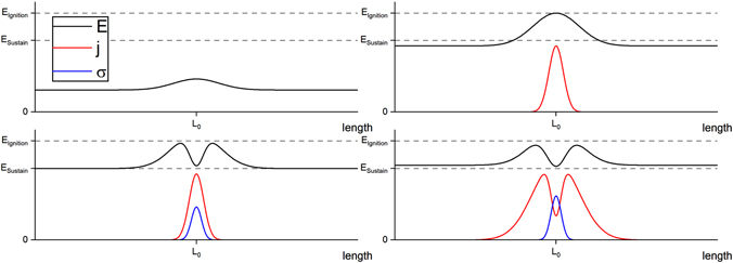
Figure 10. Illustration of the model for the propagation of the discharges along the length of the channel. E is here the electric field strength, j is the current density and σ is the surface charge density. All three are plotted as a function of the position along the length of the channel.
Download figure:
Standard image High-resolution imageFor the ignition of the discharge a higher electric field strength (Eignition) is necessary than for sustaining (Esustain) the already ignited discharge. At the wings of the discharge the electric field strength only needs to sustain the discharge because it was already ignited. The electric field strength necessary for sustaining the discharge is reached with increasing applied voltage earlier than the electric field strength necessary for the ignition of a new discharge. Hence the discharge does not ignite at each location as soon as the field strength at that location overcomes the ignition threshold. Instead the discharge propagates from L0 along the length of the channel. An independent new discharge at a different position L1 only gets ignited, if the electric field strength at L1 passes the ignition threshold earlier than the propagating discharge from L0 reaches L1.
This model can also explain why the propagation velocity is higher if the distance to the next discharge is larger. For the discharges that are close to each other the areas on top of the dielectric where surface charges are accumulated partially overlap. Therefore, it takes longer until the electric field strength at the wings of the discharges gets higher than in the middle.
This model also explains why the discharge travels from all positions only in one direction after the first ignition. For the two discharges at the edges of the channel (1 and 6) the explanation is trivial. These discharges can only travel toward the middle of the channel. The three discharges 3, 4 and 5 are so close to each other that the surface charges created by one discharge also reduce the electric field strength at the locations of the neighboring discharges. This prevents the propagation of the discharge in the middle (4) and the other two discharges can only propagate outwardly. Discharge 2 also propagates only in one direction although the distance to the other discharges is significant larger. This is most likely caused by some inhomogeneities caused by the production which favor one propagation direction. The surface charges created in the first discharge pulse in one half period partially compensate these inhomogeneities. Therefore, discharge 2 propagates from this location in both directions for the following pulses of the same half period.
3.2. Side view images
The top view images showed many similarities between the microplasma channel and the microplasma arrays. There are also a few more similarities between the microplasma channel and the microplasma arrays that are not shown in this paper. For example the current and voltage characteristics and the emission spectra are very similar. Therefore, the geometry of the microplasma channel can now be utilized to get new insights into the discharge dynamics with side view images of the discharge. The next paragraphs present the findings that were gained from these images. These images were all taken with the additional 20 mm lens. The depth of focus is about 100 μm with this lens. The focus point was along the length of the channel close to the end that was closer to the camera (L ≈ 1 mm in figure 7). Since the channel is 15 mm long, only the light emitted from a small section of the channel is imaged acute onto the camera sensor. The light emitted from the rest of the channel is imaged out of focus. Additionally, the solid angle from which light is collected by the optical system is smaller for areas close to the electrodes or the dielectric foil due to vignetting. This must be taken into account when analysing the images.
3.2.1. Emission structure
The two images on the left-hand side of figure 11 show the measured intensity averaged over the IPP (upper image) and the DPP (lower image). The two black meshes indicate the approximate position of the two nickel electrodes and the red mesh indicates the position of the dielectric foil. The images are blurred because of the low depth of focus.
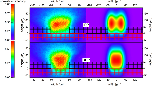
Figure 11. Side view imaging of the emission from the channel in IPP (top row) and DPP (bottom row). The left column shows false color intensity distributions as provided by the ICCD camera. The right column shows respective distributions provided by a simple model. Electrodes and dielectric are indicated by black and red meshes, respectively.
Download figure:
Standard image High-resolution imageNevertheless together with the information from the top view images (figures 6(a) and (b)), it is still possible to recreate a model of the spatial dependency of the emitted intensity. In the top view images the measured intensity is the integral of the emitted intensity over the full height of the discharge. The dependency of the measured intensity on the position along the width of the channel can be fitted quite well by the sum of two Gaussian functions. The ansatz:
for the emitted intensity ((w, h)) recreates the dependency, which was observed in the top view images. w is here the position along the width of the channel, h the position along the height and K, w1, w2, σ1, σ2 and h0 are constants. w1 and w2 are the positions along the width of the channel of the left and right emission maximum (compare figure 6). σ1 and σ2 are the decay distances of the intensity along the width and the height of the channel. h0 is the position of the emission maximum along the height of the channel.
σ1 and the difference between w1 and w2 can be determined from the top view images. The middle of the emitting area observed in the side view images determines then the absolute value of w1 and w2 and h0. σ2 can be determined from σ1 and the ratio of the expansion of the emitting area along the width and the height observed in the side view images.
The images on the right side of figure 11 show the results of this ansatz for the IPP (upper image) and the DPP (lower image). By comparing the images on the right side of figure 11 to the images on the left side it becomes noticeable that the left images look like blurry versions of the images on the right side. Therefore, it can be assumed that the used ansatz probably fits the actual spatial dependency of the emitted intensity quite well.
It is visible that the discharge expands in the IPP over a larger width (about 30% wider) and over a smaller height (about 10% lower) than in the DPP. The upper edge of the discharge is in both half periods approximately on the same height (about 70 μm above the top of the powered electrodes) while the lower edge of the discharge is in the DPP about 15 μm lower than in the IPP. These differences can be explained by the different directions of the electric field. This accelerates the electrons in different directions in the two half periods. In the IPP the electrons are accelerated up and toward the sides of the channel, while they are accelerated down and toward the middle of the channel in the DPP. Thus, the discharge extends over a wider area in the IPP. Since the electric field strength decreases with the distance to the top of the dielectric foil (compare figure 4), the effect of the different direction of the electric field is much stronger for the lower edge of the discharge than for the upper edge. Hence the upper edge is in both half periods on the same height and the lower edge is in the IPP higher than in the DPP.
The expansion along the height of the channel is different to the behavior that was observed with the microplasma arrays. As already mentioned a few times the inside of the cavities of the microplasma arrays is blocked for the side view by the upper electrode. But it is still possible to observe the expansion of the discharge above the upper electrode from the side. These measurements showed that in the microplasma arrays the discharge expands only in the IPP out of the cavity. In the DPP on the other hand the discharge does not expand above the upper electrode [13]. This difference can be caused by the different geometry of the cavities. This different geometry results in a different electric field distribution. The electric field strength for the cylindrical cavity microplasma arrays can be received by rotating figure 4 around the central axis (width = 0). A rectangular area in figure 4 is therefore equivalent to a hollow cylinder in the cylindrical cavity microplasma arrays while it is equivalent to a rectangular cuboid in the microplasma channel. The volume of these hollow cylinders increases with increasing distance to the central axis while the volume of the cuboids stays constant. Thus, the areas further away from the central axis are more important in the microplasma arrays. Inside the cavity the electric field strength increases with the distance to the central axis. Hence the acceleration of the electrons into the cavity in the DPP and out of the cavity in the IPP is stronger in the microplasma arrays. This leads to larger differences of the emission structure in the microplasma arrays between the two half periods.
3.2.2. Drift and diffusion between two discharges
With the side view images, it was also possible to investigate the ignition of the discharge in the microplasma channel. The movement of the electrons and ions between the discharges in the two half periods determines the ion and electron density in the volume right before the ignition. Analysing this movement therefore helps to understand the dynamics of the ignition.
Figure 12 shows the momentary applied voltage during the ignition as a function of the amplitude of the applied voltage waveform for both half periods. The ignition is here arbitrarily defined as the point in time when the emitted intensity reaches 10% of the maximal emitted intensity in the same half period. With increasing amplitude of the applied voltage waveform the momentary applied voltage during the ignition increases in the DPP and decreases in the IPP. This means that with increasing amplitude of the applied voltage waveform the ignition takes place sooner after the slope reversal of the applied voltage in both half periods. This can be explained with the memory effect: at higher amplitudes more surface charges are accumulated on top of the dielectric during one half period. In the next half period these charges enhance the electric field strength. Therefore, a smaller contribution from the applied voltage to the electric field strength is needed to reach the field strength that is physically required to ignite the discharge. At amplitudes higher than about 400 V the surface charges create an electric field strength that is high enough to ignite the next discharge on its own. Only the still applied external field after the slope reversal prevents this. Hence the discharge ignites at these elevated amplitudes before the applied voltage changes its sign.

Figure 12. Applied voltage during the ignition of the first discharge pulse for both half periods as a function of the amplitude of the applied voltage. The ignition is here arbitrarily defined as the point in time when the emitted intensity reaches 10% of the maximal emitted intensity in the same half period.
Download figure:
Standard image High-resolution imageWith the linear fit to the measured voltages displayed in figure 12, it is possible to estimate that at an amplitude of about 200 V the discharge ignites only at the extreme of the applied voltage. This amplitude is at least needed to ignite the discharge in each half period. Below this voltage will be called the ignition voltage (Uignition = 200 V). The contribution of the surface charges and charges in the volume to the electric field is negligible at this amplitude, since the duty cycle of the discharge is so small at this amplitude. It is therefore possible to calculate the electric field strength that is needed to ignite the discharge (compare figure 4).
The slope of the linear fit in figure 12 is close to unity. This means that the applied voltage changes by about 400 V (i.e. twice the ignition voltage) between the extreme values of the applied voltage (i.e. the end of a discharge half period) and the ignition of the subsequent discharge. This also means that the surface charge density stays almost constant between the different discharges in the two half periods. If for example the surface charge density would decrease between the discharge in the two half periods, the applied voltage had to change by more than twice the ignition voltage. This is because the applied voltage would then be responsible to change the direction of the electric field (here a change of 400 V is needed) and to compensate for the decreased surface charge density to ignite the discharge in the next half period. The surface charge density was measured in the past with the electro-optic Pockels effect in parallel plate DBDs. There the surface charge density also remained constant between two discharges [27, 28].
Additionally, the amplitude of the applied voltage has only minor influences on the position and expansion of the discharge (not shown here). In consequence, the spatial distribution of the electric field created by the surface charges needs to be similar to the spatial distribution of the electric field created by the applied voltage. Therefore, the ansatz:

will be used for the sum of the electric field created by the applied voltage ( ) and by the surface charges (
 ) for a first calculation of the movement of the electrons and ions between two discharges. The two different signs are for the time after the discharge in the IPP(+) and after the discharge in the DPP(−). t is here the time after the extreme value of the applied voltage (i.e. after the maximum for the time after the discharge in the IPP and after the minimum for the time after the discharge in the DPP). The electric field created by the applied voltage at a voltage of 200 V (
 (200 V)) was already calculated before (compare section 2.4). Δtoff is here the time between the end of a discharge and the ignition of the discharge in the subsequent half period. For an amplitude of the applied voltage of 650 V Δtoff is about 14 μs. This ansatz means that the electric field strength changes linearly from the electric field strength generated by an applied voltage of ±200 V to the electric field strength generated by an applied voltage of ∓200 V between the end of one discharge and the ignition in the subsequent half period. The upper signs are again for the time after the discharge in the IPP and the lower signs for the time after the discharge in the DPP respectively.
For a low degree of ionisation, the electric field created by the free charges in the volume can be neglected. This is of course an oversimplification of the problem and most certainly not fulfilled at an amplitude of the applied voltage of 650 V. Nevertheless, the results of the following calculations help to understand the dynamics of the ignition. With these simplifications the movement of the electrons and ions caused by drift in the electric field and diffusion can be calculated. The particle flux of the electrons or ions ( ) is:
) is:

With the electron or ion density ne,I, the mobility of the electrons or ions μe,I and the diffusion coefficient of the electrons or ions De,I respectively. Together with the continuity equation this leads to:

This differential equation was solved time resolved with COMSOL Multiphysics 5.5. Assuming that collisions with electrons are responsible for the excitation, the light emitted from each location in the microplasma channel depends on the local electron density and the local electron energy distribution function. Assuming that the spatial gradients of the electron density are large compared to the spatial differences of the electron energy distribution function, the spatially resolved structure of the emitted light (compare figure 11) can be used as the initial condition for the electron and ion density. Variations along the length of the channel are again expected to be small (compare end of both half periods in figures 7 and 8). Therefore, the differential equation was solved in a two dimensional space extending 2 mm from the middle of the channel into both directions and 2 mm above the upper electrodes. As a boundary condition, the ion and electron density right in front of the surfaces of the dielectric and the electrodes is zero since the recombination at the surfaces of the electrodes and the adsorption of ions and electrons reaching the top of the dielectric is assumed to be fast. The distance to the discharge is very large for all other outer boundaries. Hence, the ion and electron density was also set to zero on these boundaries. The electric field was again calculated as in section 2.4 with the larger space above the dielectric. A triangular mesh was used for the calculation of the electric field and the ion and electron densities. The settings for the meshing in the three areas are summarized in table 1. The area of the dielectric was only included and meshed for the calculation of the electric field. The inside of the cavity was meshed first and the remaining area afterward. A backward differentiation formula solver was used to calculate the ion and electron density for each time step. The solver used free time steps with a relative tolerance of 0.001. This means that the solver automatically makes smaller time steps to satisfy this tolerance if necessary.
Table 1. Settings for the meshing of the different areas for the calculation of the ion and electron density. The area of the dielectric was only meshed for the calculation of the electric field. Additionally, the number of elements on the left and right edge of the cavity was set to 2000, on the lower edge to 3000 and on the upper edge to 500. The inside of the cavity was meshed first and the two remaining areas afterward.
| Area | |||
|---|---|---|---|
| Cavity inside | Above the cavity | Dielectric | |
| Minimum mesh size (μm) | 0.02 | 1.2 | 1.2 |
| Maximum mesh size (μm) | 10 | 268 | 268 |
| Maximum element growth rate | 1.05 | 1.1 | 1.2 |
| Curvature factor | 0.3 | 0.3 | 0.3 |
| Resolution of narrow regions | 1 | 1 | 1 |
As a result of the simulation, figure 13 shows the normalized mean density of the ions and electrons in the volume right before the ignition in the IPP and DPP respectively. In this diagram the extreme value of the voltage and therefore the end of one discharge is reached at t = 0. The discharge in the next half period ignites about 14 μs later. There are neither electrons nor ions left in the volume when the discharge ignites in the DPP. There are no electrons left in the volume when the discharge ignites in the IPP, but ions from the previous discharge are still present. Figure 14 shows the spatial distribution of the density from the ions that are left over from the previous discharge during the ignition in the IPP as it was calculated by this simulation. The two electrodes are shown in gray. These ions are mainly above the microplasma channel and in the middle of it. These calculations help now to understand the dynamics of the ignition. Figure 13(a) also shows that in the IPP the ions reach the top of the dielectric in less than 0.5 μs.
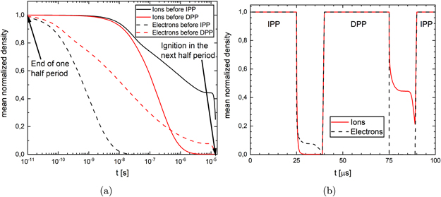
Figure 13. Mean normalized ion and electron density as a result of the diffusion and drift in the electric field generated by the applied voltage between the discharges in the two half periods calculated with COMSOL Multiphysics 5.5 plotted on a logarithmic time scale (a) and on a linear time scale (b). Since the absolute value of the density during the discharge was not calculated it was set arbitrarily to unity.
Download figure:
Standard image High-resolution image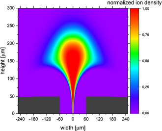
Figure 14. Space resolved normalized ion density before the ignition in the IPP as a result of the diffusion and drift in the electric field generated by the applied voltage after the end of the DPP calculated with COMSOL Multiphysics 5.5. The two nickel electrodes are again illustrated in gray.
Download figure:
Standard image High-resolution image3.2.3. Discharge ignition
The ignition was also investigated with side view imaging (amplitude 650 V, frequency 10 kHz, gate width 200 ns, exposure time 0.0125 s). Each image was taken 5 times. Afterward the average of these 5 images was calculated. This results in phase resolved images that were averaged over 625 periods.
Figure 15 shows four images from the ignition phase in the DPP. The color code shows for each image the minimal to maximal intensity of this image with the same order of the colors as in the previous graphs. As before these images are blurred because of the low depth of focus. The two black meshes indicate again the approximate position of the two nickel electrodes and the red mesh indicates the position of the dielectric foil. As soon as the discharge is ignited it emits light mainly from the bottom right corner of the channel (figure 15(a)). Since the electric field strength is the highest in the bottom corners of the channel (compare figure 4), the discharge is ignited here. From here the discharge moves up along the height of the channel by about 85 μm (figures 15(b) and (c)). It also shifts along the width of the channel from the right edge to the center. When the discharge reaches its maximal height, the intensity starts to decay again and the discharge pulse ends (figure 15(d)). Especially in figure 15(a) it looks like light is emitted from the inside of the dielectric foil. This is caused by the already discussed aberrations introduced by the optical system. Since the intensity is quite low in this image these aberrations become even more prominent. For completeness the actual complete measured images are shown here instead of suppressing the areas of the electrodes and the dielectric foil.

Figure 15. Four phase resolved side view images from the first discharge pulse in the DPP. The color code shows for each image the minimal to maximal intensity of this image with the same order of the colors as in the previous graphs. Normalized to image (a) the maximal intensity for the four images is (a) 1.00, (b) 2.23, (c) 2.37, (d) 1.27.
Download figure:
Standard image High-resolution imageFigure 16 shows four images from the ignition phase in the IPP. The color code shows again for each image the minimal to maximal intensity of this image with the same order of the colors as in the previous graphs. The discharge starts again to emit light from the inside of the channel (figure 16(a)). From here the discharge moves up along the height of the channel by about 50 μm (figures 16(b) and (c)). When the discharge reaches its maximal height, the intensity starts to decay again and the discharge pulse ends (figure 16(d)).
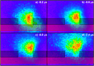
Figure 16. Four phase resolved side view images from the first discharge pulse in the IPP. The color code shows for each image the minimal to maximal intensity of this image with the same order of the colors as in the previous graphs. Normalized to image (a) the maximal intensity for the four images is (a) 1.00, (b) 2.13, (c) 1.64, (d) 0.77.
Download figure:
Standard image High-resolution imageIn both half periods the discharge starts to emit light from the inside of the channel after the ignition. In the IPP the discharge starts to emit light from a higher (about 50 μm) location than in the DPP. This is caused by the ions that are still left in the volume from the previous half period (compare figures 13 and 14). These ions provide now at the top of the cavity an additional contribution to the electric field strength. In the DPP no ions or electrons are left in the volume from the previous half period. Therefore, the discharge ignites here in a lower location than in the IPP. In both half periods the discharge moves up from its initial location along the height of the channel. The upper edge of the discharge is at the end of the first discharge pulse in both half periods on a similar height. Above this height the electric field strength is presumably no longer high enough to produce a significant number of electrons by electron impact ionisation. That is why the upper edge of the discharge stops in both half periods on a similar height.
4. Conclusion
The microplasma channel that was investigated in this work was designed to get new insights into the discharge dynamics of a microplasma array. Top view phase resolved images of the discharge in the microplasma channel revealed a similar behavior of the discharges in the microplasma channel and the microplasma arrays. Already known phenomena from the microplasma arrays like the self-pulsing, the asymmetric behavior of the discharge in the two half periods and the wavelike ignition were also observed in the microplasma channel. The observed propagation velocity was compared to estimated velocities for the drift and diffusion of the electrons and ions. Since the estimated velocities did not fit to the observed velocity a simple one-dimensional model for the propagation of the discharges along the length of the channel (across the array) was proposed. With this model it was possible to explain the different propagation velocities of the first discharges in one half period.
With the microplasma channel it was possible to resolve the emission structure of the discharge in all three dimensions for the first time. The side view phase resolved images show again the asymmetric behavior of the discharge in the two half periods. In the IPP the discharge extends over a larger width and a smaller height than in the DPP. The upper edge of the discharge is in both half periods on a similar height while the lower edge is in the DPP about 15 μm lower than in the IPP. These images confirmed the already proposed explanation for the asymmetric behavior. It is caused by the different direction of the electric field in the two half periods.
Additionally, the side view phase resolved images were used to investigate the ignition of the discharge in the two half periods. In the DPP the discharge ignites in the bottom corner of the cavity where the electric field strength is the highest. In the IPP the discharge ignites in a higher location. To explain this difference, a simulation of the diffusion and drift of the ions and electrons in the electric field was performed. This simulation showed that before the ignition in the DPP all ions and electrons from the volume have either reached one of the upper electrodes and recombined there or they have reached the top surface of the dielectric and adsorbed there as surface charges. Before the ignition in the IPP on the other hand there are still ions left over from the previous half period in the volume. These ions provide an additional contribution to the electric field strength at the top of the cavity and therefore the discharge ignites in the IPP in a higher location than in the DPP.
The discharges in the microplasma channel and the microplasma arrays behave in many aspects similar. However there are also some differences like for example the expansion of the discharge above the upper edge of the upper electrodes. These differences are most likely caused by the additional confinement of the cavities in the microplasma arrays and the resulting different three dimensional distribution of the electric field strength. Therefore, the general behavior of the microplasma channel that was observed in this work can be generalized for the microplasma arrays. The absolute values however may differ and one has to keep in mind that the two discharges are similar but still different. A microplasma array with a transparent upper electrode (e.g. made from indium tin oxide) could help to close the gap between the observations in the microplasma arrays and the microplasma channel.
Acknowledgments
This work was funded by the German Research Foundation (DFG) within the project A6 of the Collaborative Research Center CRC1316 'transient atmospheric plasmas: from plasmas to liquids to solids'.
: Appendix A.
In the following paragraphs some of the previous graphs are again presented for different measurements with microplasma channels with similar gap width. The absolute values vary slightly while the observed phenomena are similar for these measurements as already mentioned in section 2.2. The here presented graphs are just presented to reinforce the discussions above.
Figure 17 shows again the temporal development of the total emitted intensity (compare figure 5). The self pulsing of the discharge is again clearly visible. The frequency of the self pulsing was lower during this measurement (210 kHz instead of 300 kHz). The amplitude of the individual pulses decreases again and instead a more continuous emission is building up.

Figure 17. Temporal total light intensity development (black line) compared to applied voltage (red line). The intensity is measured by integrating over phase resolved side view camera images.
Download figure:
Standard image High-resolution imageFigure 18 shows the phase and space resolved emitted intensity of a different microplasma channel in the DPP (compare figure 8). The discharge ignites again at a few locations and propagates from there along the length of the channel. The propagation velocity for the individual discharges along the length of the channel is between (0.59 ± 0.17) km s−1 and (0.89 ± 0.21) km s−1. This is again similar to the velocities measured with the microplasma arrays. The self pulsing and transition to a more continuous emission in the later part of the half period is again clearly visible. For this microplasma channel the discharge ignites on one side (at length = 0 mm) about 8 μs earlier than on the other side. The intensity is also much larger on this side. This could be caused by a non uniform distance between the upper and the lower electrode by a slightly bended upper electrode.
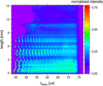
Figure 18. Phase space diagram of the discharge emission from the full channel in the DPP.
Download figure:
Standard image High-resolution imageFigure 19 shows the spatial resolved intensity distribution of the emitted light for the IPP and DPP, respectively (compare figure 11). Here the amplitude of the applied voltage was a bit higher than for the previous images (now 0.69 kV instead of 0.65 kV). As in the previous images the discharge expands in the IPP over a larger width and over a smaller height than in the DPP. The differences along the height are again mainly caused by the lower edge of the discharge while the upper edge is in both half periods on a similar height.

Figure 19. Side view false color intensity distributions as provided by the ICCD camera in IPP (left) and DPP (right). The electrodes and dielectric are again indicated by black and red meshes, respectively.
Download figure:
Standard image High-resolution image