TCAD Modeling of Surface Radiation Damage Effects: A State-Of-The-Art Review
 Arianna Morozzi
 Francesco Moscatelli
 Tommaso Croci
 Daniele Passeri
- 1Istituto Nazionale di Fisica Nucleare, Perugia, Italy
- 2CNR-IOM, Perugia, Italy
- 3Engineering Department, University of Perugia, Perugia, Italy
A comprehensive numerical model which accounts for surface damage effects induced by radiation on silicon particle detectors is presented with reference to the state-of-the-art Synopsys Sentaurus Technology CAD (TCAD) tool. The overall aim of this work is to present the “Perugia 2019 Surface” damage modeling scheme, fully implemented within the TCAD environment, which effectively describes the surface damage effects induced by radiation in silicon sensors relying on a limited number of parameters relevant for physics. To this end, extensive measurement campaigns have been recently performed on gated-diodes and MOS capacitors at Fondazione Bruno Kessler (FBK) in Italy, Hamamatsu Photonics (HPK) in Japan and Infineon Technologies (IFX) in Austria on both n-type and p-type substrates (with and without p-spray isolation implants), in order to extrapolate the relevant parameters which rule the surface damage effects. The integrated interface trap density and the oxide charge density, have been determined before and after X-ray irradiation with doses ranging from 0.05 to 100 Mrad(SiO2), for each specific foundry and technology flavor. The main guidelines of this study are the versatility and generality of the simulation approach.
Introduction
The planned Large Hadron Collider (LHC) upgrade to High Luminosity (HL) requires new generations of tracking detectors which have to efficiently operate in extremely harsh radiation environments [1,2]. The expected fluences and total ionizing doses (TID), integrated over 10 years of operation, are of the order of 2.2·1016 1 MeV neqcm−2 and 1 Grad for the innermost regions of the collider. The outermost layers will reach lower TID in the range of 10–70 Mrad, where evidence of saturation effects for the radiation induced damages are clearly visible. Definitely, one of the main challenges turn out to be the design of radiation tolerant silicon detectors to cope with the unprecedented increasing radiation doses and fluences. Hence, radiation hardness represents an essential requirement for sensors and therefore the radiation induced damage effects should be investigated with awareness.
Combined effects of surface and bulk damage will interplay in a significantly different manner depending on the particle interactions. The surface damage becomes more relevant if sensitive parts of the sensor chip are placed underneath or close to oxide layers (i.e. 3Ds and HV-CMOS sensors). Moreover, the trend of the break-down voltage depending on the dose is significantly affected by surface damage effects as well as the isolation in segmented detectors [3].
The overall aim of this work is to provide a modeling scheme, fully implemented within the TCAD environment, which effectively describes the surface damage effects induced by radiation in silicon sensors, relying on a limited number of physics meaningful parameters. To this end, extensive measurement campaigns have been recently performed on gated-diodes, MOS capacitors and MOSFETs fabricated at Fondazione Bruno Kessler (FBK) in Italy, Hamamatsu Photonics (HPK) in Japan and Infineon Technologies (IFX) in Austria on both n-type and p-type substrates (with and without p-spray isolation implants), in order to extrapolate the relevant parameters which rule the surface damage effects. The integrated interface trap density and the oxide charge density, have been determined before and after X-ray irradiation with doses ranging from 0.05 to 100 Mrad(SiO2), for each specific foundry and manufacturing process. Acceptor-like and donor-like interface states characteristics have been investigated by exploiting devices fabricated on both polarity substrates.
The versatility and generality of the simulation set-up represent the main guidelines of this study. Indeed, not only different design options/detector geometries can be evaluated, but also different vendors and/or technology options can be investigated. When numerical simulations are capable of verify experimental results, they will also gain predictive power, resulting in reduced time and cost in detector design, development and optimization.
Surface Radiation Damage Effects
Surface damages are mainly related to ionization effects. A net result of ionization processes is the build-up of a positive charge within SiO2 layers and the creation of defects localized at the SiO2/Si interface. Surface damage is responsible for the surface generation current variation and strongly impacts on the breakdown voltage, the inter-electrode isolation and capacitance, and might also affect the charge collection properties of solid-state sensors. SiO2/Si interface defects are typically referred as amphoteric, due to their dual nature as they simultaneously behave as donor-like and acceptor-like traps by interacting with both free holes and free electrons [3,4]. From a physical point of view, this means that acceptor-like (donor-like) defects behave in analogy to shallow level impurity states associated with acceptor (donor) dopant atoms and, hence are negatively charged (neutral) when occupied by electrons and neutral (positive charged) when empty. As a consequence, interface defects can be effectively evaluated by looking at the donor-like trap states effects on devices manufactured on p-type substrates (p-type MOS capacitors, n-on-p GDs) and pMOSFETs and at acceptor-like trap states effects from measurements on n-type substrate devices (n-type MOS capacitors, p-on-n GDs) and nMOSFETs [5].
Radiation damage effects severely influence the electrical response of silicon sensors both in terms of static and active behavior (e.g. charge collection efficiency) as a function of the dose. A thorough understanding of the macroscopic effects related to damage is of utmost importance to devise a physics meaningful modeling scheme which has predictive capabilities on the electrical behavior of irradiated silicon sensors.
This work aims at describing the state-of-the-art “Perugia 2019 Surface” damage modeling scheme from its development phase to its application stage. The pursued procedure is to find out the main significant dose-dependent parameters capable of describing the surface damage effects, starting from C-V and I-V measurements performed on dedicated test structures at different X-ray irradiation doses. The experimental procedure that followed is based on the methodologies mainly proposed by Nicollian and Brews [5] and by McWorther and Winokur [6]. In particular, the oxide charge density QOX (cm−2), the interface trap states density DIT (cm−2 eV−1) for acceptor and donor trap states and the integrated interface trap density NIT (cm−2) have been straightforwardly assessed from measurements and represent the main measurable key quantities to evaluate the surface damage extent. In a previous work [7], the extrapolation of all these quantities has been described in detail, as well as their dependence on the irradiation dose. In addition, their values depend on the irradiation conditions (e.g. dose, dose rate), biasing conditions during irradiation and post-irradiation processes (e.g. time/temperature of annealing).
The X-Ray Irradiation Campaign
The X-ray irradiation campaign was carried out at the Department of Physics and Astronomy at the University of Padova in Italy at room temperature with doses ranging from 0.05 to 100 Mrad(SiO2). X-rays energies were in the range of 8–40 keV. The X-ray spectra emitted from the tube was additionally filtered for total dose tests by 0.15 mm thick Al sheet in order to attenuate the low-energy (<8 keV) component [8]. The dose rate was 0.8 Mrad per hour. The X-ray dose is customarily referred to the silicon dioxide, since the radiation damage is mainly quantified by the charge produced in the dielectric layer.
Current-Voltage (I-V) and Capacitance-Voltage (C-V) measurements were performed with a computer-controlled parametric system which is mainly based on a semiautomatic probe station with a Keithley K707 switching matrix, a Keithley K90 I-V measuring system and a Keithley K82 C-V measuring system. When measuring capacitances, we corrected for the dissipation factor D. The assessed values for D were small, as well as the series resistance. The measurement procedure consists of measuring at least three times to ensure precision and repeatability.
Description of the Test Structures Under Investigation
The properties of the SiO2 layer and of the SiO2/Si interface were thoroughly investigated on high resistivity silicon test structures exposed to X-ray irradiation with doses in the range of 0.05–100 Mrad(SiO2). Extensive measurements have been performed on MOS capacitors, MOSFETs and gated-diodes fabricated at FBK, HPK and IFX on both n-type and p-type substrates (with and without p-spray isolation implants), in order to extrapolate the relevant parameters which rule the surface damage effects.
For an identical technology process, the simultaneous irradiation of devices fabricated on both polarity substrates allows the identification of acceptor and donor trap states, which fully characterize the entire silicon energy gap. The envisioned measurement methodology enables the cross-check comparison between measurements carried out e.g. on GD, MOS capacitors made on n-type substrates and nMOSFETs (assess acceptor-like DITacc), and GD, MOS capacitors made on p-type substrates (assess donor-like DITdon).
For the sake of clarity and completeness, Figure 1 shows the experimentally assessed acceptor-like and donor-like interface trap states and the oxide charge density as a function of the X-ray dose. These quantities have been obtained by averaging measurements performed on FBK MOS capacitors, gated-diodes and MOSFETs realized on both p-type and n-type substrates without bias during irradiation. The small measurement error, even for high doses, confirm the validity of the experimental procedure to investigate surface damage effects. Both QOX and NIT increase with increasing radiation levels up to about 10 Mrad(SiO2) after which start to show a saturating behavior despite the dose increasing.
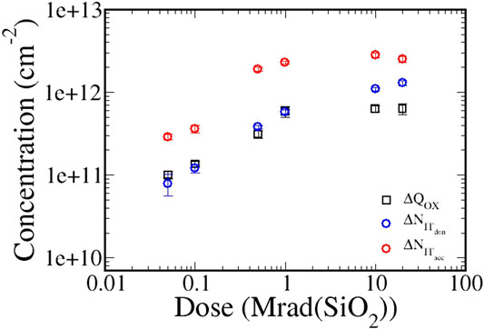
FIGURE 1. Radiation induced oxide charge density increase ΔQOX (cm−2) and acceptor-/donor-like integrated interface trap states density increase ΔNIT (cm−2) depending on the irradiated dose. They have been obtained by averaging measurements performed on FBK MOS capacitors, gated-diodes and MOSFETs realized on both p-type and n-type substrates. No bias during irradiation.
Aiming at developing a physics meaningful numerical modeling scheme which accounts for the surface damage effects on silicon sensors, our starting point were the experimental measurements performed on different test structures fabricated with identical technology processes. The following sub-paragraphs describe the specific measurements and the pursued experimental methodologies to extrapolate the quantities related to surface damage effects, depending on the particular device under test. For a more detailed description of the methodology, refer to the cited works in each sub-paragraphs in which the measurement and extraction procedures have been described in their entirety. The values of QOX, NITacc, and NITdon thus obtained, have been used as input parameters for the development of the comprehensive “Perugia 2019 Surface” analytical model specific for each technology process [7,9–13]. Moreover, from the DITacc and DITdon profile, the energy distribution of the acceptor-like and donor-like interface defects has been assessed. The pursued procedure made it possible to conceive a predictive modeling scheme, fully implemented within the TCAD environment, with solid experimental basis. The developed analytical model has been than validated against experimental measurements of different devices for each specific fabrication technology, as thoroughly described in the next sections.
MOS Capacitors
MOS capacitors represent simple devices widespread used to study the semiconductor surface behavior after radiation damage. In fact, a wealth of information about the structure itself and the quantities related to surface damage effects can be obtained from C-V measurements. In general, ionizing radiation effects result in the increase of both trapped oxide charge and interface traps. On the one hand, the oxide fixed charge within SiO2 is immobile under an applied electric field, predominantly positive and therefore cause an overall shift of the flat-band voltage (VFB) toward more negative values with increasing irradiation dose exposure. In fact, the flat-band voltage shift due to irradiation can be precisely assessed from measurements and it is directly ascribable to a precise amount of QOX increase at the oxide/silicon interface [7]. On the other hand, the SiO2/Si interface is also characterized by amphoteric interface traps distributed throughout the silicon energy gap. From a macroscopic point of view, they induce a stretching-out in the high-frequency capacitance-voltage curve depending on the imparted X-ray irradiation dose.
The interface trap states density DIT can be instead estimated by means of the capacitance High-Low Method, which is based on the charging kinetics of interface traps [5]. Indeed, interface traps contribute to capacitor charging current in quasi-static measurements. Since their time constants are relatively long, their effect is greatly reduced or even absent in HF measurements. As a consequence, the difference between quasi-static (QS) and high-frequency (HF, 100 kHz) capacitance-voltage measurements under depletion condition allows the direct determination of the dose dependent value of DIT for acceptor-like and donor-like interface traps [5]. This method provides a reliable estimate of DIT for energy values between mid-gap and 0.2–0.3 eV from the reference band edge (i.e. conduction band for acceptor and valence band for donor trap states). The behavior in the region closer the conduction/valence band can be therefore deduced by looking at the DIT trend.
As an example, Figures 2A,B show the measured profile for the acceptor-like interface state density (DITacc) and donor-like interface state density (DITdon), obtained by means of the High-Low Method for FBK test structures. Figure 2A highlights a uniform behavior of DITacc all along the considered energies and for all the evaluated X-ray irradiation doses. From the behavior analysis, it is possible to assume that DITacc remains approximately constant approaching the conduction band edge. Unlike the previous case, each curve reported in Figure 2B tends to decrease as approaching the valence band edge irrespective of the irradiation doses, thus leaving a relatively low interface trap state density in this region. The analysis of the acceptor-like and donor-like interface traps states density trend was of fundamental importance for the development of the “Perugia 2019 Surface” model which fully reflects the outcomes of this behavioral analysis. Indeed, two uniform bands of defects, one acceptor and one donor have been implemented within the TCAD environment with a DIT profile compatible with the experimental one. The integration of DIT over the suitable energy range gives NIT as a result, which represent the input quantity to the TCAD radiation damage modeling scheme, together with the QOX.
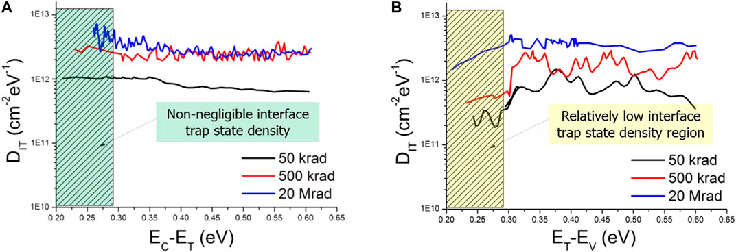
FIGURE 2. Acceptor-like interface state density DITacc (cm−2eV−1) measured on n-type MOS capacitors (A), donor-like interface state density DITdon (cm−2eV−1) measured on p-type MOS capacitors (B), exposed to 0.05, 0.50 and 20 Mrad(SiO2).
All these effects were investigated on MOS capacitors manufactured by the three different vendors taken into account and the assessment of the radiation induced effects was reported in related previous works [7,12,14].
MOSFETs
Information about the SiO2/Si interface trap states can be also extrapolated from the transfer characteristics of MOSFETs. Indeed, combined effects of oxide charge and interface traps can be disentangled by means of specific data analysis procedure to apply on the subthreshold-current curve of a MOSFET in saturation [7,12,14]. The irradiation induces a shift in the threshold voltage (ΔVTH). By means of the method proposed by McWhorter and Winokur [6] it is possible to separate the measured ΔVTH into a contribution due to the interface traps density increase (ΔNIT) and a contribution due to the trapped oxide charge density variation (ΔQOX). Basically, the contribution of ΔQOX to the threshold shift closely depends on the given irradiation dose and the macroscopic overall effect is a solid translation of the entire characteristics toward higher gate voltage for increasing doses. In addition, the portion of the subthreshold current curve between the threshold-voltage and the midgap-voltage shows a stretching-out behavior. This stretching-out strictly depends on the given X-ray dose and it can be therefore directly attributed to a given amount of ΔNIT.
Gate-Controlled Diodes
The surface generation velocity s0 is directly proportional to the integrated interface trap states density NIT and can be easily assessed from I-V measurements performed on gated-diode devices [12,15,16]. The conventional measurement procedure consists in analyzing the diode current by sweeping the gate voltage from inversion to accumulation, while keeping the p-n junction at a constant reverse bias. The surface current (Isurf) is the difference between the current in depletion and in inversion and it tends to increase with the absorbed X-ray dose increase. The same trend is necessarily followed by the surface generation velocity as well, since s0 is directly proportional to the surface current. In addition, the flat-band voltage of GDs subjected to X-ray irradiation shifts progressively toward negative values, being the macroscopic evidence of the trapped oxide charge density rising at the oxide/silicon interface. Further details about the procedure to extrapolate the radiation induced increase in NIT and QOX are explained in detail in [7].
TCAD Device-Level Simulation Environment
State-of-the-art TCAD simulation tools at device/circuit level offer a wide variety of approaches for the analysis of semiconductor devices, balancing physical accuracy and comprehensiveness, application versatility and computational demand. The available portfolio of approaches emphasizes the complexity of the problem of devising a reliable model, suitable for prediction analyses and accounting in a comprehensive way, for complex phenomena such as the radiation damage effects.
The “Perugia 2019 Surface” modeling scheme accounts for the surface damage effects on silicon sensors up to radiation damage levels expected at HL-LHC (e.g. greater than 2.0 × 10¹⁶ 1 MeV equivalent neutrons/cm2). Its predictive capabilities in terms of electrical responses of silicon sensors enable its use for the investigation and optimization of irradiated devices fabricated by different vendors (e.g. with different technology flavors) and in different operating conditions (e.g. at different fluences, temperatures and biasing voltages). The “Perugia 2019 Surface” modeling scheme is fully implemented within the Synopsys©Sentaurus TCAD environment. At the development stage, a physics grounded approach has been pursued aiming at keeping the number of fitting parameters as low as possible, thus devising a not overspecific modeling scheme.
For TCAD simulation purposes, the surface radiation damage effects can be ascribed to the building up of trapped charge within the oxide (QOX) and the increase in the number of interface trap states (NIT). With traps we refer to allowed energy states within the semiconductor energy gap, which affect the electrical behavior of the silicon sensor to many respects: alteration of the effective doping, enhancement of generation/recombination process and increase in leakage current. From TCAD standpoint, traps are described by defining their type (acceptor or donor), their energy distribution (Level, Gaussian, Uniform, ...), their capture cross-sections for both holes and electrons and their concentration. In particular, acceptor traps are considered uncharged when unoccupied (empty) or negatively charged when occupied. On the other hand, donor traps are uncharged when unoccupied (empty) or positively charged when occupied. Even if traps located in the upper half of the energy gap energy are usually assumed as acceptors and traps located in the lower half are assumed as donors, the trap type definition should be carefully taken into account, in particular when describing interface trap states which typically act as amphoteric defects.
TCAD Numerical Model for the Radiation Damage
Damage effects induced by radiation have been systematically studied for decades, since they seriously limit the semiconductor detector’s lifetime. Concerning the surface damage effects, different TCAD modeling approaches have been developed and applied in the past as the one proposed by Peltola which took into account the build-up of a fixed charge within SiO2 layers only, for increasing irradiation doses [17]. Then different models also integrated the interface trap states density highlighting the need for a correct trap parameterization and the complexity for the determination of the interface defects [18,19]. Other models of the surface damage effects consider the fixed oxide charge and takes into account NIT by means of the surface velocity parameter [20–22].
Since from the early stages, the modeling scheme for the surface damage effects developed at the University of Perugia envisaged both the radiation induced oxide charge and the interface trap states. The interface states were initially modeled with three single trap levels, one donor at 0.60 eV from the valence band edge (EV) and two acceptors at 0.40 eV and at 0.60 eV from the conduction band edge (EC), respectively. The overall trap states density NIT for acceptor and donor was the same for both trap types, at a specific dose. In particular, for any given acceptor density NIT, the 60% of acceptors traps were allocated at ET = EC − 0.60 eV, while the remaining 40% were allocated at ET = EC − 0.40 eV. The ratio NIT/QOX was in the range of 0.70–0.85 and the capture cross sections of all defects were fixed at 1.0 × 10⁻¹⁵ cm2 [23].
By carefully considering the measured spectral density distribution of DIT, extracted by means of the capacitance C-V High-Low method, a more physics meaningful modeling of the interface traps was developed. The overall DIT was then modeled by a convolution of three Gaussian distributions with the same standard deviation, two for the acceptor-like and one for the donor-like interface trap states, centered on the energy levels considered with the previous model [7,24,25]. The modeling scheme with gaussian shaped trap states was extensively validated by means of the comparison with interstrip resistance measurements. However, its predictive capability, granted for interstrip resistance even for high doses, was not suitable for other types of devices (e.g. MOS capacitors, gated-diodes, … ).
Generality and flexibility represent the ultimate goal of developing a comprehensive TCAD numerical model for the surface damage effects. To this purpose, the “Perugia 2019 Surface” damage modeling was therefore improved, aiming at balancing complexity and comprehensiveness. The updated version in 2019 took shape after extensive measurement campaigns carried out on dedicated test structures provided by three principal vendors of solid-state particle detectors (FBK, HPK, IFX) before and after irradiation with X-rays in the range of 0.05–100 Mrad(SiO2). On the basis of the experimentally obtained energy distribution of the interface trap state density (Figures 2A,B), the previously developed TCAD numerical model was modified, by reducing the number of fitting parameters and closely tightening their numerical values to the experimentally assessed ones. The new modeling scheme is summarized in Table 1. It features two uniform trap energy distribution bands, one for donor- and one for acceptor-like defects. ET represents the mid energy-level of the uniformly distributed band of trap, while EC and EV are respectively the conduction and the valence band edges. Accordingly to measurements, the energy width of the two bands is different, as well as the values of the interface trap densities related to acceptor states DITacc (measured on n-type substrates) and to donor states DITdon (measured on p-type substrates), which are uniformly distributed along the considered energy bands and strongly depend on the given X-rays dose. In fact, the acceptor-like band uniformly extends from the conduction band edge to mid-energy gap, while the donor-like one starts from the valence band edge and ends 0.60 eV far from it. Conventionally the reference quantity for the interface trap states is the integrated value of the density NIT. This modeling scheme is independent of the technology flavor, while the amount of interface trap states and oxide charge density strictly depends on the specific manufacturing technology process. Indeed, the model remains the same when simulating different technology processes (e.g. the width of the bands does not vary), while the traps parameterization varies congruently with the analytical laws described in the next section (Tables 2–5). With traps parameterization we refer to the values assumed by the acceptor/donor traps and the value of the oxide charge densities at a specific dose. The traps parameterization is assessed by means of irradiation and testing campaigns on simple test structures, from which NIT and QOX can be straightforwardly extrapolated. The strength of this approach is that, once the parameterization in known, it is possible to apply the modeling scheme to predict the electrical behavior of more complex sensors, since the extent of the damage is the same for the same technology regardless of the device.
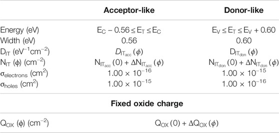
TABLE 1. Details of the “Perugia 2019 Surface” damage modeling scheme.
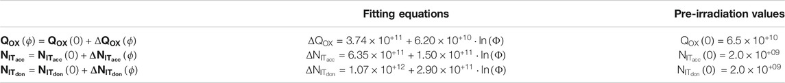
TABLE 2. Fitting equations and pre-irradiation values for “Perugia 2019 Surface” modeling HPK silicon devices: oxide charge QOX (cm−2), acceptor interface trap states NITacc (cm−2), donor interface trap states NITdon (cm−2).
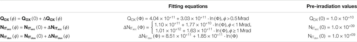
TABLE 3. Fitting equations and pre-irradiation values for “Perugia 2019 Surface” modeling IFX eight″ silicon devices: oxide charge QOX (cm−2), acceptor interface trap states NITacc (cm−2), donor interface trap states NITdon (cm−2).

TABLE 4. Fitting equations and pre-irradiation values for “Perugia 2019 Surface” modeling IFX 6″ silicon devices: oxide charge QOX (cm−2), acceptor interface trap states NITacc (cm−2), donor interface trap states NITdon (cm−2).

TABLE 5. Fitting equations and pre-irradiation values for the “Perugia 2019 Surface” modeling FBK silicon devices: oxide charge QOX (cm−2), acceptor interface trap states NITacc (cm−2), donor interface trap states NITdon (cm−2).
At each radiation dose, both the oxide charge density and interface trap state density are modeled as the sum of the value before irradiation (NIT (0) and QOX (0)) and the radiation induced increase (ΔNIT(Φ) and ΔQOX(Φ)). This approach enables a more realistic assessment of the surface damage extent by considering a small amount of fixed oxide charge and interface trap states even in non-irradiated devices, as a result of the fabrication processes. From measurements, the experimentally assessed values for QOX, NITacc and NITdon have been then used as input parameters for the traps parameterization which describes their trends as a function of the X-ray dose. This enables the suitability of performing predictive analyses at different doses from the investigated ones.
The new interface modeling scheme has been implemented within the TCAD environment (Supplementary Appendix A) and then used to evaluate the C-V behavior of MOS capacitors, the I-V characteristics of gated-diodes, as a function of the dose. This model proved to be technology-independent and non overspecific and has been validated on both n-type and p-type substrate devices, as described in the next sections. Thanks to the simulation approach it has been possible to disentangle the combined effects of the oxide charge density from the acceptor/donor interface trap states density to identify the most sensitive technological parameters to be optimized for the design of advanced silicon radiation detectors and their performance prediction. It is eventually possible to evaluate the impact, in terms of electrical behavior, of different technology/process options resulting in different oxide and silicon/oxide properties. This fosters the application of numerical TCAD modeling as a tool to investigate the trapping/detrapping mechanisms behind silicon radiation damaging, aiming at the optimization of particle detector radiation resistance.
Synopsys Sentaurus TCAD device simulator has been used for the purpose at hand, by performing static (DC), and small-signals (AC) analyses. As a starting point, a TCAD sensitivity analysis to the variations of the main model’s parameters has been carried out. The main results were reported in recent works where the separated effects of QOX variation only, or of the acceptor/donor NIT variation only, were considered on C-V curves of p-type/n-type MOS capacitors and on I-V characteristics of gated-diodes [9,26]. The approach of selectively considering a single component of the surface radiation damage model allows a proficient study of the interplay between QOX and NIT on irradiated silicon sensors, fostering a correct interpretation of measurements. This in turn, enables a deep investigation of the complex physical phenomena behind the radiation damage effects in solid-state silicon sensors. This stage turned out to be crucial for the development of the final system of analytical equations which rule the increment of QOX and NIT on silicon sensors depending on the manufacturing process (e.g. vendor, technology). In order to validate the radiation damage model, several comparisons have been carried out between simulation results and measurements on actual devices. A huge number of test structures have been irradiated and measured, and data from literature have been collected as well, as it will be illustrated in the following.
Comparison With Experimental Data
HPK Test Structures
Hamamatsu Photonics devices were fabricated on high-resistivity p-type Float Zone (FZ) wafers, with two different options: 1) HPK p-spray including a p-spray isolation implant all over the wafer, 2) HPK p-stop where isolation p-implants are confined in dedicated wells between n+ collection regions. For test structures measurement purposes (e.g. MOS capacitors, gated diodes), this corresponds to a presence (p-spray) or to the absence (p-stop) of a p-spray layer underneath the oxide layer. The oxide nominal thickness is 700 nm.
Analytical Model
The overall amount of QOX, NITacc, and NITdon rule the surface damage effects at a specific X-ray dose. These quantities are strictly technology dependent and they have to be fed as input to the TCAD simulator, accounting for surface damage effects. In general, they vary with dose and can be modeled as the sum of the starting value (i.e. non-irradiated device) summed with the increment (Δ) induced by the irradiation, namely:
(Δ)QOX (Δ)NITacc and (Δ)NITdon are expressed in cm−2 and Φ in Mrad.
The QOX, NITacc, and NITdon increase trends for HPK devices as a function of the dose are reported in Figures 3A–C, respectively and have been selected to devise the interpolating curves. The whole set of parameters have been extrapolated from the different test structures, namely MOS capacitors and gated-diodes designed on p-type substrates (with and without the p-spray isolation layer). An analytical model has been derived from these data, thus enabling predictive analyses at different doses from the investigated ones. The oxide charge density and the acceptor- and donor-like interface traps tends to increase with the increasing dose, until reaching a saturation trend. The corresponding equations and the pre-irradiations values for all the parameters are reported in Table 2. These values represent the input parameters to implement the “Perugia 2019 Surface” damage modeling scheme within the TCAD environment, accounting for the SiO2/Si interface and enabling the prediction of the electrical behavior of irradiated HPK sensors.
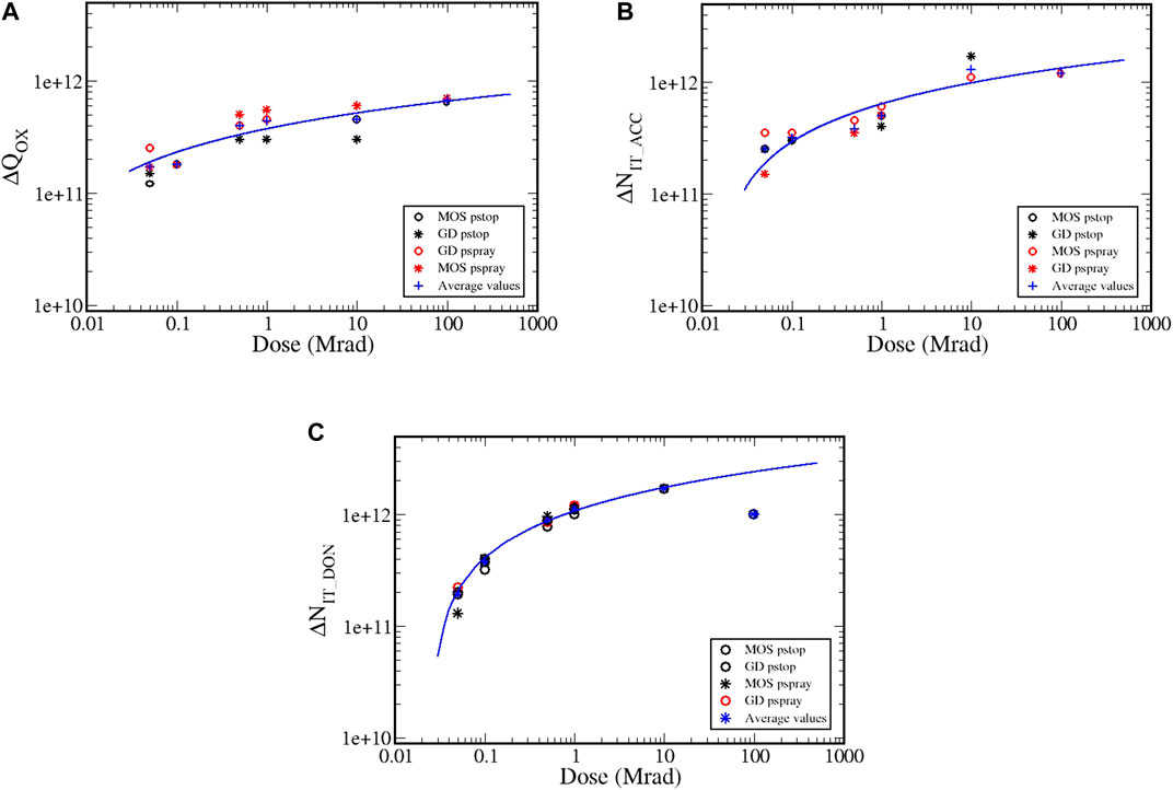
FIGURE 3. Input parameters (fitting curves) for “Perugia 2019 Surface” modeling HPK silicon devices: (A) Oxide charge density increase. (B) Acceptor-like interface trap state density increase (C) Donor-like interface trap state density increase.
Simulation Results
The simulated MOS device is a 2D approximation of a cylindrical MOS capacitor. The actual device dimensions have been considered by appropriately setting a geometrical area factor AF (
The C-V characteristic of MOS capacitors has been selected as the main figure of merit for the TCAD surface radiation damage effects model validation. The high-frequency (HF) capacitance is obtained from a small signal capacitance measurement at a frequency of 100 kHz and it reflects the charge variation within the depletion layer as a function of the gate voltage. Conventionally, C-V data are normalized to the geometrical measured oxide capacitance COX. In order to improve the plots clarity, besides reporting all sets of measurements, the average of at least three measurement sets has been selected as reference at a given irradiation dose. In all pictures reported below, the solid lines are used to symbolize the measurements while the dashed lines represent the simulation findings.
All measurements were carried out under the same thermal conditions, hence at 20 °C after an annealing at 80 °C for 10 min, as common practice [27,28]. Further details about the experimental procedure and measurement set-up are explained in detail in previous related works [7,12,24].
The “Perugia 2019 Surface” damage model has been applied to the investigation of irradiated HPK test structure devices with doses from 0.05 to 100 Mrad(SiO2) [10,11,14]. Figures 4, 5 show the comparison between the simulated and measured C-V characteristics of HPK MOS capacitors with and without a p-spray isolation layer. The TCAD numerical model is capable of well reproducing the measurement curves, thus strengthening the suitable characterization of the SiO2/Si properties. The presence of the p-spray layer significantly impacts on the tested devices performance. Indeed, the capacitance excursion from inversion to accumulation is much less than the C/COX excursion in p-type MOS capacitors without the p-spray implant, because of the smaller depleted layer.
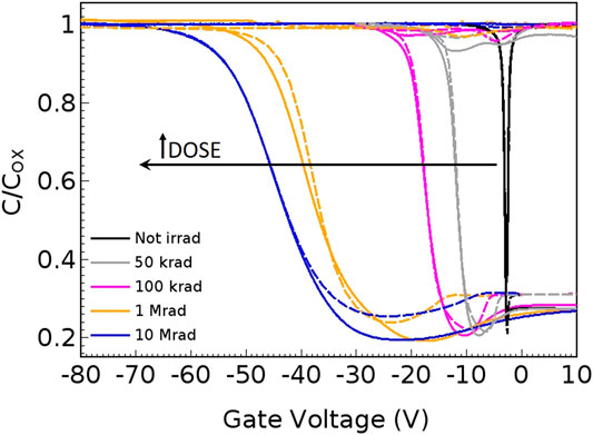
FIGURE 4. C-V characteristics of HPK MOS capacitors: comparison between measurements and simulations (no p-spray isolation layer). Measurements in solid line and simulations in dashed line.
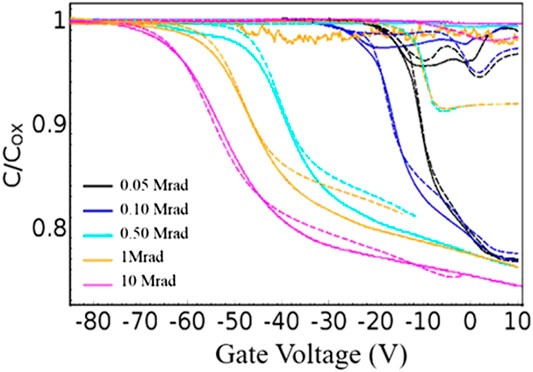
FIGURE 5. C-V characteristics of HPK MOS capacitors: comparison between measurements and simulations (with p-spray isolation layer). Measurements in solid line and simulations in dashed line.
The generality of the developed modeling scheme has been verified by simulating different type of test structures, namely gated-diodes. The considered devices under test for irradiations and measurements feature a 240 µm depth p-type substrate with or without a p-spray implant. Figures 6, 7 illustrate the comparison between the measured and simulated diode current as a function of the bias voltage applied to the gate contact carried out on HPK gated-diodes. The overall agreement between measurements and simulations is more than satisfactory. Moreover, the difference between the maximum current value in depletion region and the average current in accumulation, which is directly related to the surface recombination velocity [7], is very well reproduced for all the available irradiation doses.
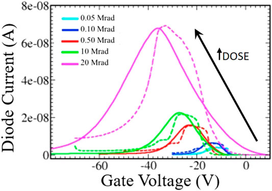
FIGURE 6. I-V characteristics of n-on-p HPK gated-diode: comparison between the measured and simulated diode current as a function of gate voltage (no p-spray isolation layer).
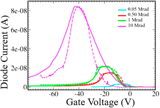
FIGURE 7. I-V characteristics of n-on-p HPK gated-diode: comparison between the measured and simulated diode current as a function of gate voltage (with p-spray isolation layer).
IFX Test Structures
Devices under study include MOS capacitors exploiting different technology options. In particular, for Infineon Technologies two different processes have been characterized: 1) IFX high-resistivity p-type Float Zone (FZ) 8 inch wafers; 2) IFX high-resistivity p-type Float Zone (FZ) 6 inch wafers with different processes and thermal budget to produce test structures. The nominal oxide thickness is 550 nm for both the processes.
Analytical Model
The measured trends of the QOX, NITacc and NITdon increase with the dose have been thoroughly taken into account for 8″ and 6″ Infineon Technologies silicon devices. The resulting interpolating curves can be used for deriving the exact parameters values to be used for the simulations, depending on the selected doses. To this purpose, the corresponding equations and the pre-irradiations values for all the parameters are reported as well in Tables 3, 4.
Concerning the IFX 8″ silicon devices, it is worthwhile to notice that the increase of the NITacc follows two different trends depending on the X-rays irradiated dose above or below 1 Mrad(SiO2). Indeed, a threshold behavior around 1 Mrad(SiO2) emerged from the experimental data thus making not possible to model this parameter with a single analytical function. The radiation induced increase of QOX for IFX 6” silicon devices shows the same behavior. In this last case, the oxide charge density increases linearly with dose for doses lower than 1 Mrad(SiO2). For higher doses the radiation induced increment, tends to saturation.
The developed analytical model represents a powerful tool to predict the behavior of electronic devices at doses higher than those at which they were actually irradiated. Despite the X-rays irradiation doses were in the range of 0.05–100 Mrad(SiO2), it is possible to study different doses from the measured ones.
Simulation Results
A comprehensive comparison between simulations findings and measured data in terms of C-V characteristics of MOS capacitors is shown in Figures 8, 9 for the two different IFX manufacturing processes. The agreement between measurements (solid lines) and simulations (dashed lines) is very good in accumulation and depletion regions, where the High-Low Method allows to measure with high precision the interface trap density. In inversion, the measurement error is too high to precisely evaluate the interface trap density [5], therefore a relatively high discrepancy between measurements and simulations can be expected and accounted for. The good agreement between simulations and measurements was demonstrated even in recent works [10,11,14].
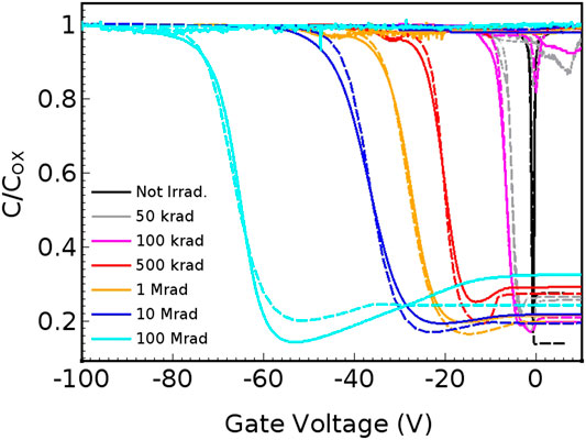
FIGURE 8. C-V characteristics of IFX MOS capacitors: comparison between simulated and experimental data for 8″ process (solid line measurements, dashed lines simulations).
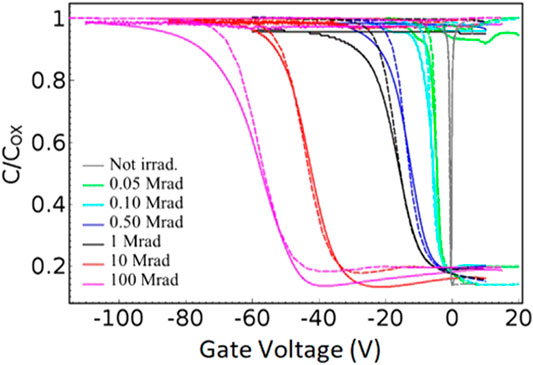
FIGURE 9. C-V characteristics of IFX MOS capacitors: comparison between simulated and experimental data for 6″ process (solid line measurements, dashed lines simulations).
The strength of this developed surface model relies on the flexibility of use with respect to the manufacturing technology. Indeed, despite the value of interface trap states and consequently the flat-band voltage shifts at increasing irradiation doses are different for the two manufacturing processes, a unique modeling scheme is capable of reproducing the measured data after a proper setting of the oxide charge and interface trap states. For both the technology options, the flat-band voltage is correctly reproduced in all the simulated C-V curves at all the considered doses, thus consolidating a proper description of the QOX. The reproducibility of the measured slope of the curves in depletion ensures the correct parameterization of NIT.
FBK Test Structures
Devices under study include MOS capacitors and gate-controlled diodes manufactured at Fondazione Bruno Kessler (FBK, Italy) on 6” n-type and p-type SiSi Direct Wafer Bonded Wafers from ICEMOS Technology Ltd [29]. The active layer is a Float Zone <100> wafer, with a nominal resistivity higher than 3 k Ωcm. The nominal oxide thickness is 300 nm for p-in-n and 700 nm for n-in-p test structures. Moreover, the n-in-p fabrication technology considers a p-spray layer implanted at the surface to isolate adjacent n+ collecting regions. Since sensors (e.g. pixels, strips) and test structures were processed on the same wafer, the radiation induced surface damage effects investigated for test structures can be safely extended to the sensors case.
Analytical Model
The analytical model which accounts for the radiation induced increase of QOX, NITacc and NITdon for the simulation of FBK silicon sensors and the corresponding equations and the pre-irradiations values for all the parameters are reported in Table 5. The interpolating curves arise from the parameters extrapolated from FBK MOS capacitors and gated-diodes manufactured on both n-type and p-type substrates with p-spray layer of isolation. These parameters can be therefore used for deriving the exact values to be used for the simulations, depending on the X-ray dose.
From experimental data emerges how the surface damage effects are independent of the strip isolation strategy [12]. Indeed, the QOX and NIT values extrapolated from MOS capacitors with and without the p-spray layer are very close.
Simulations Results
The FBK test structures irradiation campaign has been limited to 20 Mrad(SiO2) trying to find a balance between number of different test structures and time of exposure. Although the considered irradiation doses are lower than the expected total ionizing doses at the end of HL-LHC operation (1 Grad), nevertheless the obtained results can be used to infer the surface damage effects for higher doses. Indeed, saturation effects of NIT and QOX can be already noticed at 10–20 Mrad [12].
Figure 10 shows the comparison between simulated and measured QS and HF C-V characteristics for n-type MOS capacitors. The measured oxide capacitance (COX) is well reproduced by the simulated low frequency capacitance in both the accumulation and inversion regimes. Quasi-static measured capacitance values are very precisely reproduced by simulations, even at higher doses where they have an almost flat behavior. This indicates that the interface states densities have been accurately described within the TCAD environment. Furthermore, the simulated high-frequency capacitance follows, with a high accuracy level, the charge variations within the depletion layer all along the applied gate voltages, thus demonstrating the suitability of the “Perugia 2019 Surface” modeling scheme for the description of the electrical behavior of simple test structures. Eventually, the measured and simulated QS and HF capacitances as a function of the gate voltage, are in good agreement for all the considered irradiation doses.
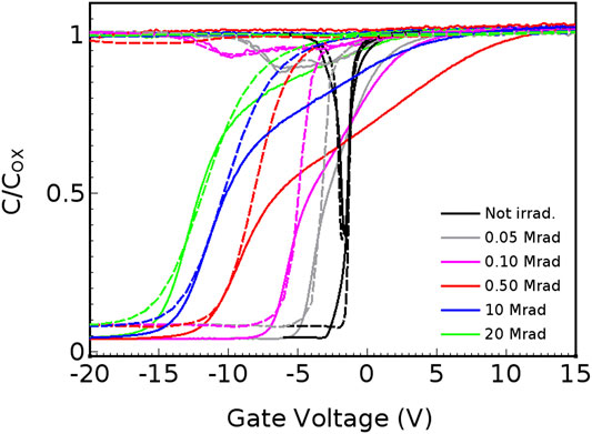
FIGURE 10. C-V characteristics of FBK n-type MOS capacitors irradiated with Xray doses of 0.05, 0.10, 0.50, 10, 20 Mrad(SiO2): comparison between measurements (solid lines) and simulations (dashed lines).
The TCAD numerical model for the surface damage effects has been then applied for the analysis of QS and HF C-V characteristics of p-type MOS capacitors with a p-spray layer implanted at the surface. Figure 11 illustrates the simulation results. The presence of the p-spray layer has a significant impact on the electrical behavior of these tested devices. By sweeping the gate voltage from inversion to accumulation the capacitance excursion values are much less than the C/COX excursion in n-type MOS capacitors and this is due to the lower depleted layer. The presence of the p-spray introduces a not negligible uncertainty for the capacitance values in inversion for doses higher than 0.50 Mrad(SiO2). However, the flat-band voltage values are well reproduced for all the considered X-ray doses, thus showing that the QOX increase at the oxide/silicon interface has been accurately modeled. Indeed, in MOS capacitors the flat-band voltage shift due to irradiation can be directly ascribable to a precise amount of QOX increase at the oxide/silicon interface.
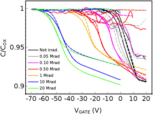
FIGURE 11. C-V characteristics of FBK p-type MOS capacitors and after X-ray doses of 0.05, 0.10, 0.50, 1, 10, 20 Mrad(SiO2): comparison between measurements (solid lines) and simulations (dashed lines).
To further support the robustness and flexibility of the modeling scheme for the simulation of irradiated silicon sensors, the model has been applied to the study of the static behavior of irradiated gated-diodes. Figure 12 shows the comparison between the measured (solid lines) and simulated (dashed lines) diode current as a function of the applied gate voltage for gated-diodes irradiated at 0.05, 0.5, 1, 10, and 20 Mrad(SiO2). The experimental diode current trend is very well reproduced, thus highlighting the predictive capability of the numerical modeling scheme in reproducing the electrical behavior of different typologies of devices and processes. The main simulation goal of gated-diodes consists in the surface generation velocity prediction at high irradiation doses. This goal has been largely achieved, as reported in Table 6 where the experimentally assessed surface generation velocity and the simulated one have been listed for all the considered doses.
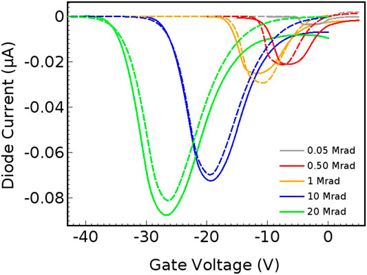
FIGURE 12. I-V characteristics of p-on-n FBK GD irradiated with X-ray doses of 0.05, 0.50, 1, 10, 20 Mrad(SiO2): comparison between measurements (solid lines) and simulations (dashed lines).
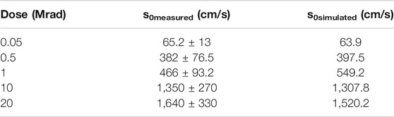
TABLE 6. Measured and simulated surface generation velocity from FBK p-on-n gated-diodes.
Discussion
Surface damage effects induced by radiation have been characterized by means of experimental measurements and TCAD numerical simulations. Extensive measurement campaigns have been performed on gated-diodes, MOS capacitors and MOSFETs fabricated by three principal vendors of solid-state particle detectors, namely Fondazione Bruno Kessler (FBK) in Italy, Hamamatsu Photonics (HPK) in Japan and Infineon Technologies (IFX) in Austria on both n-type and p-type substrates (with and without p-spray implantation layer). From these measurements the relevant parameters which rule the surface damage effects were extrapolated. Indeed, the interface trap density NIT and the oxide charge density QOX, have been determined at each X-ray irradiation step within the range of 0–100 Mrad(SiO2). Acceptor-like and donor-like interface state characteristics have been investigated by exploiting devices fabricated on both polarity substrates. The measurements repeatability and the crosscheck between correspondent parameters obtained from different test structures highlights on the one hand the measures reliability and on the other hand the generality of the parameters for the surface damage modeling purpose.
The values of NIT and QOX, extrapolated from measurements, have been fed as inputs to TCAD simulation tools, aiming at the validation of the “Perugia Surface 2019” physics meaningful TCAD numerical model for the surface radiation damage characterization. The validation relies on the comparison between simulation results and experimental data in terms of C-V characteristics of n-type MOS capacitors, p-type MOS capacitors with p-spray and I-V curves of both p-on-n and n-on-p gated-diodes as a function of the dose. The good agreement obtained for all the tested devices and for all the considered irradiation doses qualifies the validity of the pursued method and the comprehensiveness of the selected relevant parameters. As an example, a significant figure of merit of irradiated device was the surface generation velocity of gated-diode, which has been very well reproduces, even at higher doses.
The robustness of the developed modeling scheme and its versatility has been further proved with the simulation of p-type MOS capacitors with p-spray layer. Although the presence of the p-spray further complicates the investigation of the interplay between interface trap states and fixed oxide charge build-up at the SiO2/Si interface, the developed modeling scheme reveals to be suitable for the reproduction of the C-V electrical behavior.
For each considered technology option, an analytical model has been developed in order to describe the build-up of the fixed oxide charge and the rise of the trap density as a function of the imparted X-ray dose, providing values for the radiation related parameters even at different doses from the experimentally investigated ones.
When numerical simulations are capable of verify experimental results, they will also gain predictive power, resulting in reduced time and cost in detector design and testing. Indeed, the new developed numerical surface radiation damage model, fully implemented within the TCAD environment, can be proficiently applied for predictive insight of the detectors’ electrical behavior. Not only different design options/detector geometries can be evaluated, but also different vendors and/or technology options can be investigated, aiming at the performance optimization of the new generation of silicon detectors to be used in the future HL-LHC scenario.
Data Availability Statement
The original contributions presented in the study are included in the article/Supplementary Material, further inquiries can be directed to the corresponding author.
Author Contributions
AM and FM devised the “Perugia 2019 Surface” damage modeling scheme. AM performed the simulations, the data analysis and wrote the paper. FM performed all the measurements on the different test structures. FM and DP contributed to the writing of this paper. TC contributed to the simulation implementation. DP contributed to the data analysis.
Funding
This project has received funding from the European Union’s Horizon 2020 Research and Innovation program with the project AIDA-2020 under Grant Agreement no. 654168 and PRIN Project 2017 2017L2XKTJ 4DInSiDe.
Conflict of Interest
The authors declare that the research was conducted in the absence of any commercial or financial relationships that could be construed as a potential conflict of interest.
Acknowledgments
The authors gratefully acknowledge Serena Mattiazzo for the support during the irradiation phases at the SIRAD irradiation facility in Legnaro (PD), Italy and the INFN (ATLAS-CMS)-FBK “phase 2” collaboration for providing the FBK test structures.
Supplementary Material
The Supplementary Material for this article can be found online at: https://www.frontiersin.org/articles/10.3389/fphy.2021.617322/full#supplementary-material.
References
1. Unno Y, Ikegami Y, Kohriki T, Terada S, Hara K, Yamamura K, et al. Optimization of surface structures in n-in-p silicon sensors using TCAD simulation. Nucl Instrum Methods Phys Res A (2011) 636:S118–S124. doi:10.1016/j.nima.2010.04.095
2. Pennicard D, Pellegrini G, Fleta C, Bates R, O’Shea V, Parkes C, et al. Simulations of radiation-damaged 3D detectors for the Super-LHC. Nucl Instrum Methods A (2008) 592:16. doi:10L8.03.100
3. Barbottin G, Vapaille A. New insulators, devices and radiation effects. 1st Edn, 3. Amsterdam, Netherlands: Elsevier (1999).
4. Chang ST, Wu JK, Lyon SA Amphoteric defects at the Si-SiO2 interface. Appl Phys Lett (1986) 48:662. doi:10.1063/1.96736
5. Nicollian EH, Brews JR. MOS (metal oxide semiconductor) physics and technology. Hoboken, NY: John Wiley and Sons (1982). p. 319–356.
6. McWhorter PJ, Winokur PS Simple technique for separating the effects of interface traps and trapped-oxide charge in metal-oxidesemiconductor transistors. Appl Phys Lett (1986) 48:133. doi:10.1063/1.96974
7. Moscatelli F, Passeri D, Morozzi A, Mattiazzo S, Dalla Betta G-F, Bilei GM Effects of interface donor trap states on isolation properties of detectors operating at high-luminosity LHC. IEEE Trans Nucl Sci (2017) 64(Issue 8). 2259–2287. doi:10.1109/TNS.2017.2709815
8. Bisello D, Candelori A, Kaminski A, Litovchenko A, Noah E, Stefanutti L X-ray radiation source for total dose radiation studies. Radiat Phys Chem (2004) 71:713–5. doi:10.1016/j.radphyschem.2004.04.071
9. Morozzi A, Moscatelli F, Passeri D, Bieli GM TCAD advanced radiation damage modeling in silicon detectors. In: Proceedings of the 28th international workshop on vertex detectors (Vertex 2019); 2019 October; Lopud Island, Croatia (2019). p. 2020.
10. Moscatelli F, Morozzi A, Passeri D, Mattiazzo S, Dalla Betta G-F, Bergauer T, et al. Analysis of surface radiation damage effects at HL-LHC fluences:comparison of different technology options. Nucl Instrum Methods Phys Res A (2019) 924:198–202. doi:10.1016/j.nima.2018.07.081
11. Morozzi A, Moscatelli F, Lombardi G, Bilei GM, Hinger V, Bergauer T, et al. Characterization of irradiated p-type silicon detectors for TCAD surface radiation damage model validation. J Inst Met (2020) 15:C01029. doi:10.1088/1748-0221/15/01/C01029
12. Moscatelli F, Passeri D, Morozzi A, Dalla Betta G-F, Mattiazzo S, Bomben M Surface damage characterization of FBK devices for high luminosity LHC (HL-LHC) operations. J Inst Met (2017) 12:P12010. doi:10.1088/1748-0221/12/12/P12010
13. Mariani V, Moscatelli F, Morozzi A, Passeri D, Mattiazzo S, Bergauer T, et al. On behalf of the CMS collaboration, measurements of surface and bulk radiation damage effects in silicondetectors for phase-2 CMS outer tracker. Nucl Instrum Methods Phys Res A (2020) 980:164423. doi:10.1016/j.nima.2020.164423
14. Moscatelli F, Morozzi A, Passeri D, Mattiazzo S, Dalla Betta G-F, Bergauer T, et al. Measurements and simulations of surface radiation damage effects on IFXand HPK test structures. Nucl Instrum Methods Phys Res A (2020) 958:162794. doi:10.1016/j.nima.2019.162794
15. Fleetwood DM, Winokur PS, Reber RA, Meisenheimer TL, Schwank JR, Shaneyfelt MR, et al. Effects of oxide traps, interface traps, and border traps on metal-oxide -semiconductor devices. J Appl Phys. (1993) 73:5058–5074. doi:10.1063/1.353777
16. Verzellesi G, Dalla Betta GF, Bosisio L, Boscardin M, Pignatel GU, Soncini G On the accuracy of generation lifetime measurement in high-resistivity silicon using PN gated-diodes. IEEE Trans Electron Dev. (1999) 46(4):817–820. doi:10.1109/16.753724
17. Peltola T Simulation of radiation-induced defects. In: Proceedings of the 24th International Workshop on Vertex Detectors (VERTEX2015); 2015 June; Santa Fe, NM (2015):31. doi:10.22323/1.254.0031
18. Dalal R, Bhardwaj A, Ranjan K, Moll M, Elliott-Peisert A Combined effect of bulk and surface damage on strip insulation properties of proton irradiated n+-p silicon strip sensors. J Inst Met (2014) 9:P04007. doi:10.1088/1748-0221/9/04/P04007
19. Moll M Displacement damage in silicon detectors for high energy physics. IEEE Trans Nucl Science (2018) 65(8):1561–82. doi:10.1109/TNS.2018.2819506
20. Zhang J, Fretwurst E, Klanner R, Pintilie I, Schwandt J, Turcato M Investigation of X-ray induced radiation damage at the Si-SiO2 European XFEL. J Inst Met (2012) 7:C12012. doi:10.1088/1748-0221/7/12/C12012
21. Schwandt J. Design of a radiation hard silicon pixel sensor for X-ray science. Ph.D. dissertation. Hamburg (Germany): Universität Hamburg (2014).
22. Schwandt J, Fretwurst E, Klanner R, Pintilie I, Zhang J Optimization of the radiation hardness of silicon pixel sensors for high X-ray doses using TCAD simulations. J Instrum (2012) 7:C01006. doi:10.1088/1748-0221/7/01/C01006
23. Moscatelli F, Passeri D, Morozzi A, Mattiazzo S, Dalla Betta G-F, Dragicevic M, et al. Radiation damage effects on p-type silicon detectors for high-luminosity operations: test and modeling. In: Proceedings of the 16th European conference on radiation and its effects on components and systems. RADECS; 2016 September; Bremen, Germany (2016). doi:10.1109/RADECS.2016.8093111
24. Morozzi A, Passeri D, Moscatelli F, Dalla Bettad G-F, Bilei GM A combined surface and bulk TCAD damage model for the analysis of radiation detectors operating at HL-LHC fluences. J Inst Met (2016) 11:C12028. doi:10.1088/1748-0221/11/12/C12028
25. Moscatelli F, Passeri D, Morozzi A, Mendicino R, Dalla Betta G-F, Bilei GM Combined bulk and surface radiation damage effects at very high fluences in silicon detectors: measurements and TCAD simulations. IEEE Trans Nucl Sci (2016) 63(5):2716–2723. doi:10.1109/TNS.2016.2599560
26. Morozzi A, Passeri D, Moscatelli F, Lombardi G, Bilei GM, TCAD sensitivity analyses of the university of Perugia surface radiation damage model. In: IEEE nuclear science symposium and medical imaging conference proceedings (NSS/MIC); 2018 November; Sydney, Australia (2018). doi:10.1109/NSSMIC.2018.8824353
27. Zhang J, Fretwurst E, Klanner R, Perrey H, Pintili I, Poehlsen T, et al. Study of X-ray radiation damage in silicon sensors. J Instum (2011) 6:C11013. doi:10.1088/1748-0221/6/11/C11013
28. Zhang J, Pintilie I, Fretwurst E, Klanner R, Perrey H, Schwandt J Study of radiation damage induced by 12 keV X-rays in MOS structures built on high-resistivity n-type silicon. J Synchrotron Radiat (2012) 19:340–6. doi:10.1107/S0909049512002348
Keywords: radiation damage, silicon detectors, solid-states detectors, TCAD simulations, radiation hardness
Citation: Morozzi A, Moscatelli F, Croci T and Passeri D (2021) TCAD Modeling of Surface Radiation Damage Effects: A State-Of-The-Art Review. Front. Phys. 9:617322. doi: 10.3389/fphy.2021.617322
Received: 14 October 2020; Accepted: 04 January 2021;
Published: 02 February 2021.
Edited by:
Angela Kok, Sintef Digital, NorwayReviewed by:
Marco Mandurrino, National Institute of Nuclear Physics of Turin, ItalyGabriele Giacomini, Brookhaven National Laboratory (DOE), United States
Copyright © 2021 Morozzi, Moscatelli, Croci and Passeri. This is an open-access article distributed under the terms of the Creative Commons Attribution License (CC BY). The use, distribution or reproduction in other forums is permitted, provided the original author(s) and the copyright owner(s) are credited and that the original publication in this journal is cited, in accordance with accepted academic practice. No use, distribution or reproduction is permitted which does not comply with these terms.
*Correspondence: Arianna Morozzi, arianna.morozzi@pg.infn.it