
Abstract
We demonstrate that the critical thickness for Ge-rich strained SiGe layers can be drastically increased by a factor of more then two by means of growth on mesa-patterned Ge-on-Si. The Si0.2Ge0.8 layer grown on sub-millimeter mesa Ge-on-Si is fully strained and free from ridge roughness, while the same Si0.2Ge0.8 layers grown on unpatterned Ge-on-Si and a Ge substrate are partially strain-relaxed with the surface covered by high-density ridge roughness. This demonstrates that the proposed patterning method can provide thick and stable strained SiGe films as promising templates for realization of strained SiGe-based optoelectronic and spintronic devices.
Export citation and abstract BibTeX RIS

Content from this work may be used under the terms of the Creative Commons Attribution 4.0 license. Any further distribution of this work must maintain attribution to the author(s) and the title of the work, journal citation and DOI.
Strain engineering technologies based on Si/Ge heterostructures have been intensively researched for decades for various device applications. 1) A number of studies have focused on Si/Ge heterostructures on Si substrates, meaning that Si-rich SiGe alloy materials have been major targets. In contrast, Ge-rich strained Si/Ge heterostructures are also highly attractive for various applications such as high-mobility channels for metal–oxide–semiconductor field-effect transistors (MOSFETs) and photonic devices. 2–9) It is generally difficult, however, to grow high-quality Ge-rich SiGe alloys on Si due to the large lattice mismatch. By replacing the Si substrate with Ge, it can be easier to grow high-quality Ge-rich SiGe, but the fact that the bulk Ge wafer is still costly and not appropriate for mass production has prevented intensive research so far.
Recently, however, techniques to fabricate Ge virtual substrates directly on a Si substrate have been developed based on a so-called two-step growth method, 10–19) and the crystal quality of the epitaxial Ge layer on Si (Ge-on-Si) has been significantly improved, allowing us to explore the strain engineering of Ge-rich Si/Ge heterostructures on Ge-on-Si. 20,21) However, there are still few reports, particularly on strain stabilities, relaxation behaviors and critical thickness for tensile-strained SiGe films grown on the Ge.
In terms of surface orientations, an orientation of (111) for Ge is very attractive since higher electron mobility can be obtained in Ge(111) channels than in Ge(100) channels. 22,23) Moreover, high-quality ferromagnetic materials can be epitaxially grown on Ge(111) and Ge-rich SiGe(111), 24–29) allowing us to realize Ge or SiGe channel spintronics devices. Recently, pure spin-current transport has been demonstrated in a SiGe(111) channel layer. 29) Moreover, since the spin relaxation mechanism is related to the L-valley structures of the conduction band in Ge and SiGe, introduction of strain into the SiGe(111) channel is expected to improve the spin lifetime through valley splitting. 29)
In this context, therefore, it can be said that the strain engineering of SiGe/Ge heterostructures with a (111) surface orientation based on Ge-on-Si(111) is of great importance for various applications such as n-type MOSFETs as well as spintronic devices. Recently, we have systematically investigated the initial stages of strain relaxation behavior of strained SiGe on Ge, 30,31) where it has been shown that the formation of cracks and accompanying surface ridge roughness reflects the commencement of the relaxation and that the critical thickness of SiGe on Ge-on-Si(111) is much lower than that on a Ge(111) substrate, which strongly demands new approaches to improve the reduced critical thickness.
To this end, we attempted to grow strained SiGe on patterned Ge-on-Si(111) and succeeded in effective suppression of the crack formation accompanying the strain relaxation, where the pattern width is comparable to the crack spacing, i.e. several micrometers. 30) Thus, we speculated that the pattern edges, instead of the cracks, can reduce the strain energy accommodated in the strained SiGe layer, and as a result prevent the cracks from arising in the SiGe film. For integration of a number of devices, however, strained SiGe layers with much larger areas are required.
In this study, we aim to grow the strained SiGe on much larger, up to sub-millimeter scale, mesa-patterned Ge-on-Si(111). We demonstrate that such a large mesa has drastic effects on suppression of crack formation; as a result, the critical thickness of SiGe on the patterned Ge-on-Si(111) is significantly enhanced far beyond that on unpatterned Ge(111) substrates.
The crystal growth of Si/Ge heterostructures was carried out using solid source molecular beam epitaxy. The Ge-on-Si(111) was fabricated using the so-called two-step growth method. 12–21) The 40 and 650 nm thick Ge layers were successively grown on a 3 inch Si(111) wafer at growth temperatures of 400 and 750 °C, respectively, followed by post-annealing at 800 °C for 10 min. Subsequently, the patterning of the Ge-on-Si layer was performed by the standard photolithographic process, with rectangle-shaped mesa patterns being defined. Outside of the mesa pattern, the Ge layer was completely etched down with the selective etchant H2O2 that does not etch the Si substrate. The rectangle sizes were varied from 80 μm × 80 μm to 200 μm × 600 μm. More than 100 mesa patterns with various sizes were continuously arrayed at intervals of around 50 μm to 150 μm over the roughly 3 mm × 3 mm square chip.
On the patterned Ge-on-Si, strained Si1–x Gex (x = 0.80) layers with thicknesses of 160, 200 and 250 nm were grown at 350 °C. For comparison, the strained SiGe layers were simultaneously grown on unpatterned Ge-on-Si and Ge(111) substrates. Surface morphologies were evaluated with a laser microscope (LM). Local strain states were evaluated by micro-Raman measurement, where a 532 nm laser with a beam spot of 1 μm2 was incident on a selected point of the sample surface. Also, crystallinities and relaxation ratios were characterized by X-ray diffraction (XRD) reciprocal space mapping measurements.
Figure 1 shows LM images of Si0.20Ge0.80 layers with thicknesses of (a)–(c) 160 nm, (d)–(f) 200 nm and (g)–(i) 250 nm grown on unpatterned Ge(111) substrates (a, d, g), unpatterned Ge-on-Si(111) (b, e, h) and rectangle-shaped mesa-patterned Ge-on-Si(111) (c, f, i). Line-shaped ridges clearly appear on the surfaces of the SiGe layers on both the unpatterned Ge-on-Si and Ge substrates. It is clearly found that the densities of the ridges on the unpatterned Ge-on-Si are much higher than those on the Ge substrates. For the patterned SiGe layers, on the other hand, the surfaces are free from the ridges except for one area in Fig. 1(i).

Fig. 1. (Color online) Laser microscope surface images of the 160, 200 and 250 nm thick strained Si0.2Ge0.8 layers grown on (a), (d), (g) unpatterned Ge(111), (b), (e), (h) unpatterned Ge-on-Si(111) and (c), (f), (i) the patterned Ge-on-Si(111) substrate, respectively.
Download figure:
Standard image High-resolution imageAs the thickness of the SiGe layers increases, the ridge densities are seen to gradually increase, which implies that the strain relaxation is proceeding with the increase in thickness. As we studied in a previous work, 31) for many thinner SiGe layers the critical thickness, beyond which the ridges appear, for SiGe on a Ge-on-Si and a Ge substrate were as thin as 70 and 100 nm, respectively. In this work, although the thickness of the strained SiGe significantly exceeds the critical thickness, ridges are hardly observed up to 200 nm for the patterned samples. It was confirmed that all mesa patterns on the chips were free from the ridges. From this result, it can be said that the critical thickness is beyond 200 nm when SiGe is grown on mesa-patterned Ge-on-Si.
For the 250 nm sample, interestingly we find that most of the mesas are free from the ridges while some mesas are found to be covered by high-density ridges. As shown below, the ridge-free SiGe on the mesa is fully strained without any strain relaxation. The number of ridge-free mesas is over 85% of the total number of mesas, which means that the generation of ridges commences around this thickness. Therefore, we can say that the critical thickness is roughly 200–250 nm when patterning is performed. This critical thickness is more than twice the critical thickness of SiGe on a Ge substrate.
Concerning generation of the ridges and their effective suppression through patterning, we propose the following possible mechanisms. First, the ridge roughness appears following crack generation due to local accumulation of migrating Si/Ge adatoms around the crack edges. 30) Punctate defects on the Ge surface for both the Ge substrate and Ge-on-Si are possible sources of crack generation, and provided that several punctate defects exist closely with each other, cracks are generated connecting such defects. Once an initial crack is generated in the SiGe film, a network of cracks is considered to spread very fast over the SiGe film. The patterning can effectively separate such defects into different mesa patterns, resulting in extinction of the driving force for crack generation. Note that under the current variation of pattern sizes we cannot observe a clear pattern size dependence of the crack generation behavior. Pattern size and density dependences are under investigation to demonstrate this mechanism.
Averaged line densities estimated from these LM images are plotted in Fig. 2, where the average spacing of the ridges, defined as an inverse of the density, is also shown. The density can be seen to increase monotonically with thickness and the densities for SiGe on Ge-on-Si are about twice that on Ge substrates for thicknesses of 200 and 250 nm. For the patterned sample, the ridge density is constantly zero except for a small number of mesas for the 250 nm thick sample. The ridge density on the mesa is coincident with that of SiGe on unpatterned Ge-on-Si. We speculate that a source of crack generation existed on the mesa and once the crack has generated from the source the cracks multiply very quickly and the density approaches that of the unpatterned sample. Detailed investigations are now under way.
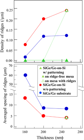
Fig. 2. (Color online) Density of ridges and average spacing of ridges for 160, 200 and 250 nm thick Si0.2Ge0.8 on patterned Ge-on-Si(111), unpatterned Ge-on-Si(111) and Ge(111) substrates, respectively.
Download figure:
Standard image High-resolution imageStrain states were evaluated by Raman measurements for the samples with 250 nm thick SiGe layers grown on Ge-on-Si with and without patterning. For the patterned sample, a Raman laser beam spot was focused on the area inside or outside the mesa, and spectra from both areas were individually obtained. The mesa free from the ridges was chosen for this measurement. For the unpatterned sample, the laser spot was focused just on the surface-ridged point or the flat area between the ridges.
Figure 3(a) shows the obtained Raman spectra. We can find Ge–Ge and Si–Ge mode peaks around 280 and 400 cm−1, respectively, for all spectra whereas peak values differ slightly, meaning that the strain states are different. It is known that peak shifts to higher wavenumbers correspond to partial relaxation of the originally induced tensile strain. The largest shift, that is the largest strain relaxation, is observed for the SiGe outside the mesa, where the Ge-on-Si is completely etched and the SiGe layer is grown directly on the Si substrate. The lattice mismatch between Si0.2Ge0.8 and Si is so large that the SiGe layer is immediately strain-relaxed. Also, the SiGe on the surface-ridged point reveals that the large strain relaxation takes place locally, which was observed and discussed in Ref. 31. In contrast, the SiGe on the mesa and the SiGe between the ridges exhibit lower wavenumbers, implying that the tensile strain is well maintained. Degrees of relaxation can be quantitatively analyzed by XRD measurements (see below). It is noticeable that the peak from the SiGe between the ridges is seen to shift slightly compared with the SiGe on the mesa, as shown in the inset zoomed view of the peaks. From these results, it can be concluded that the SiGe on the mesa of the patterned Ge-on-Si is the most stable against strain relaxation.

Fig. 3. (Color online) (a) Raman spectra inside and outside the mesa for 250 nm thick Si0.2Ge0.8 on the patterned Ge-on-Si(111) substrate and between and on the ridges for 250 nm Si0.2Ge0.8 on the unpatterned Ge-on-Si(111) substrate, respectively. XRD reciprocal space mapping images of Si0.2Ge0.8 layers (b) on the patterned Ge-on-Si(111) and (c) the unpatterned Ge-on-Si, respectively.
Download figure:
Standard image High-resolution imageFigures 3(b) and 3(c) show XRD reciprocal space mapping (RSM) images of the 250 nm thick SiGe layers on the patterned and unpatterned Ge-on-Si(111), respectively. The spot size of the X-ray incident beam is of the order of several millimeters so that a number of mesa patterns as well as areas outside the mesa patterns are included in the diffracted X-ray signal, meaning that the strain states of the SiGe layer both inside and outside the mesa pattern can be evaluated simultaneously from the XRD RSM. For both images, in addition to a strong peak of the Si substrate around a reciprocal lattice unit Qx of 0.521 Å−1, two main peaks coming from the SiGe and Ge-on-Si layers are clearly observed. In the case of the sample with mesa patterning [Fig. 3(b)], the signal from the SiGe can be separated into two components. One is a sharp one at a Qx of 0.499 Å−1 and another is a broad one roughly from 0.499 Å−1 to 0.509 Å−1. By comparison with the Raman results above, we can estimate that the former and the latter should come from the SiGe inside and outside the mesa pattern, respectively, since the SiGe inside and outside the mesa has been verified to be strained and relaxed, respectively. The sharp peak from the SiGe inside the mesa is located at the same Qx as that of the underlying Ge-on-Si, which means that the SiGe on the mesa is fully strained on the Ge-on-Si without any partial strain relaxation. Another broad peak from the SiGe outside the mesa reveals that the SiGe is almost fully relaxed, which is consistent with the Raman results above.
By contrast, in the case of the unpatterned sample [Fig. 3(c)], the SiGe peak is broadened and the center peak Qx and Qz values slightly shift to higher and lower values, respectively, compared with the peaks of the patterned sample [Fig. 3(b)]. These peak shifts mean that a small strain relaxation occurs for the unpatterned sample, and the estimated relaxation ratio is approximately 22%. The Raman results show that strain relaxation occurs locally around the ridged roughness. The broadening of the SiGe peak is thus considered to be caused by the non-uniform strain relaxation of the SiGe layer on the unpatterned Ge-on-Si. It is interesting to note that the peak of Ge-on-Si is significantly modified after the growth of SiGe. An original peak before SiGe growth (not shown here) was very sharp and almost the same as the peak observed for the patterned sample. It has been shown that the cracks generated in the SiGe layer extend into the underlying Ge layer. 30) We can consider that the tensile strain originally induced in the Ge-on-Si is highly relaxed due to crack formation in the Ge-on-Si layer; additionally, the shear stress provided by the overgrown SiGe affects the crystallinity, resulting in asymmetric broadening of the peak. This phenomenon is also completely avoided in the patterned sample.
For comparison, thicknesses of the above-discussed three patterned samples are plotted in a graph of critical thickness versus misfit strain (Fig. 4), where theoretically and experimentally reported curves of critical thickness are included. 31,32) Circle plots correspond to the samples which did not exhibit strain relaxation in all mesa patterns. A triangle plot corresponds to the sample which shows partial surface ridges on less than 15% of mesa patterns and does not show strain relaxation on more than 85% mesa patterns, as seen in Fig. 1(i). Hence the assumed critical thickness lies between 250 and 200 nm in the case of patterning.

Fig. 4. (Color online) SiGe critical thickness against misfit strain. Thicknesses of the SiGe grown on patterned Ge-on-Si in this study are plotted.
Download figure:
Standard image High-resolution image
The dashed line in Fig. 4 represents metastable critical thickness for SiGe on Si(100), 32) which can be compared with this work because the SiGe growth here was carried out at a relatively low temperature, that is under metastable conditions. Solid lines represent the critical thickness for SiGe on unpatterned Ge-on-Si(111), Ge(111) and Ge(100) substrates, which were experimentally obtained in our previous work. 31) It is remarkable that the critical thickness derived in this work is far in excess of all these curves, obviously demonstrating a significant effect of the patterning for increasing the critical thickness.
In conclusion, we studied surface morphologies and strain states for Ge-rich strained SiGe layers grown on patterned and unpatterned Ge-on-Si(111) and a Ge(111) substrate, and demonstrated that the patterning can drastically suppress the strain relaxation involved in crack formation in the SiGe films. The critical thickness was markedly increased beyond 200 nm, while it is around 100 nm without the patterning. It is additionally noted that the mesa patterning size here is as large as several hundred micrometers to sub-millimeter size which is highly applicable to device integration. We can say that sufficiently thick tensile-strained SiGe formed on the mesa Ge-on-Si can provide very promising platforms for strain-engineered Ge-rich Si/Ge heterostructure-based high-performance MOSFETs, photonics and spintronic devices.
Acknowledgments
This work was supported in part by Grant-in-Aid for Scientific Research (Nos 19H02175, 19H05616 and 20K21009) from MEXT, Japan.