3D Photon-To-Digital Converter for Radiation Instrumentation: Motivation and Future Works

 , , , ,
  , ,
, ,  and
and 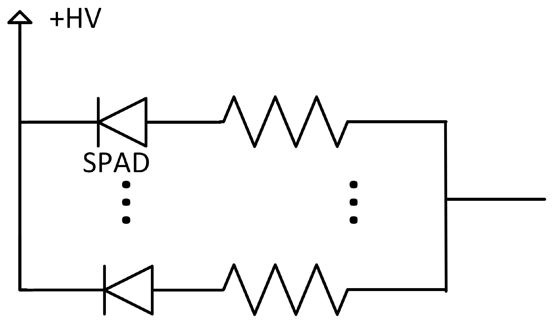
Abstract
:1. Introduction
2. SPAD, Analog SiPM and PDC
Historical Review of SPAD-Based Photodetector
3. Analog versus Digital SPAD Array
3.1. Paradigm Shift or Back to the Start?
3.2. Reading Out Each SPAD Individually
3.3. Power Consumption Comparison
4. 2D versus 3D Integrated PDC
5. Review of 3D PDC
5.1. MIT Lincoln Laboratory
5.2. Hamamatsu Photonics K.K.
5.3. DESY and Semiconductor Laboratory of the Max-Planck-Society (MPG-HLL)
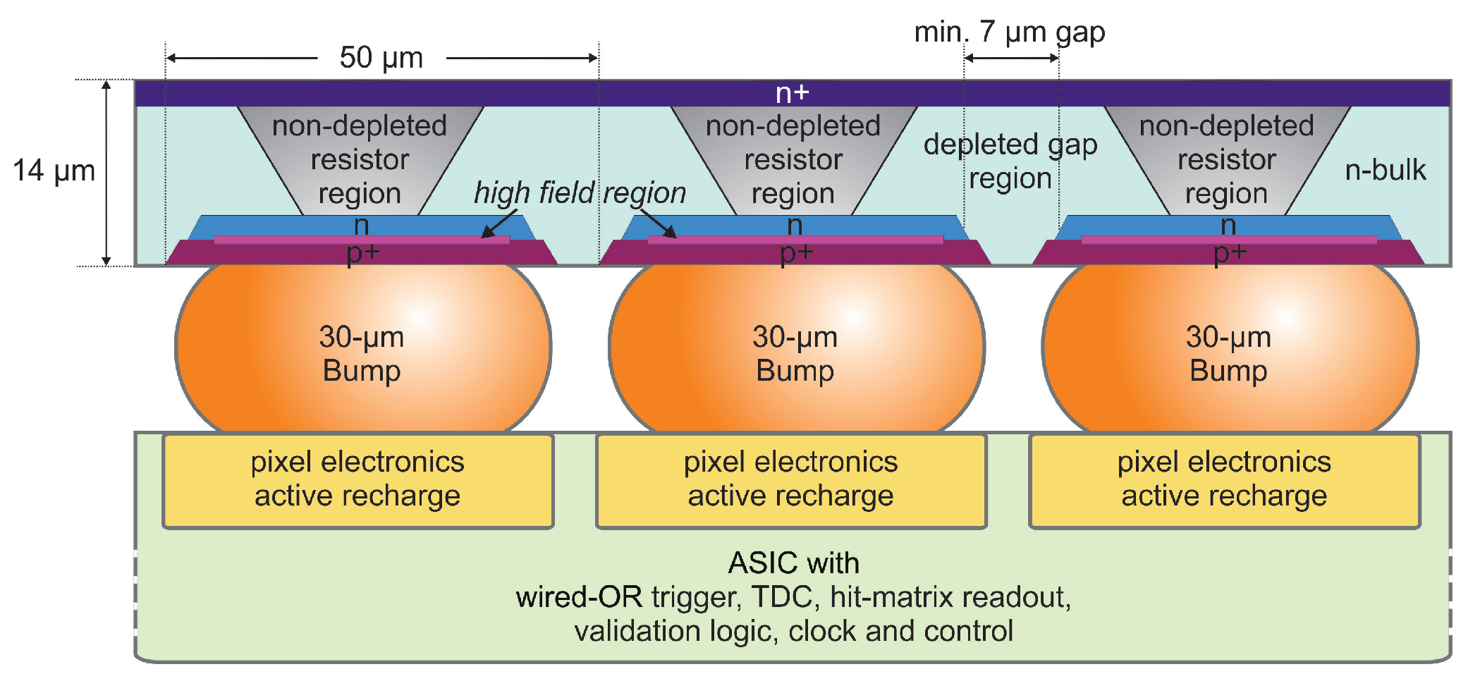
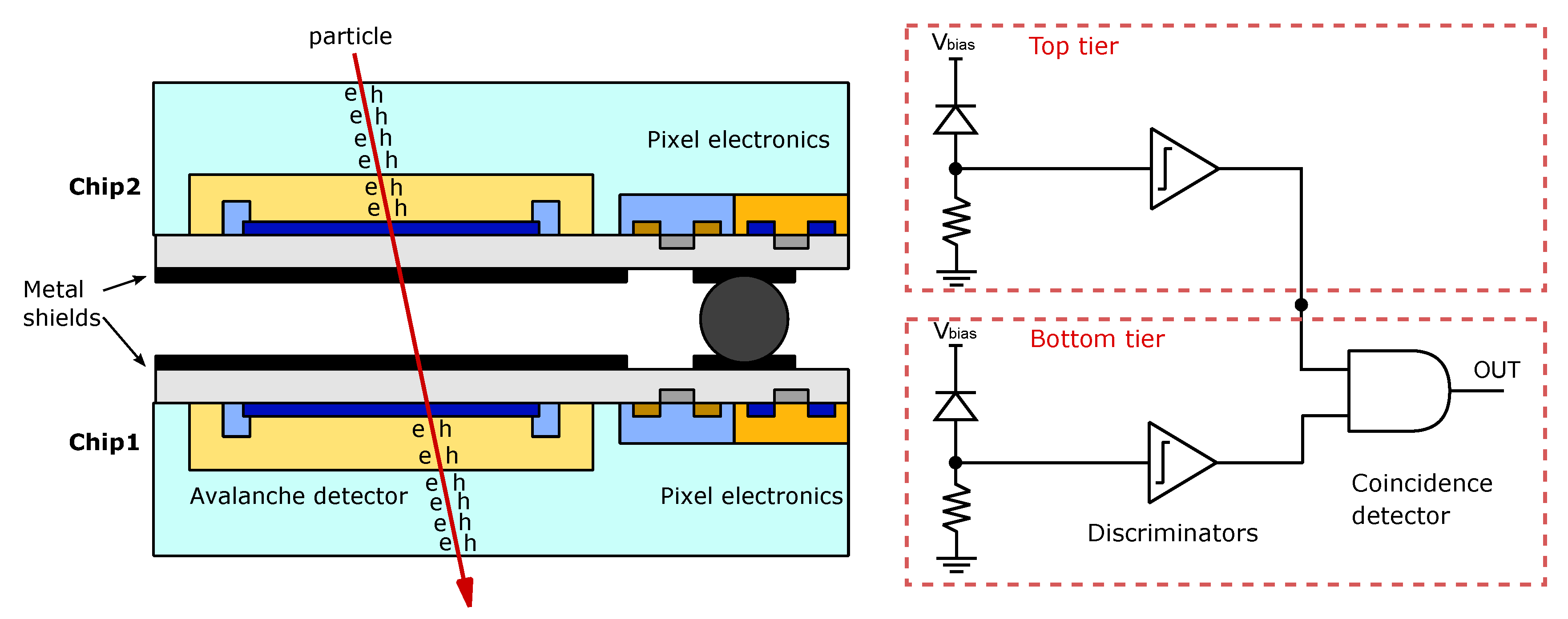
5.4. Istituto Nazionale di Fisica Nucleare (INFN)
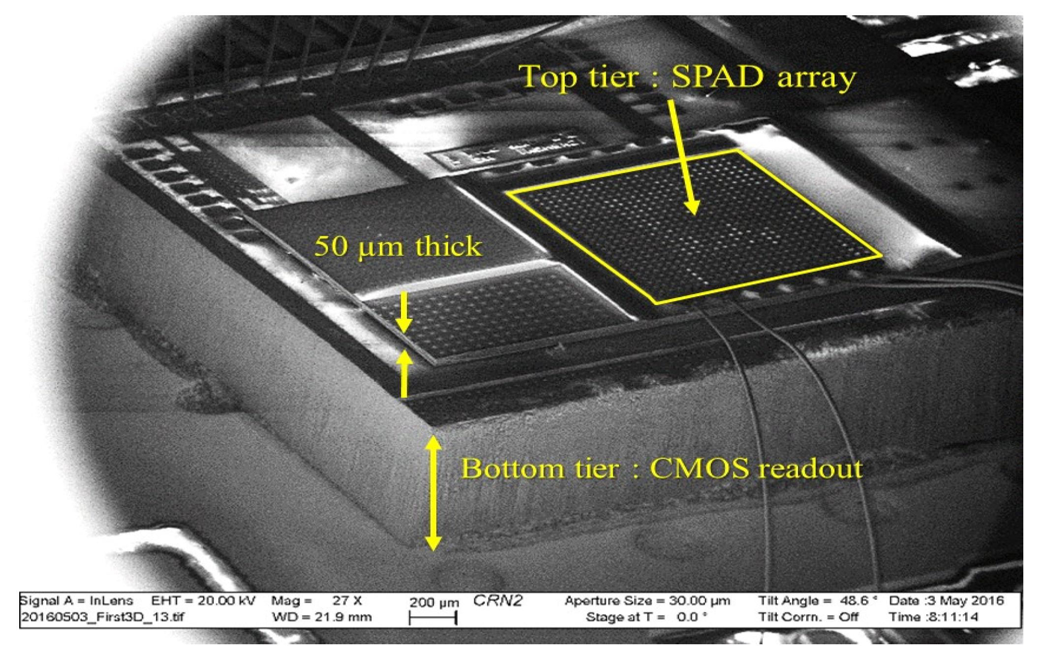
5.5. École Polytechnique Fédérale de Lausanne (EPFL) and TU Delft
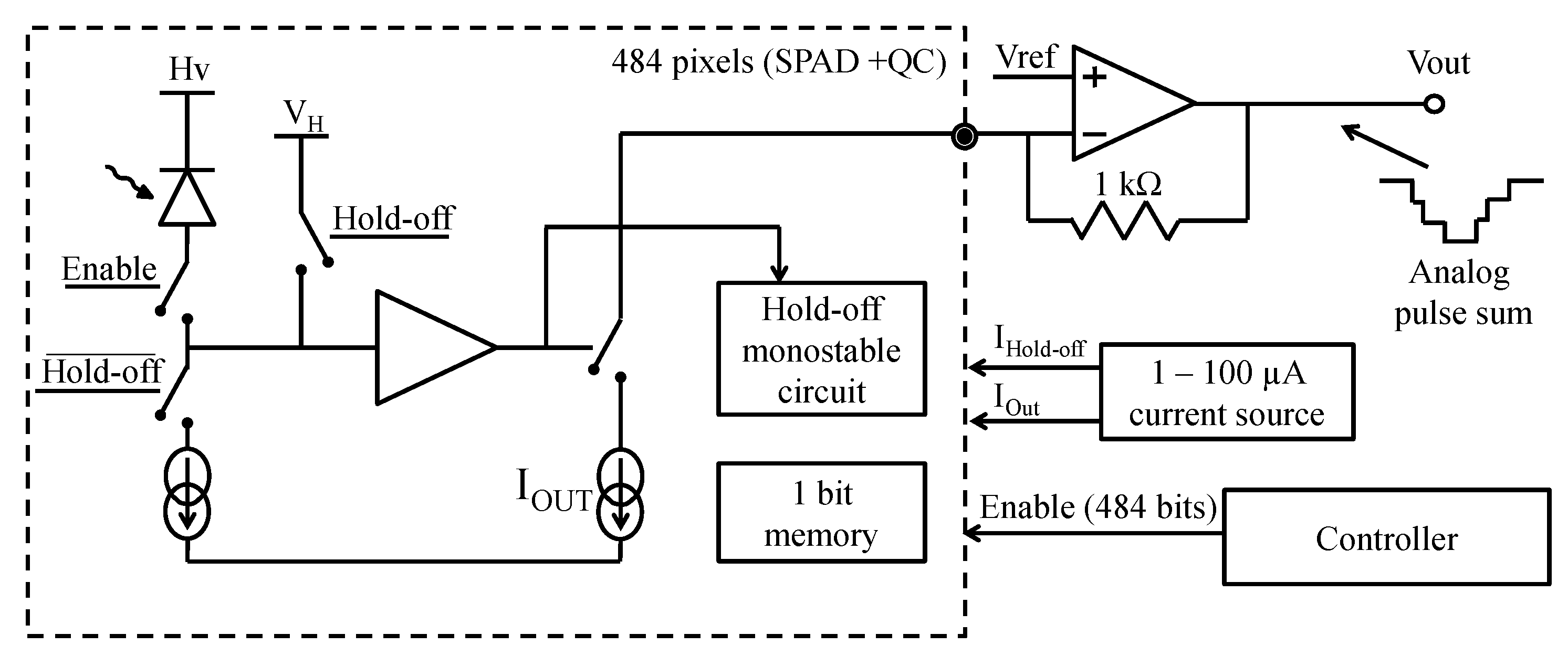
5.6. University of Edinburgh
5.7. Université de Sherbrooke
6. Perspective of 3D PDC for Radiation Instrumentation
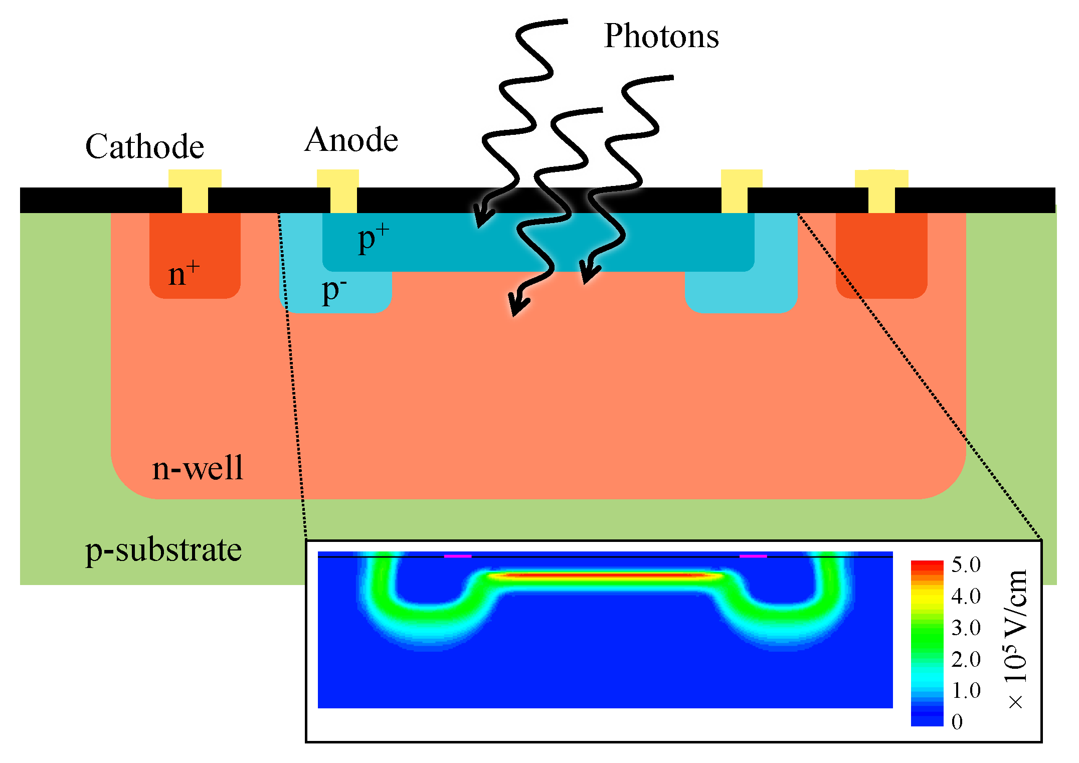
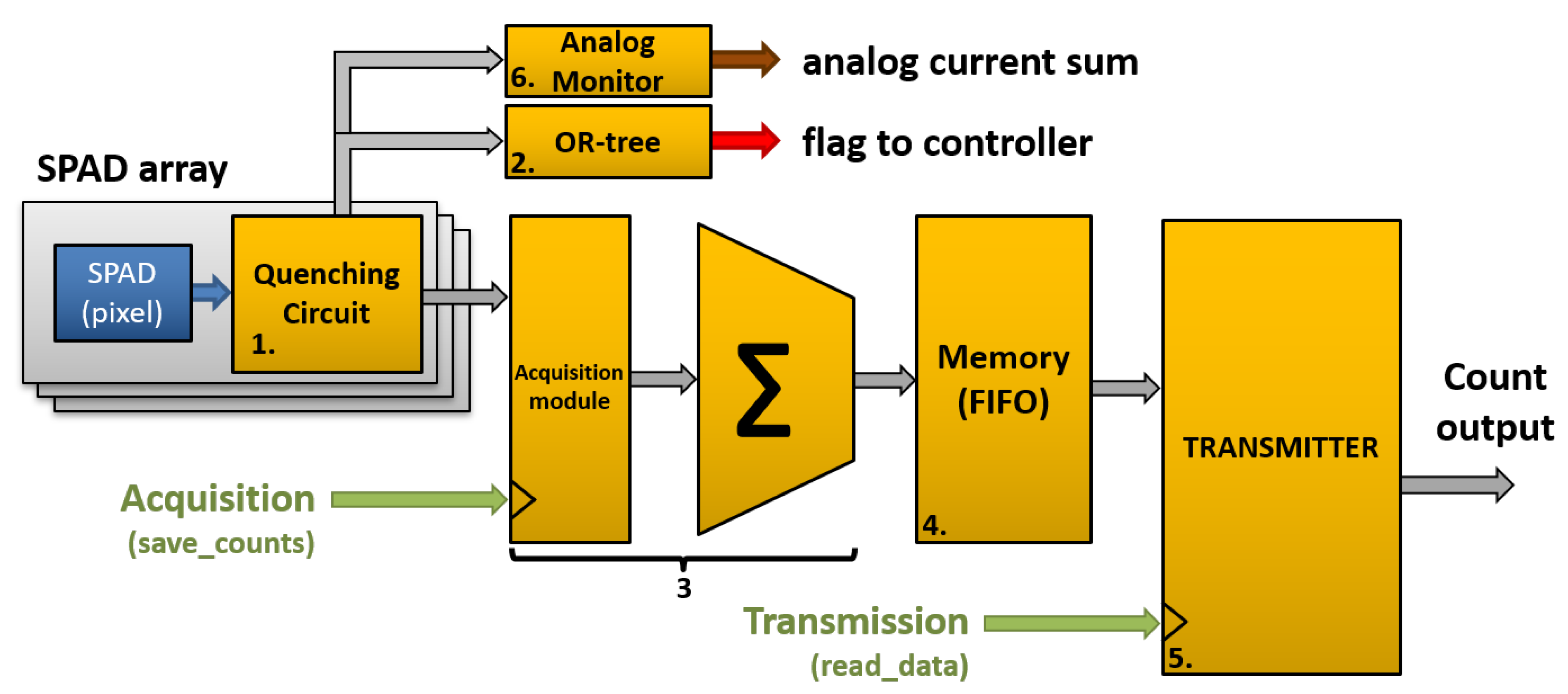
6.1. SPAD Array
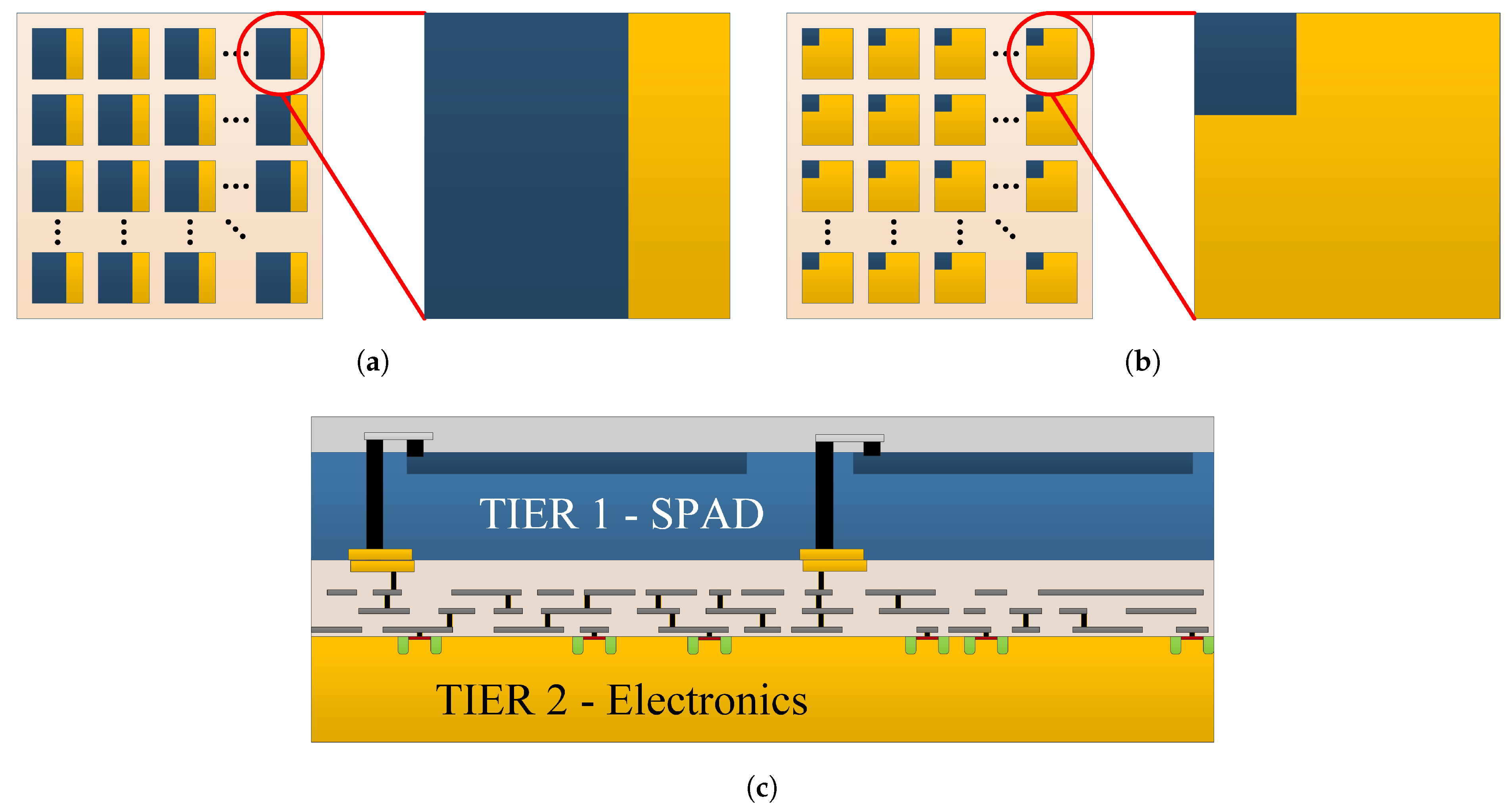
6.2. 3D Vertical Integration
6.3. CMOS Process Choice
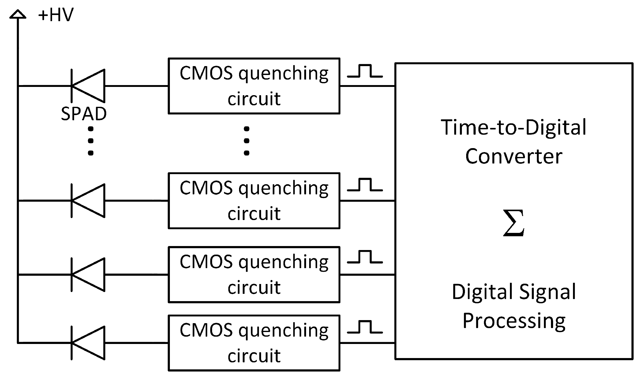
6.4. Quenching Circuit
6.5. Time-to-Digital Converter
6.6. Digital Signal Processing
6.6.1. Time-of-Flight PET Scanner
6.6.2. Liquid Argon and Liquid Xenon Experiments
6.7. 4-Side Tileable
6.8. Tiles for Large-Scale Detector in Cryogenic Operation
6.9. Implementation Challenges
7. Conclusions and Outlook
Author Contributions
Funding
Acknowledgments
Conflicts of Interest
References
- Klanner, R.; Sauli, F. Silicon photomultipliers: Technology, characterisation and applications. Nucl. Instrum. Methods Phys. Res. Sect. A Accel. Spectrom. Detect. Assoc. Equip. 2019, 926, 1–152. [Google Scholar] [CrossRef]
- Saveliev, V.; Golovin, V. Silicon avalanche photodiodes on the base of metal-resistor-semiconductor (MRS) structures. Nucl. Instrum. Methods Phys. Res. Sect. A Accel. Spectrom. Detect. Assoc. Equip. 2000, 442, 223–229. [Google Scholar] [CrossRef]
- Fiorini, C.; Gola, A.; Zanchi, M.; Longoni, A.; Lechner, P.; Soltau, H.; Strüder, L. Gamma-ray spectroscopy with LaBr: Ce scintillator readout by a silicon drift detector. Nucl. Sci. IEEE Trans. 2006, 53, 2392–2397. [Google Scholar] [CrossRef]
- Cherry, S.R.; Sorenson, J.A.; Phelps, M.E. Physics in Nuclear Medicine e-Book; Elsevier Health Sciences: Amsterdam, The Netherlands, 2012. [Google Scholar]
- Cherenkov, P.A. Visible emission of clean liquids by action of γ radiation. Dokl. Akad. Nauk SSSR 1934, 2, 451. [Google Scholar]
- Fülöp, L.; Biró, T. Cherenkov radiation spectrum. Int. J. Theor. Phys. 1992, 31, 61–74. [Google Scholar] [CrossRef]
- Kwon, S.I.; Gola, A.; Ferri, A.; Piemonte, C.; Cherry, S.R. Bismuth germanate coupled to near ultraviolet silicon photomultipliers for time-of-flight PET. Phys. Med. Biol. 2016, 61, L38. [Google Scholar] [CrossRef] [PubMed] [Green Version]
- The CTA Consortium. Design concepts for the Cherenkov Telescope Array CTA: An advanced facility for ground-based high-energy gamma-ray astronomy. Exp. Astron. 2011, 32, 193–316. [Google Scholar] [CrossRef]
- Kadmensky, S.G. Cherenkov radiation as a serendipitous phenomenon. Phys. Uspekhi 2015, 58, 472–479. [Google Scholar] [CrossRef]
- Aprile, E.; Doke, T. Liquid xenon detectors for particle physics and astrophysics. Rev. Mod. Phys. 2010, 82, 2053. [Google Scholar] [CrossRef] [Green Version]
- Albert, J.; nEXO Collaboration. Sensitivity and discovery potential of nEXO to neutrinoless double beta decay. arXiv 2017, arXiv:1710.05075. [Google Scholar]
- Boulay, M.; DEAP Collaboration. DEAP-3600 Dark Matter Search at SNOLAB; Journal of Physics: Conference Series; IOP Publishing: Munich, Germany, 2012; Volume 375, p. 012027. [Google Scholar]
- Amaudruz, P.A.; Baldwin, M.; Batygov, M.; Beltran, B.; Bina, C.; Bishop, D.; Bonatt, J.; Boorman, G.; Boulay, M.; Broerman, B.; et al. Design and construction of the DEAP-3600 dark matter detector. arXiv 2017, arXiv:1712.01982. [Google Scholar] [CrossRef] [Green Version]
- Aalseth, C.; Abdelhakim, S.; Acerbi, F.; Agnes, P.; Ajaj, R.; Albuquerque, I.; Alexander, T.; Alici, A.; Alton, A.; Amaudruz, P.; et al. Design and construction of a new detector to measure ultra-low radioactive-isotope contamination of argon. J. Instrum. 2020, 15, P02024. [Google Scholar] [CrossRef] [Green Version]
- European Strategy for Particle Physics Preparatory Group. Physics briefing book. arXiv 2019, arXiv:1910.11775. [Google Scholar]
- Simon, F. Silicon photomultipliers in particle and nuclear physics. Nucl. Instrum. Methods Phys. Res. Sect. A Accel. Spectrom. Detect. Assoc. Equip. 2019, 926, 85–100. [Google Scholar] [CrossRef]
- Bruschini, C.; Homulle, H.; Antolovic, I.V.; Burri, S.; Charbon, E. Single-photon avalanche diode imagers in biophotonics: Review and outlook. Light. Sci. Appl. 2019, 8. [Google Scholar] [CrossRef]
- Aull, B.; Loomis, A.; Gregory, J.; Young, D. Geiger-mode avalanche photodiode arrays integrated with CMOS timing circuits. Device research conference digest, 1998. In Proceedings of the 56th Annual, IEEE, Charlottesville, VA, USA, 22–24 June 1998; pp. 58–59. [Google Scholar]
- Aull, B.F.; Loomis, A.H.; Young, D.J.; Heinrichs, R.M.; Felton, B.J.; Daniels, P.J.; Landers, D.J. Geiger-mode avalanche photodiodes for three-dimensional imaging. Linc. Lab. J. 2002, 13, 335–349. [Google Scholar]
- Aull, B. Geiger-mode avalanche photodiode arrays integrated to all-digital CMOS circuits. Sensors 2016, 16, 495. [Google Scholar] [CrossRef]
- Ghioni, M.; Gulinatti, A.; Rech, I.; Zappa, F.; Cova, S. Progress in silicon single-photon avalanche diodes. IEEE J. Sel. Top. Quantum Electron. 2007, 13, 852–862. [Google Scholar] [CrossRef]
- Zappa, F.; Tisa, S.; Tosi, A.; Cova, S. Principles and features of single-photon avalanche diode arrays. Sens. Actuators A Phys. 2007, 140, 103–112. [Google Scholar] [CrossRef]
- Einstein, A. Aeber einen die Erzeugung und Verwandlung des Lichtes betreffenden heuristischen Gesichtspunkt. Ann. Der Phys. 1905, 322, 132–148. [Google Scholar] [CrossRef]
- Ohl, R. Light-Sensitive Electric Device. U.S. Patent 2402662, 25 June 1946. [Google Scholar]
- McKay, K.G.; McAfee, K.B. Electron multiplication in silicon and germanium. Phys. Rev. 1953, 91, 1079–1084. [Google Scholar] [CrossRef]
- Wolff, P.A. Theory of electron multiplication in silicon and germanium. Phys. Rev. 1954, 95, 1415–1420. [Google Scholar] [CrossRef]
- Rose, D.J. Microplasmas in silicon. Phys. Rev. 1957, 105, 413–418. [Google Scholar] [CrossRef]
- McIntyre, R.J. Theory of microplasma instability in silicon. J. Appl. Phys. 1961, 32, 983. [Google Scholar] [CrossRef]
- Johnson, K.M. High-speed photodiode signal enhancement at avalanche breakdown voltage. IEEE Trans. Electron Devices 1965, 12, 55–63. [Google Scholar] [CrossRef]
- McIntyre, R. Recent developments in silicon avalanche photodiodes. Measurement 1985, 3, 146–152. [Google Scholar] [CrossRef]
- Antognetti, P.; Cova, S.; Longoni, A. A study of the operation and performances of an avalanche diode as a single photon detector. In Proceedings of the 2nd Ispra Nuclear Electronics Symposium, Stresa, Italy, 20–23 May 1975. [Google Scholar]
- Tisa, S.; Zappa, F.; Tosi, A.; Cova, S. Electronics for single photon avalanche diode arrays. Sens. Actuators A Phys. 2007, 140, 113–122. [Google Scholar] [CrossRef]
- Dautet, H.; Deschamps, P.; Dion, B.; MacGregor, A.D.; MacSween, D.; McIntyre, R.J.; Trottier, C.; Webb, P.P. Photon counting techniques with silicon avalanche photodiodes. Appl. Opt. 1993, 32, 3894–3900. [Google Scholar] [CrossRef] [Green Version]
- Lacaita, A.; Cova, S.; Samori, C.; Ghioni, M. Performance optimization of active quenching circuits for picosecond timing with single photon avalanche diodes. Rev. Sci. Instrum. 1995, 66, 4289–4295. [Google Scholar] [CrossRef] [Green Version]
- Zappa, P.; Ghioni, M.; Cova, S.; Varisco, L.; Sinnis, B.; Morrison, A.; Mathewson, A. Integrated array of avalanche photodiodes for single-photon counting. In Proceedings of the 27th European Solid-State Device Research Conference, Stuttgart, Germany, 22–24 September 1997; pp. 600–603. [Google Scholar]
- Kindt, W.J.; van Zeijl, H.W. Fabrication of Geiger mode avalanche photodiodes. In Proceedings of the 1997 IEEE Nuclear Science Symposium Conference Record, Albuquerque, NM, USA, 9–15 November 1997; Volume 1, pp. 334–338. [Google Scholar] [CrossRef]
- Kindt, W.; van Zeijl, H. Modelling and fabrication of Geiger mode avalanche photodiodes. IEEE Trans. Nucl. Sci. 1998, 45, 715–719. [Google Scholar] [CrossRef] [Green Version]
- Kindt, W. Geiger Mode Avalanche Photodiode Arrays: For Spatially Resolved Single Photon Counting; Delft University Press: Delft, The Netherlands, 1999. [Google Scholar]
- Rochas, A. Single Photon Avalanche Diodes in CMOS Technology; EPFL: Lausanne, Switzerland, 2003. [Google Scholar]
- Rochas, A.; Gani, M.; Furrer, B.; Besse, P.; Popovic, R.; Ribordy, G.; Gisin, N. Single photon detector fabricated in a complementary metal-oxide-semiconductor high-voltage technology. Rev. Sci. Instrum. 2003, 74, 3263–3270. [Google Scholar] [CrossRef] [Green Version]
- Rochas, A.; Gosch, M.; Serov, A.; Besse, P.A.; Popovic, R.S.; Lasser, T.; Rigler, R. First fully integrated 2-D array of single-photon detectors in standard CMOS technology. IEEE Photonics Technol. Lett. 2003, 15, 963–965. [Google Scholar] [CrossRef] [Green Version]
- Niclass, C.; Rochas, A.; Besse, P.A.; Charbon, E. Design and characterization of a CMOS 3-D image sensor based on single photon avalanche diodes. IEEE J. Solid State Circuits 2005, 40, 1847–1854. [Google Scholar] [CrossRef] [Green Version]
- Schaart, D.R.; Charbon, E.; Frach, T.; Schulz, V. Advances in digital SiPMs and their application in biomedical imaging. Nucl. Instrum. Methods Phys. Res. Sect. A Accel. Spectrom. Detect. Assoc. Equip. 2016, 809, 31–52. [Google Scholar] [CrossRef]
- Calò, P.P.; Ciciriello, F.; Petrignani, S.; Marzocca, C. SiPM readout electronics. Nucl. Instrum. Methods Phys. Res. Sect. A Accel. Spectrom. Detect. Assoc. Equip. 2019, 926, 57–68. [Google Scholar] [CrossRef]
- Antolovic, I.M.; Burri, S.; Bruschini, C.; Hoebe, R.; Charbon, E. Nonuniformity analysis of a 65-kpixel CMOS SPAD imager. IEEE Trans. Electron Devices 2016, 63, 57–64. [Google Scholar] [CrossRef]
- Nolet, F.; Rhéaume, V.P.; Parent, S.; Charlebois, S.A.; Fontaine, R.; Pratte, J.F. A 2D proof of principle towards a 3D digital SiPM in HV CMOS with low output capacitance. IEEE Trans. Nucl. Sci. 2016, 63, 2293–2299. [Google Scholar] [CrossRef]
- Panina, E.; Pancheri, L.; Dalla Betta, G.; Massari, N.; Stoppa, D. Compact CMOS analog counter for SPAD pixel arrays. IEEE Trans. Circuits Syst. II Express Briefs 2014, 61, 214–218. [Google Scholar] [CrossRef]
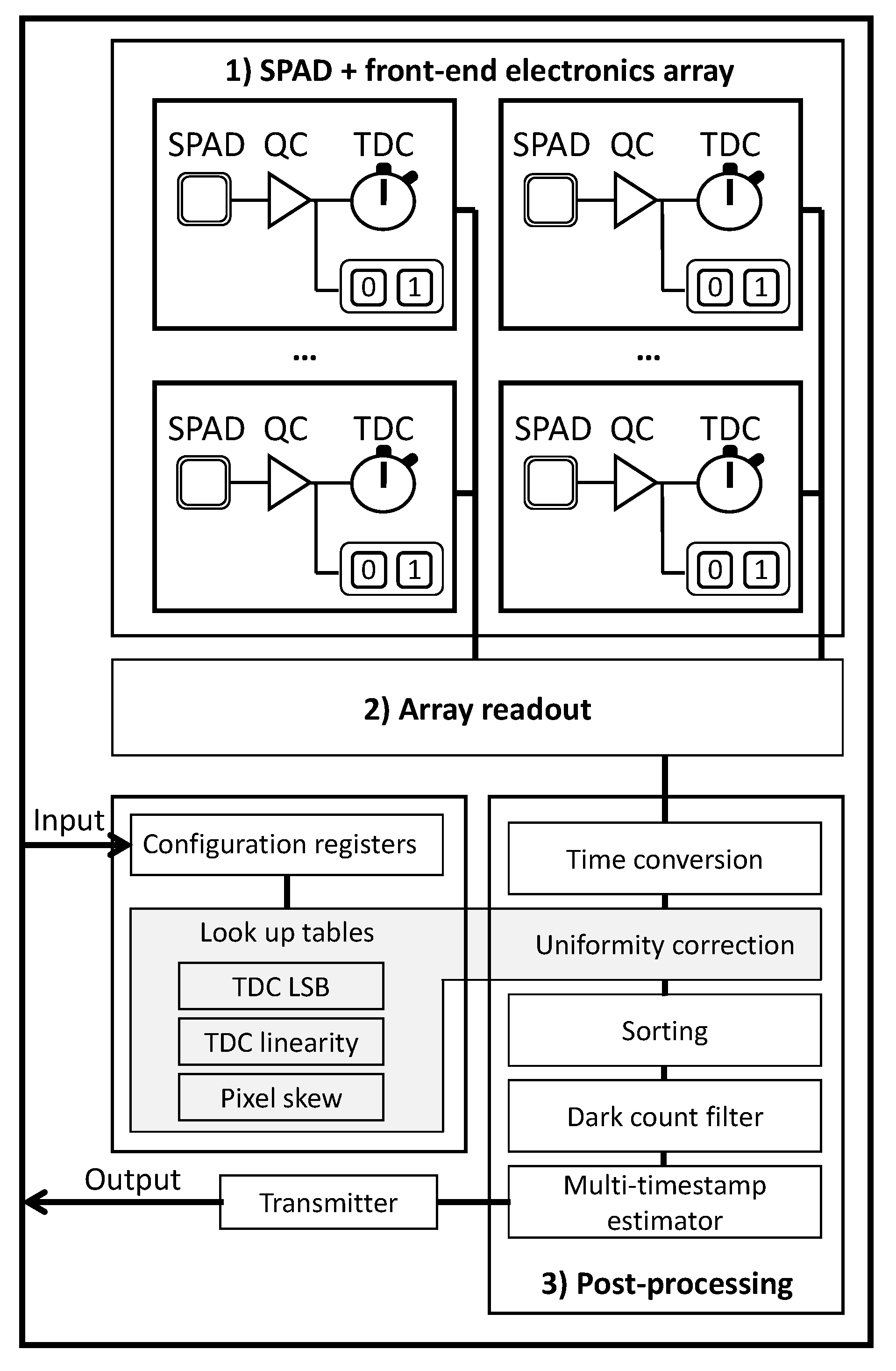
- Nolet, F.; Lemaire, W.; Dubois, F.; Roy, N.; Carrier, S.G.; Samson, A.; Charlebois, S.A.; Fontaine, R.; Pratte, J.F. A 256 pixelated SPAD readout ASIC with in-Pixel TDC and embedded digital processing for uniformity and skew correction. Nucl. Instrum. Methods Phys. Res. Sect. A Accel. Spectrom. Detect. Assoc. Equip. 2020, 949. [Google Scholar] [CrossRef]
- Bigas, M.; Cabruja, E.; Forest, J.; Salvi, J. Review of CMOS image sensors. Microelectron. J. 2006, 37, 433–451. [Google Scholar] [CrossRef] [Green Version]
- El-Desouki, M.; Jamal Deen, M.; Fang, Q.; Liu, L.; Tse, F.; Armstrong, D. CMOS image sensors for high speed applications. Sensors 2009, 9, 430–444. [Google Scholar] [CrossRef] [PubMed]
- Radeka, V. Low noise techniques in detectors. Ann. Rev. Nucl. Part. Sci. 1988, 38, 217–277. [Google Scholar] [CrossRef]
- Garutti, E.; Musienko, Y. Radiation damage of SiPMs. Nucl. Instrum. Methods Phys. Res. Sect. A Accel. Spectrom. Detect. Assoc. Equip. 2019, 926, 69–84. [Google Scholar] [CrossRef] [Green Version]
- Frach, T.; Prescher, G. Digital Silicon Photomultiplier for TOF PET. U.S. Patent US8395127, 19 March 2013. [Google Scholar]
- Cova, S.; Ghioni, M.; Lacaita, A.; Samori, C.; Zappa, F. Avalanche photodiodes and quenching circuits for single-photon detection. Appl. Opt. 1996, 35, 1956–1976. [Google Scholar] [CrossRef] [PubMed]
- Vachon, F.; Parent, S.; Nolet, F.; Dautet, H.; Pratte, J.F.; Charlebois, S.A. Measuring count rates free from correlated noise in digital silicon photomultipliers. Meas. Sci. Technol. 2020. [Google Scholar] [CrossRef]
- Lo, S.H.; Buchanan, D.A.; Taur, Y.; Wang, W. Quantum-mechanical modeling of electron tunneling current from the inversion layer of ultra-thin-oxide nMOSFET’s. IEEE Electron Device Lett. 1997, 18, 209–211. [Google Scholar] [CrossRef]
- Frach, T.; Prescher, G.; Degenhardt, C.; de Gruyter, R.; Schmitz, A.; Ballizany, R. The digital Silicon Photomultiplier—Principle of operation and intrinsic detector performance. In Proceedings of the 2009 IEEE Nuclear Science Symposium and Medical Imaging Conference, Orlando, FL, USA, 25–31 October 2009; pp. 1959–1965. [Google Scholar]
- Perenzoni, M.; Pancheri, L.; Stoppa, D. Compact SPAD-Based pixel architectures for time-resolved image sensors. Sensors 2016, 16, 745. [Google Scholar] [CrossRef]
- Bérubé, B.L.; Rhéaume, V.P.; Therrien, A.C.; Parent, S.; Maurais, L.; Boisvert, A.; Carini, G.; Charlebois, S.A.; Fontaine, R.; Pratte, J.F. Development of a single photon avalanche diode (SPAD) array in high voltage CMOS 0.8 μm dedicated to a 3D integrated circuit (3DIC). In Proceedings of the Nuclear Science Symposium and Medical Imaging Conference (NSS/MIC), 2012 IEEE, Anaheim, CA, USA, 29 October–3 November 2012; pp. 1835–1839. [Google Scholar]
- Berube, B.L.; Rheaume, V.P.; Parent, S.; Maurais, L.; Therrien, A.; Charette, P.; Charlebois, S.; Fontaine, R.; Pratte, J.F. Implementation study of single photon avalanche diodes (SPAD) in 0.8 μm HV CMOS technology. IEEE Trans. Nucl. Sci. 2015, 62, 710–718. [Google Scholar] [CrossRef]
- Palubiak, D.P.; Deen, M.J. CMOS SPADs: Design issues and research challenges for detectors, circuits, and arrays. Spectroscopy 2014, 8, 10. [Google Scholar] [CrossRef]
- Gersbach, M.; Richardson, J.; Mazaleyrat, E.; Hardillier, S.; Niclass, C.; Henderson, R.; Grant, L.; Charbon, E. A low-noise single-photon detector implemented in a 130 nm CMOS imaging process. Solid State Electron. 2009, 53, 803–808. [Google Scholar] [CrossRef]
- Villa, F.; Bronzi, D.; Zou, Y.; Scarcella, C.; Boso, G.; Tisa, S.; Tosi, A.; Zappa, F.; Durini, D.; Weyers, S.; et al. CMOS SPADs with up to 500 μm diameter and 55% detection efficiency at 420 nm. J. Mod. Opt. 2014, 61, 102–115. [Google Scholar] [CrossRef]
- Gersbach, M.; Maruyama, Y.; Trimananda, R.; Fishburn, M.W.; Stoppa, D.; Richardson, J.A.; Walker, R.; Henderson, R.; Charbon, E. A time-resolved, low-noise single-photon image sensor fabricated in deep-submicron CMOS technology. IEEE J. Solid State Circuits 2012, 47, 1394–1407. [Google Scholar] [CrossRef]
- Palubiak, D.; El-Desouki, M.M.; Marinov, O.; Deen, M.J.; Fang, Q. High-speed, single-photon avalanche-photodiode imager for biomedical applications. IEEE Sens. J. 2011, 11, 2401–2412. [Google Scholar] [CrossRef]
- nEXO Collaboration; Kharusi, S.A.; Alamre, A.; Albert, J.B.; Alfaris, M.; Anton, G.; Arnquist, I.J.; Badhrees, I.; Barbeau, P.S.; Beck, D.; et al. nEXO pre-conceptual design report. arXiv 2018, arXiv:1805.11142. [Google Scholar]
- Tisa, S.; Guerrieri, F.; Zappa, F. Variable-Load Quenching Circuit for single-photon avalanche diodes. Opt. Express 2008, 16, 2232–2244. [Google Scholar] [CrossRef]
- Chan, S.; Halimi, A.; Zhu, F.; Gyongy, I.; Henderson, R.K.; Bowman, R.; Mclaughlin, S.; Buller, G.S.; Leach, J. Long-range depth imaging using a single-photon detector array and non-local data fusion. Sci. Rep. 2019, 9. [Google Scholar] [CrossRef] [Green Version]
- Lemaire, W.; Nolet, F.; Dubois, F.; Therrien, A.C.; Pratte, J.F.; Fontaine, R. Embedded time of arrival estimation for digital silicon photomultipliers with in-pixel TDCs. Nucl. Instrum. Methods Phys. Res. Sect. A Accel. Spectrom. Detect. Assoc. Equip. 2020. [Google Scholar] [CrossRef]
- Pavia, J.M.; Scandini, M.; Lindner, S.; Wolf, M.; Charbon, E. A 1 x 400 backside-illuminated SPAD sensor with 49.7 ps resolution, 30 pJ/Sample TDCs fabricated in 3D CMOS technology for near-infrared optical tomography. J. Solid State Circuits 2015, 50, 2406–2418. [Google Scholar] [CrossRef]
- Aull, B.; Burns, J.; Chen, C.; Felton, B.; Hanson, H.; Keast, C.; Knecht, J.; Loomis, A.; Renzi, M.; Soares, A.; et al. Laser radar imager based on 3D integration of Geiger-mode avalanche photodiodes with two SOI timing circuit layers. In Digest of Technical Papers, Proceedings of the Solid-State Circuits Conference, San Francisco, CA, USA, 6–9 February 2006; IEEE International: Piscataway, NJ, USA, 2006; pp. 1179–1188. [Google Scholar]
- Baba, T.; Nagano, T.; Ishida, A.; Adachi, S.; Nakamura, S.; Yamamoto, K. Silicon hybrid SPAD with high-NIR-sensitivity for TOF applications (Paper 10108-33). In Proceedings of the SPIE Photonics West 2017, San Francisco, CA, USA, 28 January–2 February 2017. [Google Scholar]
- Moore, G.E. Cramming more components onto integrated circuits. Proc. IEEE 1998, 86, 82–85. [Google Scholar] [CrossRef]
- Radojcic, R. More-Than-Moore 2.5D and 3D SiP Integration, 1st ed.; Springer International Publishing: Cham, Switzerland, 2017. [Google Scholar]
- Kim, C.; Kim, D.; Jeong, W.; Kim, H.; Park, I.H.; Park, H.; Lee, J.; Park, J.; Ahn, Y.; Lee, J.Y.; et al. A 512-Gb 3-b/Cell 64-Stacked WL 3-D-NAND Flash Memory. IEEE J. Solid State Circuits 2018, 53, 124–133. [Google Scholar] [CrossRef]
- SONY. Sony Develops Next-Generation Back-Illuminated CMOS Image Sensor which Embodies the Continuous Evolution of the Camera; SONY: Tokyo, Japan, 2012. [Google Scholar]
- Tezzaron Semiconductor Corporation. Our Technology 101; Tezzaron Semiconductor Corporation: Austin, TX, USA, 2020. [Google Scholar]
- Deptuch, G.W.; Carini, G.; Grybos, P.; Kmon, P.; Maj, P.; Trimpl, M.; Siddons, D.P.; Szczygiel, R.; Yarema, R. Design and tests of the vertically integrated photon imaging chip. IEEE Trans. Nucl. Sci. 2014, 61, 663–674. [Google Scholar] [CrossRef]
- Tétrault, M.A.; Therrien, A.C.; Lamy, É.D.; Boisvert, A.; Fontaine, R.; Pratte, J.F. Dark count impact for first photon discriminators for SPAD digital arrays in PET. IEEE Trans. Nucl. Sci. 2015, 62, 719–726. [Google Scholar] [CrossRef]
- Aull, B.F.; Duerr, E.K.; Frechette, J.P.; McIntosh, K.A.; Schuette, D.R.; Younger, R.D. Large-format geiger-mode avalanche photodiode arrays and readout circuits. IEEE J. Sel. Top. Quantum Electron. 2018, 24, 1–10. [Google Scholar] [CrossRef]
- Aull, B.F.; Schuette, D.R.; Young, D.J.; Craig, D.M.; Felton, B.J.; Warner, K. A study of crosstalk in a 256 × 256 photon counting imager based on silicon geiger-mode avalanche photodiodes. IEEE Sens. J. 2015, 15, 2123–2132. [Google Scholar] [CrossRef]
- Nagano, T.; Tsuchiya, R.; Ishida, A.; Yamamoto, K. Development of new MPPC with higher NIR sensitivity and wider dynamic range (Paper 10108-21). In Proceedings of the SPIE Photonics West 2017, San Francisco, CA, USA, 28 January–2 February 2017. [Google Scholar]
- Mizuno, T.; Ikeda, H.; Makino, K.; Tamura, Y.; Suzuki, Y.; Baba, T.; Adachi, S.; Hashi, T.; Mita, M.; Mimasu, Y.; et al. Geiger-mode three-dimensional image sensor for eye-safe flash LIDAR. IEICE Electron. Express 2020. [Google Scholar] [CrossRef]
- Mizuno, T.; Ikeda, H.; Nagano, T.; Baba, T.; Mita, M.; Misamu, Y.; Hoshino, T. Three-dimensional image sensor with MPPC for flash LIDAR. Trans. Jpn. Soc. Aeronaut. Space Sci. 2020, 63, 42–49. [Google Scholar] [CrossRef] [Green Version]
- Diehl, I.; Hansen, K.; Krüger, K.; Reckleben, C.; Sefkow, F.; Andricek, L.; Jendrysik, C.; Ninkovic, J.; Petrovics, S.; Richter, R.; et al. Readout ASIC for fast digital imaging using SiPM sensors: Concept study. In Proceedings of the IEEE Nuclear Science Symposium and Medical Imaging Conference (NSS/MIC), San Diego, CA, USA, 31 October–7 November 2015; pp. 1–3. [Google Scholar] [CrossRef]
- DESY. Digital SiPM Pixel Detector; DESY: Hamburg, Germany, 2018. [Google Scholar]
- Ninković, J.; Andriček, L.; Liemann, G.; Lutz, G.; Moser, H.G.; Richter, R.; Schopper, F. SiMPl-Novel high QE photosensor. Nucl. Instrum. Methods Phys. Res. Sect. A Accel. Spectrom. Detect. Assoc. Equip. 2009, 610, 142–144. [Google Scholar] [CrossRef]
- Diehl, I.; Hansen, K.; Krüger, K.; Reckleben, C.; Sefkow, F.; Yao, Y.; Andricek, L.; Ninkovic, J.; Petrovics, S.; Richter, R. Readout of digital SiPMs. In Proceedings of the 2018 IEEE Nuclear Science Symposium and Medical Imaging Conference (NSS/MIC), San Diego, CA, USA, 31 October–7 November 2018; Volume 1, pp. 1–3. [Google Scholar]
- Pancheri, L.; Ficorella, A.; Brogi, P.; Collazuol, G.; Dalla Betta, G.; Marrocchesi, P.S.; Morsani, F.; Ratti, L.; Savoy-Navarro, A.; Sulaj, A. First demonstration of a two-tier pixelated avalanche sensor for charged particle detection. IEEE J. Electron Devices Soc. 2017, 5, 404–410. [Google Scholar] [CrossRef]
- Pancheri, L.; Brogi, P.; Collazuol, G.; Dalla Betta, G.F.; Ficorella, A.; Marrocchesi, P.; Morsani, F.; Ratti, L.; Savoy-Navarro, A. First prototypes of two-tier avalanche pixel sensors for particle detection. Nucl. Instrum. Methods Phys. Res. Sect. A Accel. Spectrom. Detect. Assoc. Equip. 2017, 845, 143–146. [Google Scholar] [CrossRef]
- Lindner, S.; Pellegrini, S.; Henrion, Y.; Rae, B.; Wolf, M.; Charbon, E. A high-pde, backside-illuminated SPAD in 65/40-nm 3D IC CMOS pixel with cascoded passive quenching and active recharge. IEEE Electron Device Lett. 2017, 38, 1547–1550. [Google Scholar] [CrossRef]
- Lee, M.; Ximenes, A.R.; Padmanabhan, P.; Wang, T.; Huang, K.; Yamashita, Y.; Yaung, D.; Charbon, E. High-performance back-illuminated three-dimensional stacked single-photon avalanche diode implemented in 45-nm CMOS technology. IEEE J. Sel. Top. Quantum Electron. 2018, 24, 1–9. [Google Scholar] [CrossRef]
- Ronchini Ximenes, A.; Padmanabhan, P.; Lee, M.; Yamashita, Y.; Yaung, D.; Charbon, E. A modular, direct time-of-flight depth sensor in 45/65-nm 3-D-Stacked CMOS technology. IEEE J. Solid State Circuits 2019, 54, 3203–3214. [Google Scholar] [CrossRef]
- Al Abbas, T.; Dutton, N.A.W.; Almer, O.; Pellegrini, S.; Henrion, Y.; Henderson, R.K. Backside illuminated SPAD image sensor with 7.83 μm pitch in 3D-stacked CMOS technology. In Proceedings of the 2016 IEEE International Electron Devices Meeting (IEDM), San Francisco, CA, USA, 3–7 December 2016; pp. 8.1.1–8.1.4. [Google Scholar] [CrossRef] [Green Version]
- Hutchings, S.W.; Johnston, N.; Gyongy, I.; Al Abbas, T.; Dutton, N.A.W.; Tyler, M.; Chan, S.; Leach, J.; Henderson, R.K. A reconfigurable 3-D-Stacked SPAD imager with in-pixel histogramming for flash LIDAR or high-speed time-of-flight imaging. IEEE J. Solid State Circuits 2019, 54, 2947–2956. [Google Scholar] [CrossRef] [Green Version]
- Albert, J.B.; Anton, G.; Arnquist, I.J.; Badhrees, I.; Barbeau, P.; Beck, D.; Belov, V.; Bourque, F.; Brodsky, J.P.; Brown, E.; et al. Sensitivity and discovery potential of the proposed nEXO experiment to neutrinoless double-β decay. Phys. Rev. C 2018, 97, 065503. [Google Scholar] [CrossRef] [Green Version]
- Bérubé, B.L. Conception de Matrices de Diodes Avalanche a Photon Unique sur Circuits Intégrés CMOS 3D; Universite de Sherbrooke: Sherbrooke, QC, Canada, 2014. [Google Scholar]
- Maurais, L. Conception d’un Procédé de Microfabrication Pour L’assemblage 3D Puce-à-Puce de Circuits Intégrés Hétérogènes à des Fins de Prototypage; Université de Sherbrooke: Sherbrooke, QC, Canada, 2018. [Google Scholar]
- Bernard, X. Développement d’un Procédé D’assemblage 3D Puce à Gaufre de Photocapteurs Hétérogènes; Université de Sherbrooke: Sherbrooke, QC, Canada, 2019. [Google Scholar]
- Maurais, L.; Charlebois, S.A.; Parent, S.; Rhéaume, V.P.; Pratte, J.F. Impact of a 3D microfabrication process on the dark count rate of single photon avalanche diodes. In Proceedings of the 2014 Nuclear Science Symposium and Medical Imaging Conference, Seattle, WA, USA, 8–15 November 2014. [Google Scholar]
- Acerbi, F.; Gundacker, S. Understanding and simulating SiPMs. Nucl. Instrum. Methods Phys. Res. Sect. A Accel. Spectrom. Detect. Assoc. Equip. 2019, 926, 16–35. [Google Scholar] [CrossRef]
- Giudice, A.; Ghioni, M.; Biasi, R.; Zappa, F.; Cova, S.; Maccagnani, P.; Gulinatti, A. High-rate photon counting and picosecond timing with silicon-SPAD based compact detector modules. J. Mod. Opt. 2007, 54, 225–237. [Google Scholar] [CrossRef]
- Lacaita, A.; Ghioni, M.; Cova, S. Double epitaxy improves single-photon avalanche diode performance. Electron. Lett. 1989, 25, 841–843. [Google Scholar] [CrossRef]
- Pratte, J.F.; Bernard, X.; Rheaume, V.P.; Parent, S.; Nolet, F.; Maurais, L.; Berube, B.L.; Dubois, F.; Dequivre, T.; Corbeil Therrien, A.; et al. Sherbrooke’s first 3D digital SiPM: Measurements, recommendations and future work. In Proceedings of the 2016 Nuclear Science Symposium and Medical Imaging Conference, Strasbourg, France, 29 October–6 November 2016. [Google Scholar]
- Lhostis, S.; Farcy, A.; Deloffre, E.; Lorut, F.; Mermoz, S.; Henrion, Y.; Berthier, L.; Bailly, F.; Scevola, D.; Guyader, F.; et al. Reliable 300 mm wafer level hybrid bonding for 3D stacked CMOS image sensors. In Proceedings of the IEEE 66th Electronic Components and Technology Conference (ECTC), Las Vegas, NV, USA, 31 May–3 June 2016; pp. 869–876. [Google Scholar] [CrossRef]
- Tassin, C.; Thenoz, Y.; Chabbal, J. Thinned backside illuminated CCDs for ultraviolet imaging. In Ultraviolet Technology II; Huffman, R.E., Ed.; International Society for Optics and Photonics, SPIE: Orlando, FL, USA, 1988; Volume 0932, pp. 305–310. [Google Scholar] [CrossRef]
- Hoenk, M.E.; Grunthaner, P.J.; Grunthaner, F.J.; Terhune, R.W.; Fattahi, M.M. Epitaxial growth of p+ silicon on a backside-thinned CCD for enhanced UV response. In High-Resolution Sensors and Hybrid Systems; International Society for Optics and Photonics, SPIE: San Jose, CA, USA, 1992; Volume 1656, pp. 488–496. [Google Scholar] [CrossRef]
- Fong, B.S.; Davies, M.; Deschamps, P. Timing resolution and time walk in SLiK SPAD: Measurement and optimization. In Optical Sensing, Imaging, and Photon Counting: Nanostructured Devices and Applications 2017; International Society for Optics and Photonics, SPIE: San Diego, CA, USA, 2017; Volume 10353, pp. 1–18. [Google Scholar] [CrossRef]
- Gulinatti, A.; Rech, I.; Panzeri, F.; Cammi, C.; Maccagnani, P.; Ghioni, M.; Cova, S. New silicon SPAD technology for enhanced red-sensitivity, high-resolution timing and system integration. J. Mod. Opt. 2012, 59, 1489–1499. [Google Scholar] [CrossRef]
- Lee, M.; Sun, P.; Pandraud, G.; Bruschini, C.; Charbon, E. First near-ultraviolet- and blue-enhanced backside-illuminated single-photon avalanche diode based on standard SOI CMOS technology. IEEE J. Sel. Top. Quantum Electron. 2019, 25, 1–6. [Google Scholar] [CrossRef]
- Palik, E.D. Handbook of Optical Constants of Solids; Academic Press: Cambridge, MA, USA, 1998; Volume 3. [Google Scholar]
- Janesick, J.; Elliott, T.; Frasehetti, G.; Collins, S.; Blouke, M.; Corrie, B. Charge-coupled device pinning technologies. In Optical Sensors and Electronic Photography; Blouke, M.M., Pophal, D., Eds.; International Society for Optics and Photonics, SPIE: Los Angeles, CA, USA, 1989; Volume 1071, pp. 153–169. [Google Scholar] [CrossRef]
- Heymes, J.; Soman, M.; Randall, G.; Gottwald, A.; Harris, A.; Kelt, A.; Moody, I.; Meng, X.; Holland, A.D. Comparison of back-thinned detector ultraviolet quantum efficiency for two commercially available passivation treatments. IEEE Trans. Nucl. Sci. 2020, 67, 1962–1967. [Google Scholar] [CrossRef]
- Hoenk, M.E.; Grunthaner, P.J.; Grunthaner, F.J.; Terhune, R.W.; Fattahi, M.; Tseng, H.F. Growth of a delta-doped silicon layer by molecular beam epitaxy on a charge-coupled device for reflection-limited ultraviolet quantum efficiency. Appl. Phys. Lett. 1992, 61, 1084–1086. [Google Scholar] [CrossRef]
- Hoenk, M.E.; Jones, T.J.; Dickie, M.R.; Greer, F.; Cunningham, T.J.; Blazejewski, E.R.; Nikzad, S. Delta-doped back-illuminated CMOS imaging arrays: Progress and prospects. In Infrared Systems and Photoelectronic Technology IV; Dereniak, E.L., Hartke, J.P., LeVan, P.D., Longshore, R.E., Sood, A.K., Eds.; International Society for Optics and Photonics, SPIE: San Diego, CA, USA, 2009; Volume 7419, pp. 187–201. [Google Scholar] [CrossRef]
- Hoenk, M.E.; Nikzad, S.; Carver, A.G.; Jones, T.J.; Hennessy, J.; Jewell, A.D.; Sgro, J.; Tsur, S.; McClish, M.; Farrell, R. Superlattice-doped silicon detectors: Progress and prospects. In High Energy, Optical, and Infrared Detectors for Astronomy VI; Holland, A.D., Beletic, J., Eds.; International Society for Optics and Photonics, SPIE: Montréal, QC, Canada, 2014; Volume 9154, pp. 324–336. [Google Scholar] [CrossRef]
- Schuette, D.R.; Westhoff, R.C.; Ciampi, J.S.; Perlin, G.E.; Young, D.J.; Aull, B.F.; Reich, R.K.; Shaver, D.C. MBE back-illuminated silicon Geiger-mode avalanche photodiodes for enhanced ultraviolet response. In Advanced Photon Counting Techniques V; SPIE: Bellingham, WA, USA, 2011; Volume 8033, p. 80330D. [Google Scholar]
- Gola, A.; Acerbi, F.; Capasso, M.; Marcante, M.; Mazzi, A.; Paternoster, G.; Piemonte, C.; Regazzoni, V.; Zorzi, N. NUV-Sensitive silicon photomultiplier technologies developed at fondazione bruno kessler. Sensors 2019, 19, 308. [Google Scholar] [CrossRef] [PubMed] [Green Version]
- D’Ascenzo, N.; Antonecchia, E.; Brensing, A.; Brockherde, W.; Dreiner, S.; Ewering, J.; Kuhn, M.; Schmidt, A.; vom Stein, P.; Wang, W.; et al. A novel high photon detection efficiency silicon photomultiplier with shallow junction in 0.35 μm CMOS. IEEE Electron Device Lett. 2019, 40, 1471–1474. [Google Scholar] [CrossRef]
- Mazzillo, M.; Condorelli, G.; Sanfilippo, D.; Valvo, G.; Carbone, B.; Fallica, G.; Billotta, S.; Belluso, M.; Bonanno, G.; Cosentino, L.; et al. Silicon photomultiplier technology at STMicroelectronics. IEEE Trans. Nucl. Sci. 2009, 56, 2434–2442. [Google Scholar] [CrossRef]
- Hamden, E.T.; Greer, F.; Hoenk, M.E.; Blacksberg, J.; Dickie, M.R.; Nikzad, S.; Martin, D.C.; Schiminovich, D. Ultraviolet antireflection coatings for use in silicon detector design. Appl. Opt. 2011, 50, 4180–4188. [Google Scholar] [CrossRef] [Green Version]
- Lacaita, A.; Mastrapasqua, M.; Ghioni, M.; Vanoli, S. Observation of avalanche propagation by multiplication assisted diffusion in p-n junctions. Appl. Phys. Lett. 1990, 57, 489–491. [Google Scholar] [CrossRef] [Green Version]
- Excelitas Technologies Corp. Excelitas Single Photon Counting Modules SPCM-AQRH; Excelitas Technologies Corp: Waltham, MA, USA, 2020. [Google Scholar]
- Cova, S.; Lacaita, A.; Ghioni, M.; Ripamonti, G.; Louis, T.A. 20-ps timing resolution with single-photon avalanche diodes. Rev. Sci. Instrum. 1989, 60, 1104–1110. [Google Scholar] [CrossRef] [Green Version]
- Nolet, F.; Parent, S.; Roy, N.; Mercier, M.O.; Charlebois, S.; Fontaine, R.; Pratte, J.F. Quenching circuit and SPAD integrated in CMOS 65 nm with 7.8 ps FWHM single photon timing resolution. Instruments 2018, 2, 19. [Google Scholar] [CrossRef] [Green Version]
- Acerbi, F.; Paternoster, G.; Gola, A.; Zorzi, N.; Piemonte, C. Silicon photomultipliers and single-photon avalanche diodes with enhanced NIR detection efficiency at FBK. Nucl. Instrum. Methods Phys. Res. Sect. A Accel. Spectrom. Detect. Assoc. Equip. 2018, 912, 309–314. [Google Scholar] [CrossRef]
- Ninković, J.; Eckhart, R.; Hartmann, R.; Holl, P.; Koitsch, C.; Lutz, G.; Merck, C.; Mirzoyan, R.; Moser, H.G.; Otte, A.N.; et al. The avalanche drift diode—A back illumination drift silicon photomultiplier. Nucl. Instrum. Methods Phys. Res. Sect. A Accel. Spectrom. Detect. Assoc. Equip. 2007, 580, 1013–1015. [Google Scholar] [CrossRef]
- Rossignol, J.; Turtos, R.M.; Gundacker, S.; Gaudreault, D.; Auffray, E.; Lecoq, P.; Bérubé-Lauzière, Y.; Fontaine, R. Time-of-flight computed tomography—Proof of principle. Phys. Med. Biol. 2020, 65, 085013. [Google Scholar] [CrossRef] [PubMed]
- Lecoq, P.; Morel, C.; Prior, J.; Visvikis, D.; Gundacker, S.; Auffray, E.; Krizan, P.; Turtos, R.M.; Thers, D.; Charbon, E.; et al. Roadmap toward the 10 ps time-of-flight PET challenge. Phys. Med. Biol. 2020, 65, 21RM01. [Google Scholar] [CrossRef] [PubMed]
- Enquist, P.; Fountain, G.; Petteway, C.; Hollingsworth, A.; Grady, H. Low Cost of Ownership scalable copper Direct Bond Interconnect 3D IC technology for three dimensional integrated circuit applications. In Proceedings of the IEEE International Conference on 3D System Integration, San Francisco, CA, USA, 28–30 September 2009; pp. 1–6. [Google Scholar]
- Enquist, P. Metal/Silicon oxide hybrid bonding. In Handbook of Wafer Bonding; Ramm, P., Lu, J.J.Q., Taklo, M.M.V., Eds.; Wiley-VCH Verlag & Co. KGaA: Weinheim, Germany, 2012; Chapter 13; pp. 261–278. [Google Scholar] [CrossRef]
- Lecoq, P.; Korzhik, M.; Vasiliev, A. Can transient phenomena help improving time resolution in scintillators? IEEE Trans. Nucl. Sci. 2014, 61, 229–234. [Google Scholar] [CrossRef]
- Nolet, F.; Roy, N.; Carrier, S.; Bouchard, J.; Fontaine, R.; Charlebois, S.A.; Pratte, J.F. 22 μW, 5.1 ps LSB, 5.5 ps RMS jitter Vernier time-to-digital converter in CMOS 65 nm for single photon avalanche diode array. Electron. Lett. 2020, 56, 424–426. [Google Scholar] [CrossRef]
- Finkelstein, H.; Hsu, M.J.; Zlatanovic, S.; Esener, S. Performance trade-offs in single-photon avalanche diode miniaturization. Rev. Sci. Instrum. 2007, 78, 103103. [Google Scholar] [CrossRef]
- Enne, R.; Steindl, B.; Hofbauer, M.; Zimmermann, H. Fast cascoded quenching circuit for decreasing afterpulsing effects in 0.35 μm CMOS. IEEE Solid State Circuits Lett. 2018, 1, 62–65. [Google Scholar] [CrossRef]
- Dervić, A.; Steindl, B.; Hofbauer, M.; Zimmermann, H. High-voltage active quenching and resetting circuit for SPADs in 0.35 μm CMOS for raising the photon detection probability. Opt. Eng. 2019, 58, 1–4. [Google Scholar] [CrossRef]
- Gulinatti, A.; Maccagnani, P.; Rech, I.; Ghioni, M.; Cova, S. 35 ps time resolution at room temperature with large area single photon avalanche diodes. Electron. Lett. 2005, 41, 272–274. [Google Scholar] [CrossRef]
- Rech, I.; Labanca, I.; Armellini, G.; Gulinatti, A.; Ghioni, M.; Cova, S. Operation of silicon single photon avalanche diodes at cryogenic temperature. Rev. Sci. Instrum. 2007, 78, 063105. [Google Scholar] [CrossRef]
- Acerbi, F.; Ferri, A.; Gola, A.; Zorzi, N.; Piemonte, C. Analysis of single-photon time resolution of FBK silicon photomultipliers. Nucl. Instrum. Methods Phys. Res. Sect. A Accel. Spectrom. Detect. Assoc. Equip. 2015, 787, 34–37. [Google Scholar] [CrossRef]
- Nolet, F. Électronique d’un Convertisseur Photon-Numérique 3D Pour une Résolution Temporelle de 10 ps FWHM. Ph.D. Thesis, Université de Sherbrooke, Sherbrooke, QC, Canada, 2020. [Google Scholar]
- Deschamps, J. Étude et Conception d’un Circuit Intégré Dédié à la Recherche et au Développement de Photodiodes Avalanches Monophotoniques; Université de Sherbrooke: Sherbrooke, QC, Canada, 2020. [Google Scholar]
- Braga, L.H.C.; Gasparini, L.; Grant, L.; Henderson, R.K.; Massari, N.; Perenzoni, M.; Stoppa, D.; Walker, R. A fully digital 8 × 16 SiPM array for PET applications with per-pixel TDCs and real-time energy output. IEEE J. Solid State Circuits 2014, 49, 301–314. [Google Scholar] [CrossRef]
- Villa, F.; Markovic, B.; Bellisai, S.; Bronzi, D.; Tosi, A.; Zappa, F.; Tisa, S.; Durini, D.; Weyers, S.; Paschen, U.; et al. SPAD smart pixel for time-of-flight and time-correlated single-photon counting measurements. IEEE Photonics J. 2012, 4, 795–804. [Google Scholar] [CrossRef]
- Tétrault, M.A.; Therrien, A.C.; Lemaire, W.; Fontaine, R.; Pratte, J.F. TDC array tradeoffs in current and upcoming digital SiPM detectors for time-of-flight PET. IEEE Trans. Nucl. Sci. 2017, 64, 925–932. [Google Scholar] [CrossRef]
- Roy, N.; Nolet, F.; Dubois, F.; Mercier, M.O.; Fontaine, R.; Pratte, J.F. Low power and small area, 6.9 ps RMS time-to-digital converter for 3-D digital SiPM. IEEE Trans. Radiat. Plasma Med. Sci. 2017, 1, 486–494. [Google Scholar] [CrossRef]
- Markovic, B.; Tisa, S.; Villa, F.A.; Tosi, A.; Zappa, F. A high-linearity, 17 ps precision time-to-digital converter based on a single-stage vernier delay loop fine interpolation. IEEE Trans. Circuits Syst. I Regul. Pap. 2013, 60, 557–569. [Google Scholar] [CrossRef]
- Lu, P.; Wu, Y.; Andreani, P. A 2.2-ps two-dimensional gated-vernier time-to-digital converter with digital calibration. IEEE Trans. Circuits Syst. II Express Briefs 2016, 63, 1019–1023. [Google Scholar] [CrossRef]
- Venialgo, E.; Mandai, S.; Gong, T.; Schaart, D.R.; Charbon, E. Time estimation with multichannel digital silicon photomultipliers. Phys. Med. Biol. 2015, 60, 2435–2452. [Google Scholar] [CrossRef]
- Corbeil Therrien, A.; Bérubé, B.L.; Charlebois, S.A.; Lecomte, R.; Fontaine, R.; Pratte, J.F. Modeling of single photon avalanche diode array detectors for PET applications. IEEE Trans. Nucl. Sci. 2014, 61, 14–22. [Google Scholar] [CrossRef]
- Therrien, A.; Lemaire, W.; Lecoq, P.; Fontaine, R.; Pratte, J.F. Energy discrimination for positron emission tomography using the time information of the first detected photons. J. Instrum. 2018, 13, P01012. [Google Scholar] [CrossRef]
- Jamil, A.; Ziegler, T.; Hufschmidt, P.; Li, G.; Lupin-Jimenez, L.; Michel, T.; Ostrovskiy, I.; Retière, F.; Schneider, J.; Wagenpfeil, M.; et al. VUV-Sensitive silicon photomultipliers for xenon scintillation light detection in nEXO. arXiv 2018, arXiv:1806.02220. [Google Scholar] [CrossRef] [Green Version]
- Amaudruz, P.A.; Baldwin, M.; Batygov, M.; Beltran, B.; Bina, C.; Bishop, D.; Bonatt, J.; Boorman, G.; Boulay, M.; Broerman, B.; et al. First results from the DEAP-3600 dark matter search with argon at SNOLAB. Phys. Rev. Lett. 2018, 121, 071801. [Google Scholar] [CrossRef] [PubMed] [Green Version]
- Wild, A. 3DIC Technology Using through Silicon vias Improves form Factor in Sensor Apps. 2016. Available online: www.sensorsmag.com (accessed on 16 January 2021).
- Hamamatsu. MPPCs (SiPMs)/MPPC Arrays; Hamamatsu: Hamamatsu City, Shizuoka, Japan, 2020. [Google Scholar]
- Broadcom. AFBR-S4N33C013: NUV-HD Single Silicon Photo Multiplier; Broadcom: San Jose, CA, USA, 2020. [Google Scholar]
- SensL. J-Series High PDE and Timing Resolution, TSV Package; SensL Division Office: Cork, Ireland, 2017. [Google Scholar]
- Fahim, F. Reconfigurable and Edgeless ROIC for Large Area Single-Photon Counting Imagers without Deadtime. Ph.D. Thesis, Northwestern University, Evanston, IL, USA, 2019. [Google Scholar]
- Fahim, F.; Deptuch, G.W.; Hoff, J.R.; Mohseni, H. Design methodology: Edgeless 3D ASICs with complex in-pixel processing for pixel detectors. In Optical Sensing, Imaging, and Photon Counting: Nanostructured Devices and Applications 2015; International Society for Optics and Photonics: Bellingham, WA, USA, 2015; Volume 9555, p. 95550M. [Google Scholar]
- Pustan, D.; Rastiagaev, E.; Wilde, J. In situ analysis of the stress development during fabrication processes of micro-assemblies. In Proceedings of the 59th Electronic Components and Technology Conference, San Diego, CA, USA, 26–29 May 2009; pp. 117–124. [Google Scholar] [CrossRef]
- Sunohara, M.; Sakaguchi, H.; Takano, A.; Arai, R.; Murayama, K.; Higashi, M. Studies on electrical performance and thermal stress of a silicon interposer with TSVs. In Proceedings of the 60th Electronic Components and Technology Conference (ECTC), Las Vegas, NV, USA, 1–4 June 2010; pp. 1088–1093. [Google Scholar] [CrossRef]
- IEEE Electronics Packaging Society. Chapter 8: Single chip and multi-chip integration. In Heterogeneous Integration Roadmap 2019 Edition, 2019th ed.; IEEE: Piscataway, NJ, USA, 2019. [Google Scholar]
- Sakai, T.; Sawyer, B.; Lu, H.; Takagi, Y.; Furuya, R.; Suzuki, Y.; Kobayashi, M.; Smet, V.; Sundaram, V.; Tummala, R. Design and demonstration of large 2.5D glass interposer for high bandwidth applications. In Proceedings of the IEEE CPMT Symposium Japan, Kyoto, Japan, 4–6 November 2014; pp. 138–141. [Google Scholar] [CrossRef]
- Sato, Y.; Kidera, N. Demonstration of 28 GHz Band Pass Filter Toward 5G Using Ultra Low Loss and High Accuracy Through Quartz Vias. In Proceedings of the IEEE 68th Electronic Components and Technology Conference (ECTC), San Diego, CA, USA, 29 May–1 June 2018; pp. 2243–2247. [Google Scholar] [CrossRef]
- von Trapp, F. Good News about Glass Substrates. In Francoise in 3D; 2019; Available online: www.3dincites.com (accessed on 16 January 2021).


Publisher’s Note: MDPI stays neutral with regard to jurisdictional claims in published maps and institutional affiliations. |
© 2021 by the authors. Licensee MDPI, Basel, Switzerland. This article is an open access article distributed under the terms and conditions of the Creative Commons Attribution (CC BY) license (http://creativecommons.org/licenses/by/4.0/).
Share and Cite
Pratte, J.-F.; Nolet, F.; Parent, S.; Vachon, F.; Roy, N.; Rossignol, T.; Deslandes, K.; Dautet, H.; Fontaine, R.; Charlebois, S.A. 3D Photon-To-Digital Converter for Radiation Instrumentation: Motivation and Future Works. Sensors 2021, 21, 598. https://doi.org/10.3390/s21020598
Pratte J-F, Nolet F, Parent S, Vachon F, Roy N, Rossignol T, Deslandes K, Dautet H, Fontaine R, Charlebois SA. 3D Photon-To-Digital Converter for Radiation Instrumentation: Motivation and Future Works. Sensors. 2021; 21(2):598. https://doi.org/10.3390/s21020598
Chicago/Turabian StylePratte, Jean-François, Frédéric Nolet, Samuel Parent, Frédéric Vachon, Nicolas Roy, Tommy Rossignol, Keven Deslandes, Henri Dautet, Réjean Fontaine, and Serge A. Charlebois. 2021. "3D Photon-To-Digital Converter for Radiation Instrumentation: Motivation and Future Works" Sensors 21, no. 2: 598. https://doi.org/10.3390/s21020598