Back-Gate GaN Nanowire-Based FET Device for Enhancing Gas Selectivity at Room Temperature


1
Department of Electrical and Computer Engineering, George Mason University, Fairfax, VA 22030, USA
2
N5 Sensors, Inc., Rockville, MD 20850, USA
*
Authors to whom correspondence should be addressed.
Sensors 2021, 21(2), 624; https://doi.org/10.3390/s21020624
Submission received: 16 December 2020
/
Revised: 5 January 2021
/
Accepted: 16 January 2021
/
Published: 17 January 2021
(This article belongs to the Special Issue Semiconductor Sensor)
Abstract
:In this work, a TiO2-coated GaN nanowire-based back-gate field-effect transistor (FET) device was designed and implemented to address the well-known cross-sensitive nature of metal oxides. Even though a two-terminal TiO2/GaN chemiresistor is highly sensitive to NO2, it suffers from lack of selectivity toward NO2 and SO2. Here, a Si back gate with C-AlGaN as the gate dielectric was demonstrated as a tunable parameter, which enhances discrimination of these cross-sensitive gases at room temperature (20 °C). Compared to no bias, a back-gate bias resulted in a significant 60% increase in NO2 response, whereas the increase was an insignificant 10% in SO2 response. The differential change in gas response was explained with the help of a band diagram, derived from the energetics of molecular models based on density functional theory (DFT). The device geometries in this work are not optimized and are intended only for proving the concept.
1. Introduction
For a gas sensor to be widely accepted for Internet of Things (IoT) applications, it must have high response, precise selectivity, quick response–recovery, low cost, small size, low power, long operating life, and stable operation across various environmental conditions. Unfortunately, no such gas sensor has yet been reported having all these desired properties. Metal oxide-based sensors have been employed to detect toxic environmental gases for several years [1]. They have the capability of providing all the above-mentioned gas sensing properties except precise selectivity. This is because their sensing mechanism generally involves the chemical interaction between the gas molecule and the oxygen chemisorbed on the sensing surface [2]. Gas molecules having similar chemical properties take part in this oxygen interaction, irrespective of the oxidizing or reducing nature of metal oxides [3]. Thus, cross-sensitivity among different analyte gases is inevitable in a metal oxide-based sensor device. For instance, the detection of NO2 and SO2 gas is hampered due to cross-interference when emitted in a mixed condition from a stationary source [4]. Systematic variations in the parameters such as dopants, additives, operating temperatures, bias voltage, grain size, and morphology have been adopted to achieve the necessary selectivity among various analytes [5]. Although efforts have been made, the problem of cross-sensitivity cannot yet be fully eliminated. This oxide-inherent cross-sensitive issue of a chemiresistive sensor can be resolved by employing several techniques, including a sensor array [6,7] and a field-effect transistor (FET) sensor [8].
Nanowires exhibit one-dimensional nanostructures that offer large surface-to-volume ratio, suitable for gas-sensing applications [9,10]. In the past few years, several nanowire-based gas sensors have been reported showing enhanced sensing performance in comparison to their bulk counterpart [11,12,13]. However, the analyte selectivity issue remains a challenge to be resolved, especially for metal-oxide sensors [14,15]. In this work, back-gate configuration was exploited in a GaN nanowire FET sensor for the differentiation of cross-sensitive gases. A Si back gate with C-AlGaN as the gate dielectric was formed on a TiO2/GaN nanowire to develop the back-gate FET device. Electrical and gas characterizations were conducted on the sensor devices in the presence of UV light at room temperature. Then, gas response enhancement and the sensing mechanism were described using an energy band diagram based on density functional theory (DFT) molecular models.
2. Experimental Details
Here, GaN nanowires were made from the Si-doped GaN epilayer using the top-down fabrication process. They were developed on a silicon substrate with a combination of industry standard stepper lithography and inductively coupled plasma (ICP) etching of a GaN/AlGaN epilayer grown on a Si substrate. The nanowire size was observed as being quite uniform. Having a length and a width of ~10 µm and ~400 nm, respectively. Subsequently, ohmic metal contacts composed of Ti (40 nm)/Al (80 nm)/Ti (40 nm)/Au (40 nm) were deposited upon the nanowire. Next, a passivation layer of SiO2 was formed on the nanowire device using the standard plasma-enhanced chemical vapor deposition (PECVD) technique. Later, a functionalization window on the GaN nanowire was developed by reactive-ion etching (RIE) of the SiO2 layer. A thin layer (5–10 nm) of TiO2 nanoclusters was deposited on the nanowire surface by RF magnetron sputtering followed by rapid thermal annealing (RTA). The fabrication details and process flow diagram of the nanowire-based two-terminal device can be found in our previous papers [16,17,18,19]. The C-doped AlGaN buffer layer (~200 nm) formed in between the GaN epilayer and the Si substrate was used as the gate dielectric here to develop a back-gate FET configuration (Figure 1). This dielectric layer was grown on top of the 300 µm thick Si substrate. To best of our knowledge, this is the first back-gate bias study using AlGaN as a gate dielectric in GaN-nanostructured devices. Finally, the fabricated FET device was placed and wire-bonded to a 24-pin ceramic dual in-line package (DIP).
All the current–voltage measurements of the FET device were performed using a National Instrument (NI) PXI SMU system (Rockville, MD, USA) under an LED UV light source having a wavelength of 365 nm and a power of 470 mW/cm2. The FET sensor was inserted in a mini gas chamber made of stainless steel for obtaining gas responses. Then, a mixture of NO2 or SO2 gas and breathing air was introduced into the chamber with a net flow (air + gas) of 0.5 slpm. The device current response was collected by the NI PXI SMU system and converted to a resistance value. Sensor response was evaluated as (Rg-Ra)/Ra, where Rg and Ra are resistances in the presence of the gas–air mixture and air, respectively.
3. Results and Discussion
The device properties of the fabricated GaN nanowires were discussed in detail in our previous work [20]. Here, the nanowire depletion region thickness and, consequently, its resistance was modulated by applying the back-gate bias voltage. Due to the thick dielectric layer and substrate used in this study, the fabricated FET requires a relatively high back-gate voltage, but it can be reduced by optimizing the thicknesses of the AlGaN layer and the Si substrate.
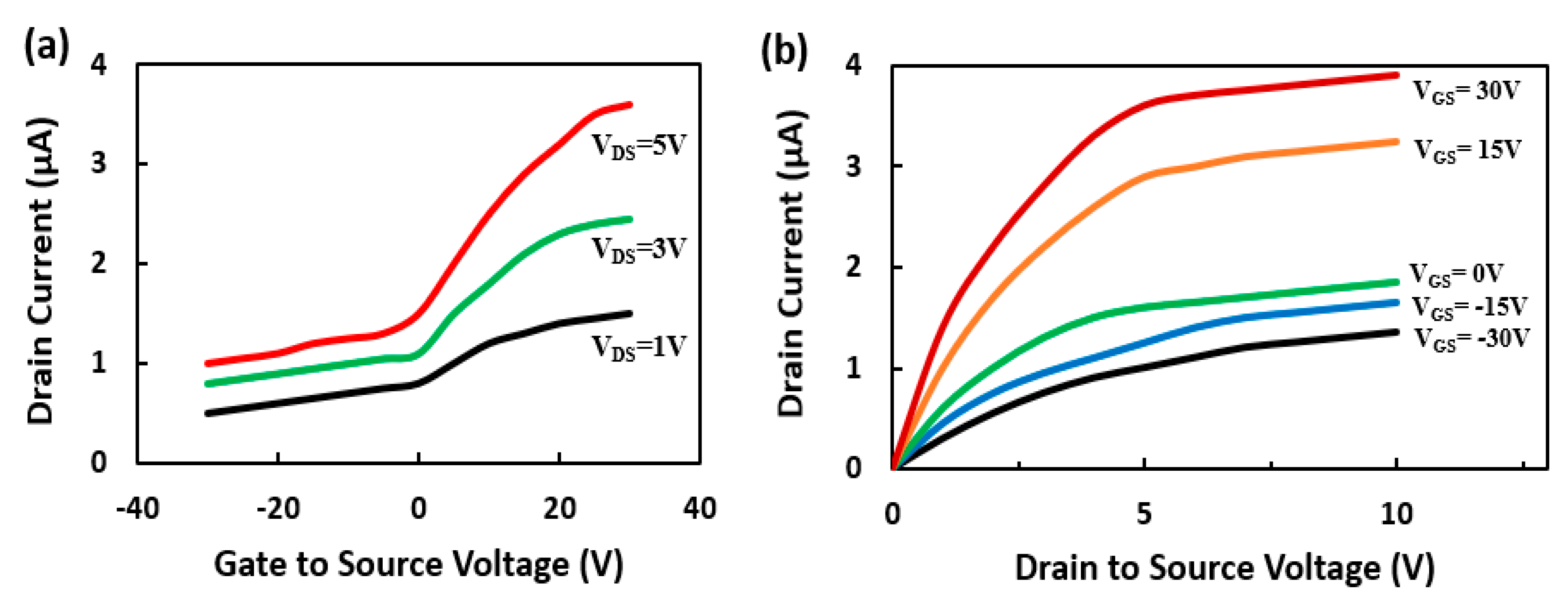
Since Si-doped GaN nanowire exhibits n-type behavior, the developed nanowire-based FET showed n-channel field-effect transistor characteristics operating in the depletion mode. When a bias voltage is applied to a Si back gate, the drain-to-source current is modulated within the GaN nanowire. Figure 2a demonstrates the drain current behavior with respect to VGS varied from −30 V to +30 V at a step of 5 V. The drain-to-source voltage (VDS) was kept constant at 1, 3, and 5 V. Figure 2b shows the plot of IDS vs. VDS for the GaN nanowire FET device with VDS varied from 0 V to 10 V. The drain currents presented here are for back-gate (VGS) voltages of −30 V, −15 V, 0 V, 15 V, and 30 V. The FET shows a typical drain current saturation with knee voltage at about 5 V. The electron field effect mobility (µ) was calculated using the following equation: [21,22]
where the transconductance, gm, is the slope of the IDS/VGS plot for a particular VDS, L and d are the length and width of the nanowire, respectively, tox is the gate dielectric thickness, and ε is the series permittivity of Si and AlGaN. Maximum gm derived from the plot was 0.07 µA/V at a VDS of 5 V, and the corresponding mobility was calculated as 112 cm2 V−1 s−1, which is close to the Hall measurement value of 105 cm2 V−1 s−1.
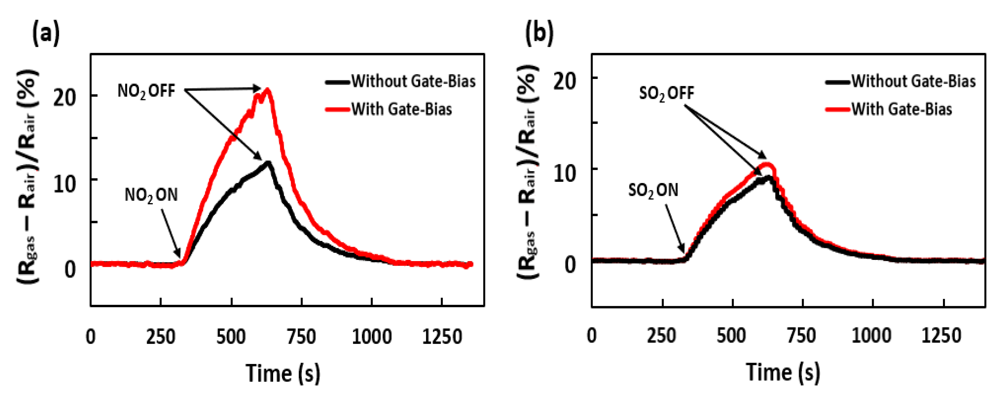
The gas sensing data were obtained in dry air under UV light at room temperature. The device was allowed to obtain a stable baseline signal by flowing dry air for 10 min before exposing it to the analyte gas for 250 s. When the gas flow was turned off, the sensor was kept for 10 min for baseline recovery without any purging. The normalized resistance responses of the TiO2/GaN nanowire-based sensor device when exposed to 10 ppm of NO2 and SO2 gas are shown in Figure 3. Without any gate bias, the sensor acts as a two-terminal resistor and exhibits a similar response magnitude for the two target gases. It is clearly seen that, upon applying a positive gate bias of 30 V, the NO2 response was enhanced by almost a 60% increase, whereas the SO2 response remains almost the same with only a marginal 10% increase. Thus, the selectivity of the FET sensor was improved for NO2 gas due to the lowering of cross-sensitive interference from SO2 gas. The change in sensor responses is mainly attributed to the modification of the channel depletion region with gate bias voltage. Consequently, the device’s Fermi energy level is shifted and the charge transfer between gas and sensor surface is altered. We fabricated a total of five FET devices of the same type and performed similar electrical and gas characterizations. It was observed that all of the back-gate FET sensors exhibited similar differential enhancement of responses toward the two analyte gases, indicating an insignificant device variability.
4. Gas-Sensing Mechanism
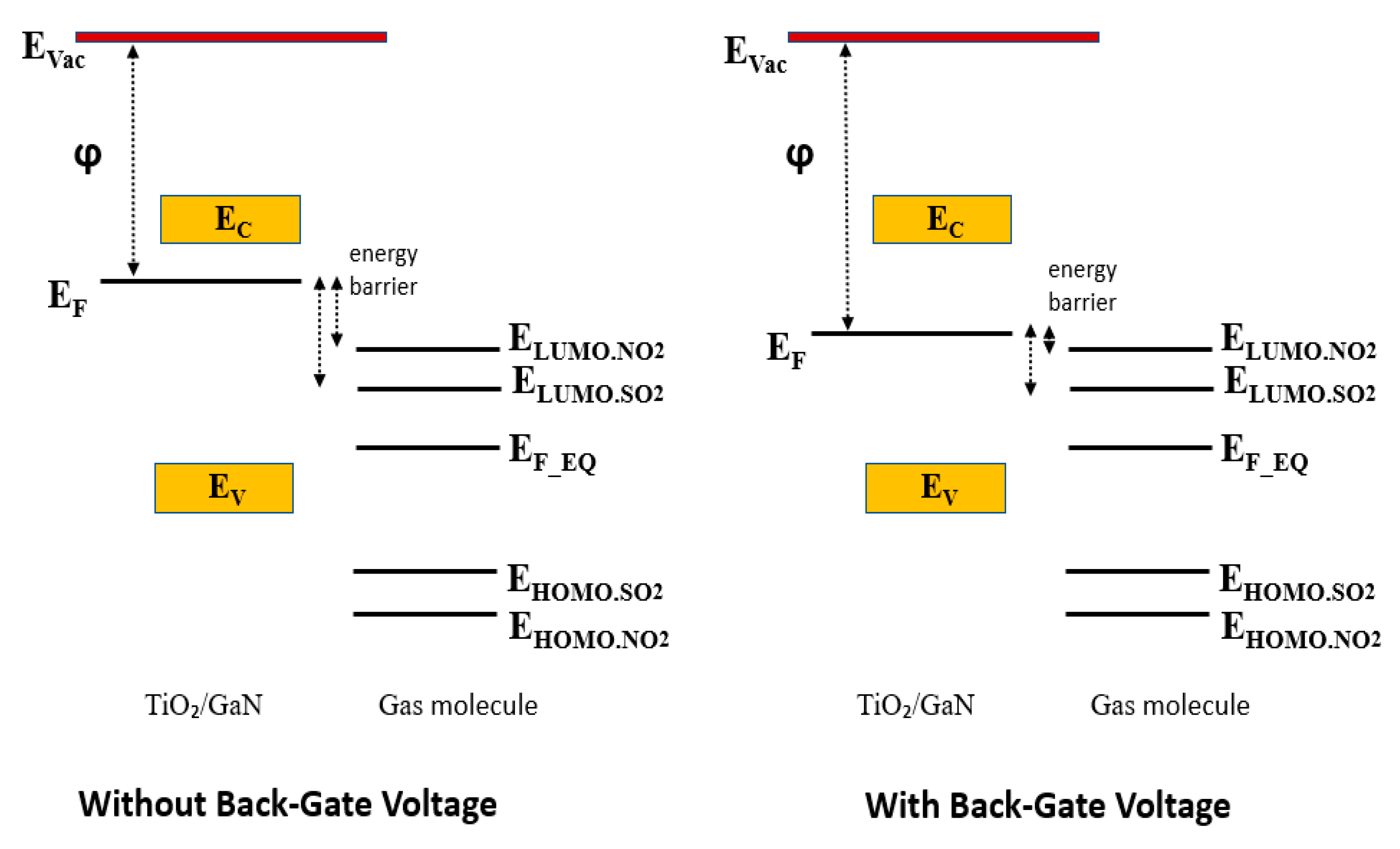
The gas-sensing mechanism of the TiO2/GaN nanowire-based device was explained with the help of an energy band diagram and a charge transfer process between the metal oxide and the gas molecule. The charge transfer process between the metal oxide surface and gas molecules controls the level of chemical interaction between them. It is well known that direction and value of charge transfer in the adsorption system depend on the work function of sensing material as well as the highest occupied molecular orbital (HOMO) and lowest unoccupied molecular orbital (LUMO) of the target gas. The charge transfer continues to take place until equilibrium Fermi energy is reached within the adsorption system.
A schematic of the energy band diagram showing the energy barrier between the TiO2/GaN system and the gas molecule is shown in Figure 4. The Fermi energy of the TiO2/GaN system and the HOMO and LUMO of NO2 and SO2 used here were obtained from our previous study on molecular models of adsorption systems using first-principle calculations within DFT [23,24].
Since the energy gap between the Fermi energy in TiO2/GaN and the LUMO is much less than that of the HOMO, electrons from the sensing surface prefer to move toward the LUMO of the gas molecule during adsorption. Here, the electrons are transferred from the metal oxide to the gas molecule by the process of quantum tunneling, which can be described by a single-step barrier concept [25]. It is well known that the probability of charge transmission through the energy step increases exponentially with the decrease in barrier height [26]. After applying the gate bias, the LUMO of NO2 was much closer to the TiO2/GaN Fermi level than the LUMO of SO2. That means that the probability of electron transfer between sensor and gas becomes comparatively higher in the case of NO2 adsorption. This increased charge transfer amount, on applying the gate bias, is reflected in the form of a significant gas response change as shown in Figure 3a. Therefore, the TiO2/GaN FET sensor becomes strongly selective toward NO2 against interfering gases such as SO2, with the gate bias being another tunable parameter. The Fermi energy of the two-terminal TiO2/GaN device without gate bias voltage, the HOMO and LUMO of NO2 and SO2 aligned to the vacuum level, as well as the absolute value of energy differences between the LUMO and Fermi energy (EF-LUMO) and energy differences between the HOMO and Fermi energy (EF-HOMO) are shown in Table 1.
5. Conclusions
In this work, we presented a GaN nanowire-based back-gate FET sensor device to address the cross-sensitivity among interfering gases NO2 and SO2. By applying a back-gate bias voltage to the Si substrate of a two-terminal TiO2/GaN sensor, selectivity toward NO2 was enhanced. It was found that the NO2 response was improved by 60% as compared to an insignificant 10% increase in the SO2 response, after applying the back-gate bias. The differential gas response due to the back-gate bias was discussed with the help of an energy band diagram and a charge transfer process derived from the DFT energy calculation of a molecular model.
Author Contributions
Conceptualization, formal analysis, investigation, methodology, writing—original draft, writing—review and editing, M.A.H.K.; device fabrication, review and editing, R.D.; supervision, M.V.R. and A.M. All authors have read and agreed to the published version of the manuscript.
Funding
This research was funded by the NSF grant # ECCS1840712 and internal funding from N5 Sensors, Inc.
Institutional Review Board Statement
Not applicable.
Informed Consent Statement
Not applicable.
Data Availability Statement
Not applicable.
Acknowledgments
This work was supported by the NSF grant # ECCS1840712 and internal funding from N5 Sensors, Inc., Rockville, MD, USA. The TiO2/GaN FET sensing devices were fabricated in the Nanofab of the NIST Center for Nanoscale Science and Technology, Gaithersburg, MD, USA. Gas sensing measurements were conducted at N5 Sensors, Inc.
Conflicts of Interest
The authors declare no conflict of interest.
References
- Khan, M.A.H.; Rao, M.V.; Li, Q. Recent Advances in Electrochemical Sensors for Detecting Toxic Gases: NO2, SO2 and H2S. Sensors 2019, 19, 905. [Google Scholar] [CrossRef] [PubMed] [Green Version]
- Ree, J.; Kim, A.Y.H.; Shin, H.K. Dynamics of Gas−Surface Interactions: Reaction of Atomic Oxygen with Chemisorbed Hydrogen on Tungsten. J. Phys. Chem. A 1997, 101, 4523–4534. [Google Scholar] [CrossRef]
- Dey, A. Semiconductor metal oxide gas sensors: A review. Mater. Sci. Eng. B 2018, 229, 206–217. [Google Scholar] [CrossRef]
- Johansson, J.K.E.; Mellqvist, J.; Samuelsson, J.; Offerle, B.; Lefer, B.; Rappenglück, B.; Flynn, J.; Yarwood, G. Emission measurements of alkenes, alkanes, SO2, and NO2 from stationary sources in Southeast Texas over a 5 year period using SOF and mobile DOAS. J. Geophys. Res. Atmos. 2014, 119, 1973–1991. [Google Scholar] [CrossRef] [Green Version]
- Sun, Y.-F.; Liu, S.-B.; Meng, F.; Liu, J.; Jin, Z.; Kong, L. Metal Oxide Nanostructures and Their Gas Sensing Properties: A Review. Sensors 2012, 12, 2610–2631. [Google Scholar] [CrossRef] [PubMed] [Green Version]
- Khan, M.A.H.; Thomson, B.; Debnath, R.; Motayed, A.; Rao, M.V. Nanowire-Based Sensor Array for Detection of Cross-Sensitive Gases Using PCA and Machine Learning Algorithms. IEEE Sens. J. 2020, 20, 6020–6028. [Google Scholar] [CrossRef]
- Khan, M.A.H.; Motayed, A.; Rao, M.V. Identification and quantification of gases and their mixtures using GaN sensor array and artificial neural network. Meas. Sci. Technol. 2020. [Google Scholar] [CrossRef]
- Rani, A.; DiCamillo, K.; Khan, M.A.H.; Paranjape, M.; E Zaghloul, M. Tuning the Polarity of MoTe2 FETs by Varying the Channel Thickness for Gas-Sensing Applications. Sensors 2019, 19, 2551. [Google Scholar] [CrossRef] [Green Version]
- Khan, M.A.H.; Rao, M.V. Gallium Nitride (GaN) Nanostructures and Their Gas Sensing Properties: A Review. Sensors 2020, 20, 3889. [Google Scholar] [CrossRef]
- Wang, Z.L. Novel Nanostructures and Nanodevices of ZnO. In Zinc Oxide Bulk, Thin Films and Nanostructures; Elsevier: Amsterdam, The Netherlands, 2006; pp. 339–370. [Google Scholar]
- Chen, X.; Wong, C.K.; Yuan, C.A.; Zhang, G. Nanowire-based gas sensors. Sens. Actuators B Chem. 2013, 177, 178–195. [Google Scholar] [CrossRef]
- Kumar, R.; Aldossary, O.M.; Kumar, G.; Umar, A. Zinc Oxide Nanostructures for NO2 Gas–Sensor Applications: A Review. Nano-Micro Lett. 2015, 7, 97–120. [Google Scholar] [CrossRef] [PubMed] [Green Version]
- Choi, Y.; Hwang, I.-S.; Park, J.-G.; Lee, J.-H. Novel fabrication of an SnO2nanowire gas sensor with high sensitivity. Nanotechnology 2008, 19, 095508. [Google Scholar] [CrossRef] [PubMed]
- Aluri, G.S.; Motayed, A.; Davydov, A.V.; Oleshko, V.P.; Bertness, K.; A Sanford, N.; Rao, M.V. Highly selective GaN-nanowire/TiO2-nanocluster hybrid sensors for detection of benzene and related environment pollutants. Nanotechnology 2011, 22, 295503. [Google Scholar] [CrossRef] [PubMed] [Green Version]
- Aluri, G.S.; Motayed, A.; Davydov, A.V.; Oleshko, V.P.; Bertness, K.; Rao, M.V. Nitro-Aromatic Explosive Sensing Using GaN Nanowire-Titania Nanocluster Hybrids. IEEE Sens. J. 2013, 13, 1883–1888. [Google Scholar] [CrossRef]
- Shi, C.; Rani, A.; Thomson, B.; Debnath, R.; Motayed, A.; Ioannou, D.E.; Li, Q. High-performance room-temperature TiO2-functionalized GaN nanowire gas sensors. Appl. Phys. Lett. 2019, 115, 121602. [Google Scholar] [CrossRef]
- Khan, M.A.H.; Thomson, B.; Debnath, R.; Rani, A.; Motayed, A.; Rao, M.V. Reliable anatase-titania nanoclusters functionalized GaN sensor devices for UV assisted NO2 gas-sensing in ppb level. Nanotechnology 2020, 31, 155504. [Google Scholar] [CrossRef]
- Khan, M.A.H.; Thomson, B.; Yu, J.; Debnath, R.; Motayed, A.; Rao, M.V. Scalable metal oxide functionalized GaN nanowire for precise SO2 detection. Sens. Actuators B Chem. 2020, 318, 128223. [Google Scholar] [CrossRef]
- Khan, M.A.H.; Debnath, R.; Motayed, A.; Rao, M.V. Accelerated Stress Tests and Statistical Reliability Analysis of Metal-Oxide/GaN Nanostructured Sensor Devices. IEEE Trans. Device Mater. Reliab. 2020, 20, 742–747. [Google Scholar] [CrossRef]
- Aluri, G.S.; Motayed, A.; Davydov, A.V.; Oleshko, V.P.; A Bertness, K.; A Sanford, N.; Mulpuri, R.V. Methanol, ethanol and hydrogen sensing using metal oxide and metal (TiO2–Pt) composite nanoclusters on GaN nanowires: A new route towards tailoring the selectivity of nanowire/nanocluster chemical sensors. Nanotechnology 2012, 23, 175501. [Google Scholar] [CrossRef] [Green Version]
- Huang, Y. Directed Assembly of One-Dimensional Nanostructures into Functional Networks. Science 2001, 291, 630–633. [Google Scholar] [CrossRef] [Green Version]
- Motayed, A.; He, M.; Davydov, A.V.; Melngailis, J.; Mohammad, S.N. Realization of reliable GaN nanowire transistors utilizing dielectrophoretic alignment technique. J. Appl. Phys. 2006, 100, 114310. [Google Scholar] [CrossRef] [Green Version]
- Khan, M.A.H.; Thomson, B.; Motayed, A.; Li, Q.; Rao, M.V. Functionalization of GaN Nanowire Sensors With Metal Oxides: An Experimental and DFT Investigation. IEEE Sens. J. 2020, 20, 7138–7147. [Google Scholar] [CrossRef]
- Khan, M.A.H.; Thomson, B.; Motayed, A.; Li, Q.; Rao, M.V. Metal-oxide/GaN based NO2 Gas detection at room temperature: An experimental and density functional theory investigation. In Micro- and Nanotechnology Sensors, Systems, and Applications XII; SPIE: Anaheim, CA, USA, 2020; p. 103. [Google Scholar] [CrossRef]
- Zhang, D.; Wu, J.; Li, P.; Cao, Y. Room-temperature SO2 gas-sensing properties based on a metal-doped MoS2 nanoflower: An experimental and density functional theory investigation. J. Mater. Chem. A 2017, 5, 20666–20677. [Google Scholar] [CrossRef]
- Dib, C.O.; Orellana, O. Quantum and classical limits in a potential step. Eur. J. Phys. 2017, 38, 045403. [Google Scholar] [CrossRef]
Figure 1.
Fabricated TiO2/GaN nanowire field-effect transistor (FET) sensor. FESEM image of the two terminals. The TiO2/GaN device is shown on the top side.
Figure 1.
Fabricated TiO2/GaN nanowire field-effect transistor (FET) sensor. FESEM image of the two terminals. The TiO2/GaN device is shown on the top side.

Figure 2.
(a) IDS vs. VGS plot for the GaN nanowire-based FET device for a VDS of 1, 3, and 5 V. (b) IDS vs. VDS plot for the GaN nanowire-based FET device with VGS varied from −30 V to 30 V at a step of 15 V. All the measurements were done under UV light at room temperature (20 °C).
Figure 2.
(a) IDS vs. VGS plot for the GaN nanowire-based FET device for a VDS of 1, 3, and 5 V. (b) IDS vs. VDS plot for the GaN nanowire-based FET device with VGS varied from −30 V to 30 V at a step of 15 V. All the measurements were done under UV light at room temperature (20 °C).

Figure 3.
Sensor response to 10 ppm of (a) NO2 and (b) SO2 with and without applying gate bias voltage of 30 V under UV light in dry air at room temperature (20 °C).
Figure 3.
Sensor response to 10 ppm of (a) NO2 and (b) SO2 with and without applying gate bias voltage of 30 V under UV light in dry air at room temperature (20 °C).

Figure 4.
Schematic representation of the energy band diagram showing energy barriers between the TiO2/GaN nanocomposite and the gas molecule. Here, ϕ, EC, EV, and EF represent work function, conduction band, valence band, and Fermi energy of TiO2/GaN, respectively, EVac denotes the energy of vacuum level, and EF_EQ represents the equilibrium state of the adsorption system. ELUMO and EHOMO indicate the orbital energies of the gas molecules. LUMO = lowest unoccupied molecular orbital; HOMO = highest occupied molecular orbital.


Table 1.
Fermi energy, molecular frontier orbital energies, and energy differences. EF-LUMO is the absolute value calculated by EF (device)-ELUMO (gas). EF-HOMO is the absolute value calculated by EF (device)-EHOMO (gas).
Table 1.
Fermi energy, molecular frontier orbital energies, and energy differences. EF-LUMO is the absolute value calculated by EF (device)-ELUMO (gas). EF-HOMO is the absolute value calculated by EF (device)-EHOMO (gas).
| Adsorption System | Fermi Energy (eV) | LUMO (eV) | HOMO (eV) | EF-LUMO (eV) | EF-HOMO (eV) |
|---|---|---|---|---|---|
| TiO2/GaN | −2.137 | - | - | - | - |
| NO2 | - | −2.890 | −8.612 | 0.753 | 6.475 |
| SO2 | - | −3.182 | −7.015 | 1.045 | 4.878 |
Publisher’s Note: MDPI stays neutral with regard to jurisdictional claims in published maps and institutional affiliations. |
© 2021 by the authors. Licensee MDPI, Basel, Switzerland. This article is an open access article distributed under the terms and conditions of the Creative Commons Attribution (CC BY) license (http://creativecommons.org/licenses/by/4.0/).
Share and Cite
MDPI and ACS Style
Khan, M.A.H.; Debnath, R.; Motayed, A.; Rao, M.V. Back-Gate GaN Nanowire-Based FET Device for Enhancing Gas Selectivity at Room Temperature. Sensors 2021, 21, 624. https://doi.org/10.3390/s21020624
AMA Style
Khan MAH, Debnath R, Motayed A, Rao MV. Back-Gate GaN Nanowire-Based FET Device for Enhancing Gas Selectivity at Room Temperature. Sensors. 2021; 21(2):624. https://doi.org/10.3390/s21020624
Chicago/Turabian StyleKhan, Md Ashfaque Hossain, Ratan Debnath, Abhishek Motayed, and Mulpuri V. Rao. 2021. "Back-Gate GaN Nanowire-Based FET Device for Enhancing Gas Selectivity at Room Temperature" Sensors 21, no. 2: 624. https://doi.org/10.3390/s21020624
Note that from the first issue of 2016, this journal uses article numbers instead of page numbers. See further details here.