What Can Electric Noise Spectroscopy Tell Us on the Physics of Perovskites?


1
Dipartimento di Fisica “E.R. Caianiello”, Università degli Studi di Salerno, I-84084 Fisciano, Salerno, Italy
2
CNR-SPIN Salerno, c/o Università degli Studi di Salerno, I-84084 Fisciano, Salerno, Italy
*
Authors to whom correspondence should be addressed.
Coatings 2021, 11(1), 96; https://doi.org/10.3390/coatings11010096
Submission received: 12 December 2020
/
Revised: 7 January 2021
/
Accepted: 14 January 2021
/
Published: 17 January 2021
(This article belongs to the Special Issue Advance in Perovskite Thin Films)
Abstract
:Electric noise spectroscopy is a non-destructive and a very sensitive method for studying the dynamic behaviors of the charge carriers and the kinetic processes in several condensed matter systems, with no limitation on operating temperatures. This technique has been extensively used to investigate several perovskite compounds, manganese oxides (La1−xSrxMnO3, La0.7Ba0.3MnO3, and Pr0.7Ca0.3MnO3), and a double perovskite (Sr2FeMoO6), whose properties have recently attracted great attention. In this work are reported the results from a detailed electrical transport and noise characterizations for each of the above cited materials, and they are interpreted in terms of specific physical models, evidencing peculiar properties, such as quantum interference effects and charge density waves.

1. Introduction
Recently, perovskite materials have attracted great attention due to their electrical, transport, and magnetic properties [1,2,3,4]. In particular, the so-called magnetoresistance (MR) effect and the interplay between spin [5], orbital [6], charge, and structural degrees of freedom [7], have been investigated in polycrystals, single crystals, and thin films. All these phenomena have been the subject of a great deal of research, in view of possible applications in spin electronics and magnetism. In this respect, magnetoresistive materials are already used today in a number of commercially available devices, such as magnetic sensors [8,9], magnetic recording heads [10], and magnetic memories [11,12]. The magnetoresistance effect, when observed in metals, is normally very small and offers scarce possibilities for technological applications. However, the fast advancement of technology and new materials research in recent years may make them more feasible. Instead, larger magnetoresistive effects have been found in ferromagnetic metals and their alloys. The phenomenon is called anisotropic magnetoresistance (AMR) because the change in resistance, when a field is applied parallel to the current direction, is different from when the field is perpendicular to the current direction [13,14]. Moreover, typical components in modern read heads operate thanks to the so-called giant magnetoresistive (GMR) effect, where the magnetoresistance values are more than one order of magnitude larger than those seen in AMR materials. GMR compounds are made with thin layers of magnetic material separated by non-magnetic ones and, depending on their thickness, the magnetic layers couple either ferromagnetically or antiferromagnetically [15,16,17]. Finally, the colossal magnetoresistance (CMR) effect is also observed in pervoskite structure manganites. The term colossal has been chosen because of the very large change in resistance, essentially from an insulating to a conducting state, occurring on application of a magnetic field. Since large fields of the order of a few tesla are required to cause this resistance variation, CMR materials are still not currently considered for practical application as magnetic sensors and, in particular, as the reading element in recording heads. However, a number of other applications are being explored, including bolometers [18,19,20], where a change in temperature causes a change in conductivity driven by a metal-insulator transition, and in spin-tunneling devices, that exploit their half-metallicity [21,22]. Despite the large amount of studies about the magnetic and transport properties of these materials, electric noise characterizations, that can provide new insights on individual perovskite systems, have not been systematically reported [23,24,25,26,27,28].
The spontaneous charge random fluctuations in electron devices are usually called noise, and both terms, fluctuations and noise, are used interchangeably. The physics of fluctuations is of great conceptual importance and is a part of physical kinetics which studies the variations of physical quantities, occurring spontaneously or induced by external fields [29,30]. The investigation of fluctuation phenomena, which may be called “fluctuation spectroscopy”, is a very informative method for the study of kinetic processes in matter. It is often also a method that is much more sensitive than the measurement of average quantities, as demonstrated in superconducting thin films [31,32,33,34] and devices [35,36,37,38], in low-dimensional conductors [39,40,41,42], in carbon nanotubes [43,44,45,46,47] and magnetic composites [48,49], and in conventional [50,51] and innovative solar cells [52,53,54,55]. The role of the noise spectrum analyzer is similar to the role of a microscope: It enables us to visualize the microscopic motion and transitions of particles. For all these reasons, electric noise measurements can give interesting information on the conduction mechanisms and the dynamic behaviors of the charge carriers in the many physical systems.
Triggered by these motivations, noise spectroscopy experiments have been performed on several perovskite compounds (in the form of thin and ultrathin films) and the results of the analysis are presented in this work. In particular, in Sr2FeMoO6 (SFMO) thin films, a fluctuation-induced tunneling model satisfactorily explains the measured temperature dependence of the electrical conductance and the current-voltage - curves behavior. This model can be also extended to describe the resistance fluctuations, confirming the dominant role of intergranular tunneling processes in the conduction phenomena of SFMO polycrystalline samples [56]. Current-resistance (CR) effects in La1−xSrxMnO3 (LSMO) ultrathin films are also reported. The resistance vs. temperature curves show a negative CR effect in the whole investigated temperature range, while the - characteristics evidence a non-Ohmic regime. The noise measurements are explained in terms of a two-level tunneling systems (TLTS) model, involving different physical scenarios. Among them, the one developed in the case of manganite bi-crystal junctions seems to capture many of the obtained experimental results and applies naturally to the LSMO samples grown on SrTiO3 (STO) substrates in the presence of miscut induced terraces [57]. Different conduction mechanisms are identified in La0.7Ba0.3MnO3 (LBMO) thin films deposited on STO and MgO substrates, respectively. While a standard noise behavior is observed with STO substrates, an anomalous behavior is found in the MgO case. Such anomalous temperature dependence of the measured noise, in the ferromagnetic metallic region, for LBMO-MgO samples is interpreted by considering an enhanced spin ordering with increasing bias currents. This experimental evidence is explained in terms of a spin torque like model assuming that the metallicity of the system is improved by the application of increasing current [58]. Finally, it is also possible to use the electric noise spectroscopy to identify, among different transport mechanisms, the dominating one. This is the case of charge density waves (CDW) conduction in Pr0.7Ca0.3MnO3 (PCMO) epitaxial thin films, and of weak-localization (WL) effects in ultrathin manganite samples. In both cases, the occurrence of unusual noise contributions has been observed, together with an overall increase of the noise level [59,60].
2. Perovskite Compounds: General Concepts and Applicative Indications
Perovskite magnetic materials have been studied for almost 50 years. These systems offer a degree of chemical flexibility which allows the relation between the oxides structure, and electronic and magnetic properties that can be controlled in various ways, such as: Doping [61,62,63], magnetic field [64,65,66], electric field [67,68], temperature [69,70,71], pressure, and photoexcitation [72,73,74,75]. Research on these compounds has revealed the relevant phenomenon of magnetoresistance [76,77,78,79], and has led to the formulation of important physical concepts such as double exchange [1] and the Jahn–Teller polaron [80].
In particular, the double exchange (DE) mechanism was proposed by Zener as a way for the charge to move by the generation of a spin polarized state [81]. This DE process has been historically explained in two different ways. Originally Zener, starting from the insulating antiferromagnetic LaMnO3 system, where electrons are localized on the atomic orbitals, showed how it should gradually become more ferromagnetic upon hole doping (introduction of Mn4+). He considered the problem of the exchange between Mn3+ and Mn4+ ions via an oxygen ion and introduced the concept of simultaneous transfer of an electron from the Mn3+ to the oxygen and from the oxygen to the neighboring Mn4+. Such a transfer was called double exchange. In the case of magnetic atoms, the configurations Mn3+–O2−–Mn4+ and Mn4+–O2−–Mn3+ are degenerate if the spins of the two d shells are parallel, and the lowest energy of the system at low temperature corresponds to parallel alignment of the spins of the two adjacent cations. If the manganese spins are not parallel or if the Mn–O–Mn bond is bent, the electron transfer becomes more difficult and the mobility decreases. It follows that there is a direct connection between conductivity and ferromagnetism. The second way to visualize DE processes was presented in detail by Anderson and Hasegawa [82]. It involves a second-order process in which the two states described above go from one to the other using an intermediate state Mn3+–O2−–Mn3+. In this context, the effective hopping probability (HP) for the electron to move from one Mn-site to the next is proportional to the square of the HP involving the p-oxygen and d-manganese orbitals. In addition, if the localized spins are considered classical and with an angle θ between nearest-neighbor ones, the effective HP becomes proportional to [82]. If the HP is the largest, while if , corresponding to an antiferromagnetic background, then the HP vanishes. The quantum version of this process has been described by Kubo and Ohata [83].
The prevailing ideas to explain the magnetotransport behavior of perovskites changed in the mid-1990s from the simple double exchange scenario to a more elaborated picture, where a large Jahn–Teller (JT) effect, which occurs in the Mn3+ ions, produces a strong electron–phonon coupling that persists even at densities where a ferromagnetic ground state is observed. In fact, in the undoped limit, and even at finite but small doping, it is well-known that a robust static structural distortion is present in the manganites. In this context, it is natural to imagine the existence of small lattice polarons in the paramagnetic phase above the Curie temperature , and it was believed that these polarons lead to the insulating behavior of this regime. Actually, the term polaron is somewhat ambiguous. In the context of manganites, it is usually associated with a local distortion of the lattice around the charge, sometimes together with a magnetic cloud or region with ferromagnetic correlations (magneto polaron or lattice-magneto polaron). A comprehensive description of theories on the transport and magnetic properties of the mixed-valence oxides is well reported in [2].
3. Electric Noise Spectroscopy: General Concepts and Measurement Techniques
Noise is a stochastic process described by a random function of the independent variable time . The deviation of from its mean value is the fluctuation . How evolves in time on average can be analyzed through the correlation function, which is one of the most important characteristics of any random process and is a nonrandom property of the kinetics of the random fluctuations. When is a sum of many () independent and identically distributed random quantities, it has the normal (Gaussian) distribution. For this class of random processes, the correlation function can be written in terms of a two-dimensional probability density representing the correlation between the values of the random process at two different times, and . This is commonly known as the autocorrelation function , which, in the case of stationary systems, depends only on the difference . It is clear, therefore, that in the time domain the basic properties of random data can be extracted from such autocorrelation functions. In the frequency domain, instead, similar information on random processes can be obtained by the spectral density function , derived, according to the Wiener–Khintchine theorem, as the Fourier transform of the autocorrelation function: (ω) [29,84,85].
The main information, given by a power spectral density function computed from physical data measurements, can be found in its amplitude frequency dependence. This allows establishing correlations and relationships with the basic characteristics of the system involved [30]. The common types of low-frequency noise are:
- Johnson or thermal noise (Figure 1a), generated by the thermally induced motion of the charge carriers (usually the electrons) inside a conductor at equilibrium;
- shot noise (Figure 1b) modeled by a Poisson process and originating from the discrete nature of electric charge;
- pink or 1/ noise (Figure 1c), characterized by a frequency spectrum which is inversely proportional to the frequency of the signal; and
- random telegraph noise (Figure 1d), consisting of sudden step-like transitions between two or more discrete voltage or current levels.
In uniform conductors, the dominant noise component at low frequencies is the flicker 1/-type, usually modeled by the Hooge empirical relation. This qualitative rule establishes a direct proportionality between the noise amplitude and the square of the average voltage or current , and is essentially connected to random resistance fluctuations [86]. However, although useful to compare the noise level in different materials of different sizes, the Hooge formula does not have a general physical base and, especially in complex systems, cannot be applied, since resistance fluctuations are not the unique sources of the noise mechanisms in action.
As far as noise spectral measurement, one of the most important parameters to be controlled is the system temperature. For the experimental investigations reported in the following, the temperature has been varied with a closed-cycle cold finger refrigerator, operating in a range between 300 and 8 K, and stabilized with a proportional–integral-derivative (PID) algorithm. The output ac voltage has been amplified by a low-noise preamplifier, Signal Recovery model 5113, and the spectral analysis has been realized by a dynamic signal analyzer, Hewlett-Packard model HP35670A. Moreover, standard four-probe measurements have been used to investigate the transport and noise properties of the analyzed samples. Using four probes eliminates measurement errors due to the probe resistance, the spreading resistance under each probe, and the contact resistance between each metal probe and the specimen material. However, in noise studies, the four-probe technique alone does not eliminate completely external spurious and unwanted contributions. In this case, indeed, the method has several limitations due to the fact that each component of the bias and measurement circuit generates its own noise, producing additional current fluctuations in the sample. In principle, the use of an ideal current source in the four-probe configuration can reduce the effect of current contact resistance fluctuations [87]. Unfortunately, the electronic solutions based on feedback circuit often act as ideal sources only at dc. Therefore, in most cases, a second option is considered, that is, the use of a battery in series with a low-noise resistor of a value much higher than the sample resistance. This method fails when the sample resistance is large. Starting from these considerations, it is clear that the development of an experimental procedure, useful to separate and to subtract noise components due to contact resistance fluctuations and to all active instrumentation of the experimental setup (“background noise”), is a fundamental requirement to perform high-quality voltage-spectral density measurements. This can be realized by resorting to a specific analytical correction based on a sequence of two—and four—probe measurements, followed by a mathematical manipulation of the data [88,89].
4. Fundamental Physical Phenomena and Fluctuation Mechanisms in Perovskite Thin Films
In this section, dc transport measurements and voltage-noise analysis, performed on several perovskite thin film systems, are reported. The results obtained with the experimental investigations and interpreted in terms of different theoretical models are described, respectively, for:
- SFMO polycrystalline samples fabricated by pulsed laser deposition (PLD) technique (Section 4.1);
- LSMO ultrathin films deposited by molecular beam epitaxy (MBE) technique (Section 4.2);
- LBMO thin films grown by using PLD on STO and MgO substrates (Section 4.3);
- PCMO epitaxial samples realized under tensile strain in a PLD chamber (Section 4.4); and
- manganese oxides of the general composition R1–xAxMnO3 (where R is a rare earth and A is a divalent alkaline earth), prepared with different fabrication methods, which evidence the occurrence of quantum interference effects (QIEs) and WL phenomena (Section 4.5).
4.1. Intergranular Tunneling Processes in Sr2FeMoO6 Polycristalline Thin Films
The ordered double perovskite SFMO is characterized by a pronounced negative magnetoresistance at low magnetic fields and high temperatures, induced by a spin polarization of the charge carriers [90]. It has a half-metallic ferromagnetic ground state, which is strictly related to the crystal structure. Surprisingly, in spite of this apparent simplicity, there are many open issues of fundamental importance concerning the electronic and magnetic structures of this compound. In particular, it has been widely demonstrated that both electrical and magnetic behaviors of SFMO thin films are strongly affected by structural defects emerging from the fabrication process [91,92]. Therefore, the study of polycrystalline thin films can be useful to extract indications on the presence of defects, such as grain boundaries, twinning, and clustering of spurious phases, that influence the resistivity thermal coefficient of the metallic and semiconducting phase [93,94].
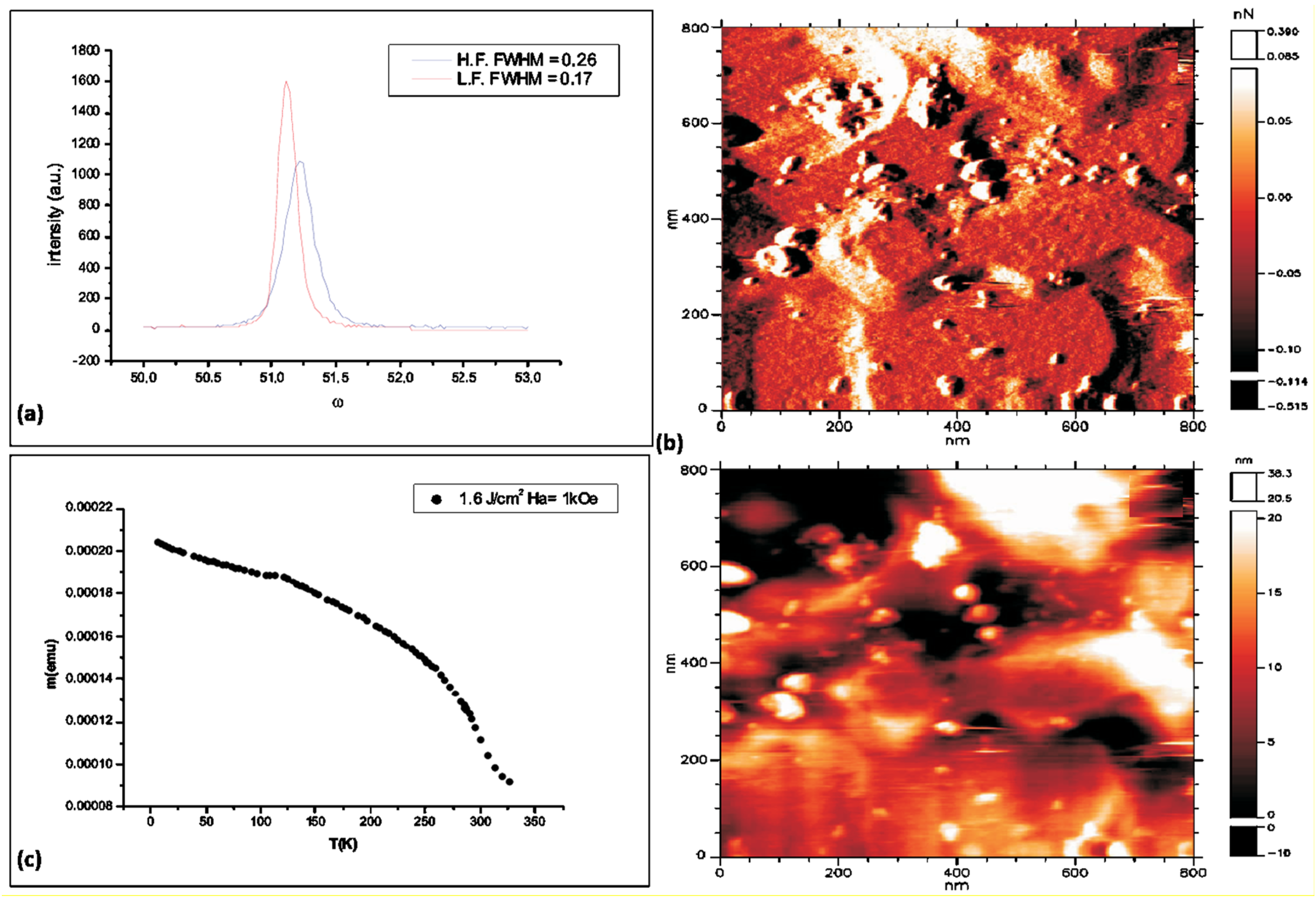
The SFMO investigated here were grown on STO substrates by PLD using a Nd:yttrium-aluminum-garnet (YAG) laser operating at 532 nm, with a pulse energy of 200 mJ and a pulse duration of 10 ns [95]. The substrate was placed at a distance of 5 cm from the target and heated at a temperature of 900 °C. The oxygen pressure in the PLD chamber was of 10−5 mbar. The regular crystallographic structure of the deposited films, having a thickness in the range 200–400 nm, was confirmed by x-ray analysis: θθ X-ray diffraction patterns and rocking curve analysis (typical values of the curve width was about 0.2°, as shown in Figure 2a). Moreover, a polycrystalline growth was confirmed by atomic force microscope (AFM) investigations, indicating the presence of some superficial nonordered clusters (see Figure 2b for details). The polycrystalline nature of the samples strongly influences the magnetic behavior, characterized by a ferromagnetic–paramagnetic transition with a Curie temperature K (see the - curves in Figure 2c).
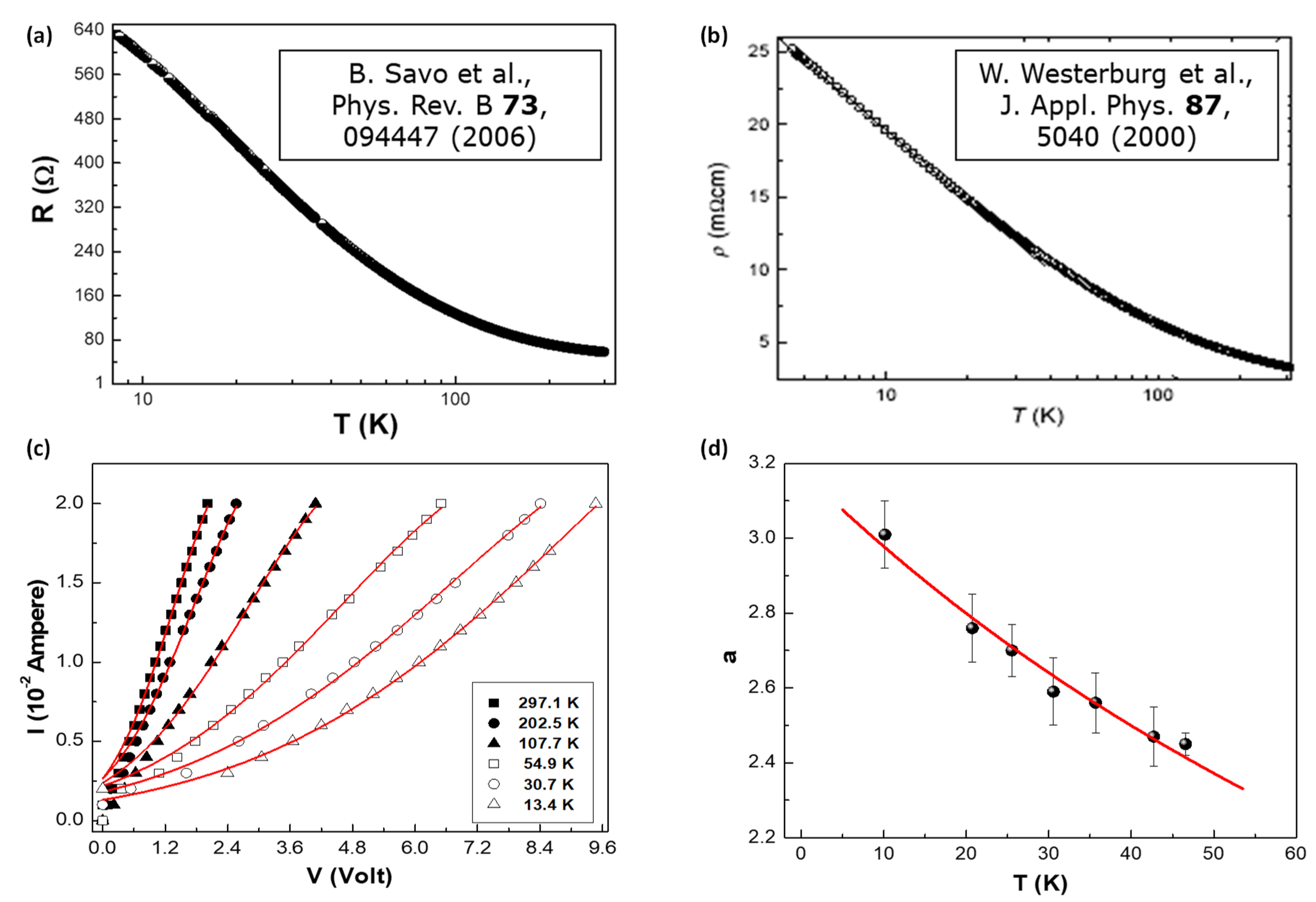
Semiconducting-like curves have been measured in polycrystalline samples (Figure 3a), obtaining results very similar to those already reported in literature for granular SFMO compounds (Figure 3b) [96]. In this respect, the fluctuation-induced tunneling (FIT) model has also been used to explain the electrical transport properties [56,97]. According to this model, the electrons, delocalized in large conducting segments (grains), tend to tunnel between these grains at the points of their closest approach, view as insulating gaps [98]. The large thermally activated voltage fluctuations across the junction influence the tunneling probability, resulting in non-Ohmic conductivity with a voltage dependence of the current given by:
where is a preexponential factor, and is a characteristic voltage. The parameter is temperature-dependent and can be expressed as:
with and being two specific temperatures related to the system under test [98]. Equation (1) has been used to fit the set of - curves, obtained at different temperatures, taking , , and as free fitting coefficients. As a result, a good agreement over the full voltage range (except at very low values) is observed, especially below 55 K, with A and V, and is shown in Figure 3c. In addition, has a temperature dependence which is well reproduced by Equation (2) below 55 K, with K and K (see Figure 3d for details). In the temperature region up to 55 K it is, therefore, quite evident that intergranular tunneling processes dominate the electrical transport properties of SFMO granular films.
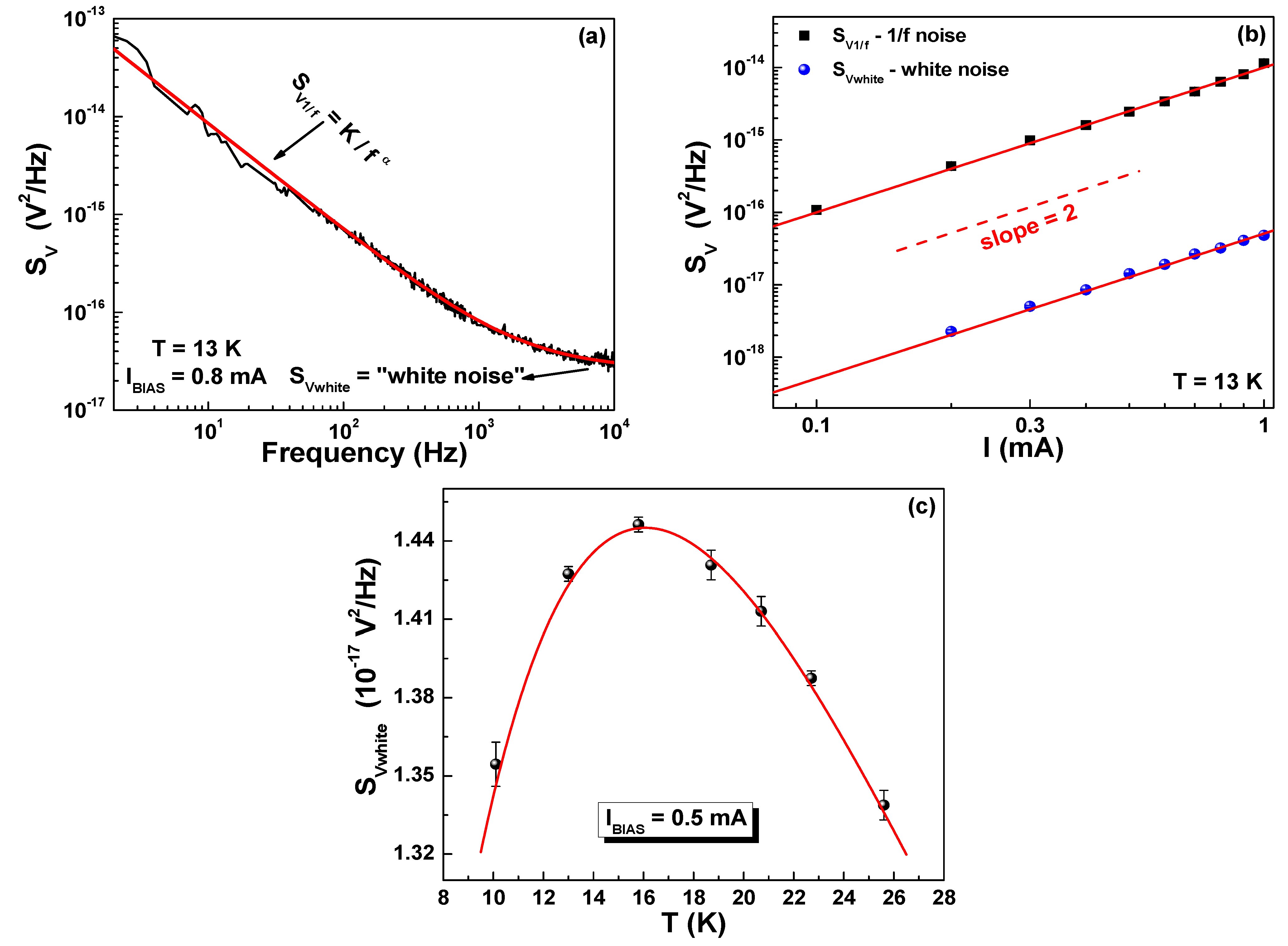
More difficult to understand, instead, is the high-temperature behavior where, as already observed in the case of carbon nanotube composites [44,45], fluctuation induced tunneling and thermal activation have to be considered as two parallel conduction mechanisms [98]. In this situation, dc electrical transport measurements alone are not able to clearly distinguish between FIT and thermal activation. Here voltage-noise investigations can be very useful for a better comprehension of the carriers dynamics. By analyzing the frequency dependence of the spectral density of voltage fluctuations in SFMO polycrystalline thin films, two distinct noise components are visible. A first component of 1/-type is found at low frequencies, while a constant amplitude spectrum (“white noise”) appears at higher frequencies, see Figure 4a. The quadratic bias current dependence of 1/ noise, shown as black squares in Figure 4b, is commonly expected for resistance fluctuations [29]. Conversely, the unexpected parabolic dependence of the “white noise” contribution, blue circles in Figure 4b, cannot be explained in terms of standard models. From the FIT conductivity, it is possible to define the frequency-independent conductance fluctuations, whose spectral density is proportional to and has a temperature dependence expressed as:
where is a preexponential factor. and are the same parameters of Equation (2) [56].
Figure 4c shows the experimental temperature dependence of the “white noise” for another set of SFMO samples, with a different configuration of the contact pads and measured at a dc current of 0.5 mA. The solid line is the best fit using Equation (3) with values of V2·K·Hz−1, K, and K, similar to those derived from Equation (2) in the context of dc transport. The agreement of the fitting expression with the experimental data in Figure 4c gives a strong indication on the validity of the FIT model in describing the transport and noise properties of SFMO polycrystalline thin films.
4.2. Current-Resistance Effects in La1−xSrxMnO3 Ultrathin Films
The influence of the electric field or the electric current on conductance (electric-resistance effect or current-resistance effect, respectively) has been widely observed on several CMR materials, and also in absence of an external magnetic field. In particular, a remarkable decrease of the peak resistance value due to the applied electric field has been found in La0.7Ca0.3MnO3/PbZr0.2Ti0.8O3 heterostructure at the metal-insulator transition temperature [99]. A similar decrease in the peak resistance, caused by an increased dc current, has been observed in La0.7Ca0.3MnO3 and La0.85Ba0.15MnO3 epitaxial thin films [100]. Moreover, current-dependent and hysteretic resistance behaviors have also been detected in quasi-one-dimensional nanopatterned phase-separated La0.67Sr0.33MnO3−δ thin films [101] and submicrometric constricted regions of La0.67Ba0.33MnO3−δ samples [102]. In order to explain these bias current effects, different hypotheses have been formulated, going from the strong interaction between carrier and Mn localized spins [100], to a percolative mechanism due to intrinsic phase separation [103,104], or to a local magnetic moment orientation by spin torque [102,105]. However, the characterizations of dc transport and magnetic properties alone were not able to clarify the nature of these peculiar aspects. Therefore, triggered by this situation and with the aim of obtaining useful information using the sensitive noise spectroscopy technique, an accurate experimental investigation of the charge carriers fluctuation mechanisms has been performed in LSMO ultrathin films, which are characterized by a strongly nonlinear resistance behavior.
LSMO ultrathin films, with a thickness ranging from 3.5 to 40 nm, were grown with MBE deposition on STO substrates, with the subsequent parameters: Deposition rate ~0.1 Å/s, substrate temperature ~850 °C, and oxygen pressure (a mixture of O2 + 5% ozone) of ≈ 8.5 × 10⁻⁵ Torr [57]. Reflected high-energy electron diffraction (RHEED) analysis, performed during the film deposition process, indicated an epitaxial growth. Ex situ X-ray diffraction (XRD) analysis confirmed the high crystallographic quality of all the films with very narrow rocking curves [106,107]. In order to estimate the surface roughness, an atomic force microscopy study was also carried out. A typical value of 0.5 nm for root-mean-square (RMS) roughness was observed on a scanning area of 1 μm2, in agreement with XRD low-angle-reflectivity measurements.
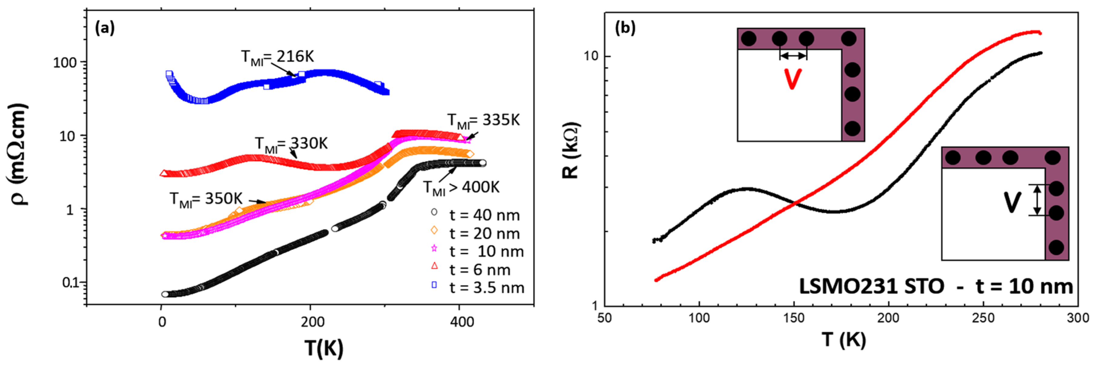
Since the investigated samples span over a wide range of thicknesses, a detailed analysis of the resistivity temperature dependence has been made, and the results are shown in Figure 5a, indicating the existence of a high metal-insulator transition temperature for nm. For the thinnest films ( nm), an in-plane anisotropy is evident in the curves. In fact, one configuration (top inset and red curve in Figure 5b) shows a standard behavior in the whole temperature range. Conversely, in the other configuration (right inset and black curve in Figure 5b), a low-temperature resistance peak occurs at K. Similar electric transport properties were found in the case of a meander line passing through 18 biepitaxial junctions in manganite thin films, where the presence of zones with reduced Curie temperatures (that is, paramagnetic/ferromagnetic junctions) was considered [108]. The low-temperature peak is explained as being induced by the ferromagnetic transition of these zones with reduced Curie temperatures [109,110].
The unusual behavior observed for the resistivity is equally reflected in the measurements, which are characterized by typical aspects of nonlinearity, more evident by increasing the bias current. This is clearly shown in Figure 6a for temperatures from 10 to 250 K, where the presence of a temperature-dependent threshold current, from an Ohmic to a non-Ohmic regime, is also visible. A theoretical picture, capable of capturing many of the experimental results, is the one which takes into account the presence of terraces on the surface of LSMO grown on STO substrates. This type of growth structure gives origin to the formation of step-edge regions, with high resistivity, between sample and substrate [111]. The in-plane anisotropy is produced by the flow of the bias current through such high-resistive zones, that are also zones of reduced Curie temperature [107]. The influence of polarized carriers on the magnetization values and on the height of the barriers of these regions adjacent to the terrace edges determines the characteristic non-Ohmic (or current-resistance) effect reported in Figure 6a [57].
A strong experimental support of the proposed interpretation is obtained with voltage-noise analysis. In particular, it is expected that changes in the configurations of impurities, eventually present in the barrier zones at the terrace edges, correspond to two different state levels, occupied by groups of atoms, whose energy can be represented in the form of two potential wells separated by a barrier. In general, the wells are asymmetric and the energies of their minima differ by some value. The atoms can tunnel from one well to the other, with a transition rate determined by interaction with phonons (in insulating solids) or with electrons (in conducting solids). This model is known as the two-level tunneling systems (TLTS), whose noise spectral density is characterized by the occurrence of a Lorentzian-type spectrum with a 1/ frequency dependence [29]. More in detail, if is the minimum relaxation time of such processes, for frequencies the main contribution to the spectral density is given by the 1/ component (, green solid lines in Figure 6b), while for frequencies the spectral density acquires the form:
where is the amplitude of Lorentzian noise (blue solid lines in Figure 6b). This corresponds to what was found in the investigated LSMO ultrathin films and shown in Figure 6b, in agreement with the prediction of the theoretical framework. Moreover, while in the Ohmic regime, the parabolic current dependence of the voltage-noise amplitude is explained in terms of standard resistance fluctuations inducing 1/ noise, in the non-Ohmic region, the observed scaling of the noise level with the bias current, significantly higher than the expected one, can be due to a current redistribution in a percolative system [57]. In this respect, additional studies on samples patterned with a controlled geometry would be necessary.
4.3. Spin Torque Effect in Differently Deposited La0.7Ba0.3MnO3 Thin Films
The colossal magnetoresistance phenomenon in half-metal oxide manganite compounds has been intensively studied over the past years and, as stated before, is explained within the framework of DE model. This DE mechanism qualitatively describes the metallic behavior of manganites in the ferromagnetic state, where Mn ions have aligned spins, and in the insulating regime above the Curie temperature, where Mn ions are characterized by randomly aligned spins, and their large magnetoresistance, due to field induced spin alignment. Even based on such an elementary DE picture, it is clear that the Mn–O–Mn structural arrangement plays a key role in determining magnetic and transport properties in manganite systems [112,113]. As stated in [114], in epitaxial thin films, this Mn–O–Mn arrangement can be also influenced by possible strain mechanisms due to lattice mismatch between film and substrate. As a matter of fact, it is widely reported that strained thin films usually show properties different from those of bulk compounds. In most cases, strain effects depress the ferromagnetic properties [115], but some results have also been reported showing ferromagnetism enhanced by tensile strain [116]. However, strain-less manganite films do not always reproduce bulk-like behavior.
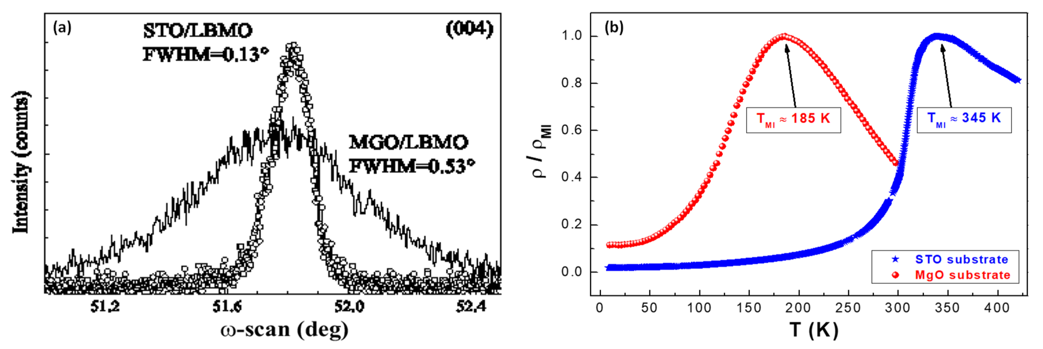
In order to get more information on these structural configurations and on their influence on electric and magnetotransport properties, a representative system to investigate is LBMO. In particular, a number of samples were deposited on (100) STO and (100) MgO substrates in a PLD chamber provided of a KrF excimer pulsed laser source ( = 248 nm). The films were fabricated starting from a LBMO stoichiometric target and using a typical energy density per laser shot of about 3 J/cm2, with a repetition rate of 3 Hz. The deposition was performed under a O2 + 5% O3 mixture pressure of 10−2 mbar and with the substrate temperature at 670 °C. Post-annealing processes in air were subsequently carried out by varying the temperature and the duration time [114]. These growth procedures resulted in a good in-plane matching between LBMO film and STO substrate, as indicated by standard XRD analysis, while substrate induced tensile strain seems to take place at the film/substrate interface in the MgO system. From rocking curve measurements, moreover, this significant difference between the two cases is also very evident. Indeed, as shown in Figure 7a, the full width at half maximum (FWHM) of rocking curve spectrum for MgO substrates is about four time larger than the FWHM for the film grown on STO. Similar values of the FWHM are found for LBMO samples on MgO at several (00) reflections, independently from the -index. This is expected when the largest contribution to the rocking curve broadening comes from mosaic spread of crystalline domains. All other sources of disorder in the investigated LBMO films on MgO substrates, such as domains size, granularity, and morphology, seem to be masked by this very large mosaicity [105].
Differences in the behaviors of the two systems (STO and MgO substrates) are also evidenced in the temperature dependence of the resistivity ratio , shown in Figure 7b. Two metal-insulator transition temperatures are observed and are characterized by corresponding resistivity values , different by about one order of magnitude. The experimental data in Figure 7b can be generally interpreted in terms of a model which predicts a competition between a ferromagnetic metallic (FM) and a paramagnetic insulating (PI) phase [105,114]. Within such a theoretical framework, for temperatures the transport properties are typically described in terms of polaronic conduction [117,118,119], instead at , in the FM region, the electrical conduction is related to different scattering processes, and the resistivity can be fitted with a generic -power law [106]. In the case of LBMO samples deposited on MgO substrate, however, the transition between the two regimes cannot be simply described using a superimposition of the FM and PI resistivities [105]. In fact, the FM phase also presents a resistivity that is not trivially correlated to a single scattering mechanism, while several processes, along with extrinsic-like percolative effects, are probably simultaneously at work. Therefore, more complicated conduction properties have to be considered for LBMO thin films grown on MgO substrates. This is furtherly confirmed by a low-temperature resistivity upturn for MgO substrate (red circles in Figure 7b), which gives an indication on the occurrence of localization phenomena and non-trivial mechanisms below .
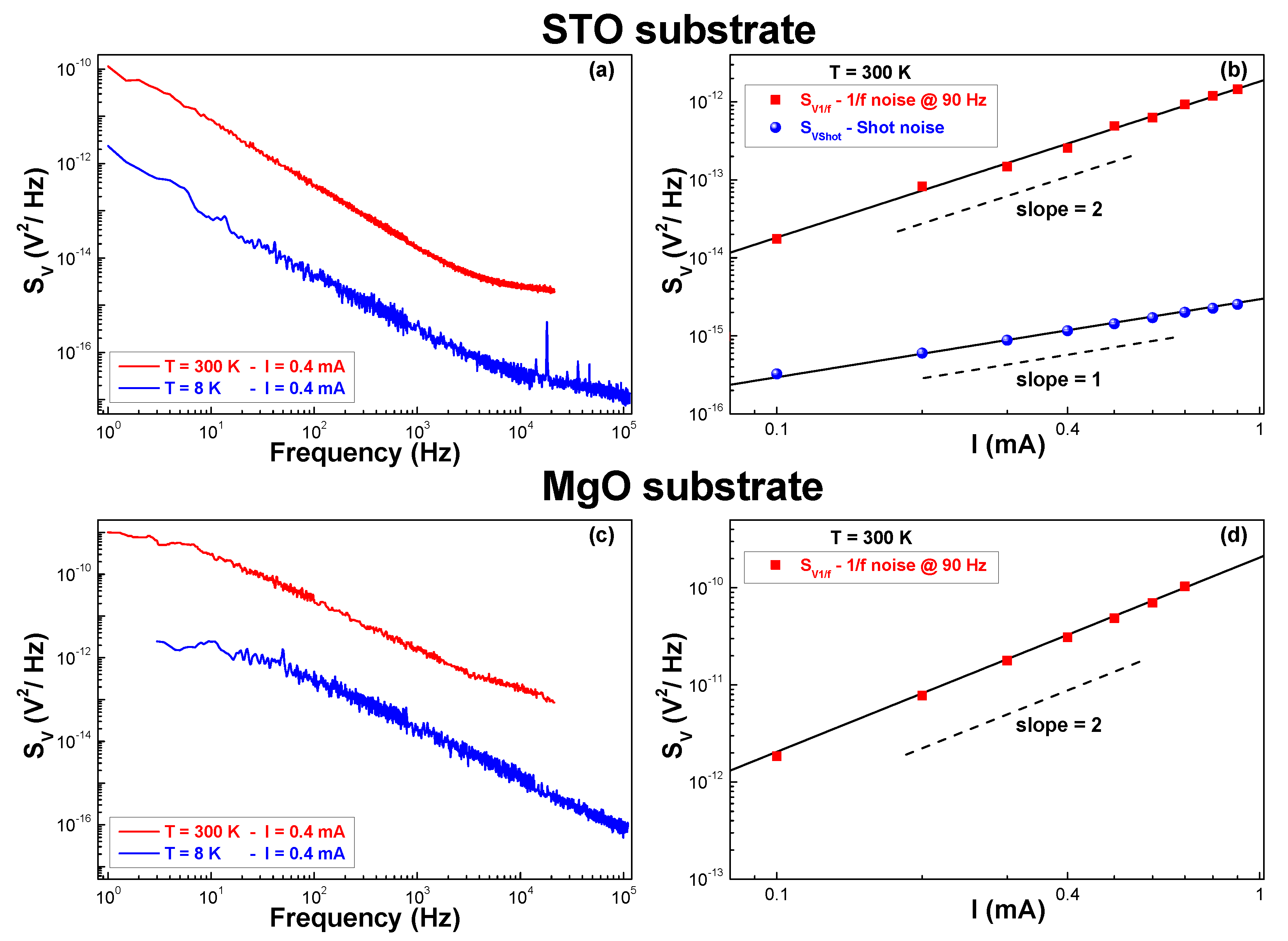
The identification of these peculiar charge carrier processes can be obtained by an analysis of the electric noise in function of external parameters, such as temperature and bias current. Figure 8a shows the measured voltage-spectral traces at a constant bias level of 0.4 mA in the case of STO substrate at two temperatures of 300 (red curve) and 8 K (blue curve), respectively. Two noise components can be identified, the first of 1/-type and the second frequency-independent. While , estimated at the frequency of 90 Hz, scales with the squared bias current (red squares in Figure 8b) and, therefore, is originated by resistance fluctuation mechanisms, is a linear function of the current (blue circles in Figure 8b) and can be associated with current fluctuation processes (shot noise).
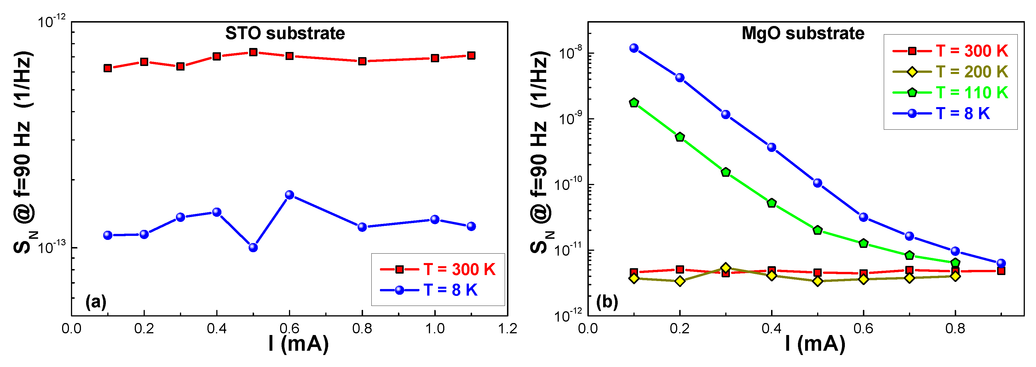
Whether the change in the LBMO film fabrication has a direct influence on the noise behavior can be verified by performing a voltage-spectral density analysis in the case of MgO substrate. Here, only a 1/ contribution is evident, as shown in Figure 8c in the whole investigated temperature range, thus representing a first difference from the STO case, although a quadratic bias current scaling is still preserved (Figure 8d, for details). This latter property could be interpreted, in principle, as due to resistance fluctuations, but a detailed study of the normalized spectral density , where is the voltage drop across the sample, provides different indications. Indeed, as widely reported in the scientific literature for Ohmic compounds, has to be current-independent in case of standard resistance fluctuation mechanisms [29,120,121], as indeed occurs for STO substrates both at room temperature (red squares) and at 8 K (blue circles), as shown in Figure 9a. Conversely, for LBMO films deposited on MgO substrates, is characterized by two distinct behaviors: An independence on the bias current above the metal-insulator transition (red squares and yellow diamonds in Figure 9b) and a reduction of noise with increasing bias at (green pentagons and blue circles in Figure 9b). In this low-temperature region, the explanation of the fluctuation processes cannot be based on the nature of the scattering centers due to the presence of mobile defects, as commonly found in metals and half-metals in a large number of experiments [29]. An improvement of the LBMO metallicity with the application of a larger and larger current needs to be considered. This enhanced ordering, appearing below the metal-insulator transition, seems to be strictly related to the magnetic behavior induced by the LBMO growth on MgO substrates.
In order to give a qualitative explanation of the experimental findings, it is important to consider, as widely reported in the scientific literature, the role played by the lattice mismatch between film and substrate in the magnetic and conduction mechanisms at work in manganite systems [112,113,115,116]. In particular, for LBMO on STO, the perfect in-plane matching between film and substrate characterizes the good metallicity of the samples [114]. Moreover, the absence of any type of strain effects reflects on the absence of unusual fluctuation processes and, consequently, usual resistance and current fluctuations are observed. Compared to this standard behavior, instead, anomalous conducting properties are clearly evident in the MgO case, where a large in-plane epitaxial mismatch at the film/substrate interface is identified [105]. Here, the presence of point defects and dislocations may lead to a system formed by bulklike domains separated by punctual defects and/or structural dislocations. In proximity of these, the manganite film experiences very complex strain mechanisms, giving rise to few nm-wide regions characterized by depleted conducting and magnetic properties (for example, depressed Curie temperatures) which can possibly result in super-paramagnetic (SP) behaviors. These smaller regions described in terms of SP clusters are characterized by a specific response to an external magnetic field [122], and could be partially aligned by a spin-polarized current which exerts a torque on the local magnetic domains. This is known as the spin torque effect [102,123], which is more evident below the metal-insulator transition producing an improvement of the system metallicity with the bias current. On the contrary, above the metal-insulator transition, this spin torque effect is less important and a conduction standard behavior prevails [58].
4.4. Charge Density Waves Conduction in Pr0.7Ca0.3MnO3 Epitaxial Thin Films
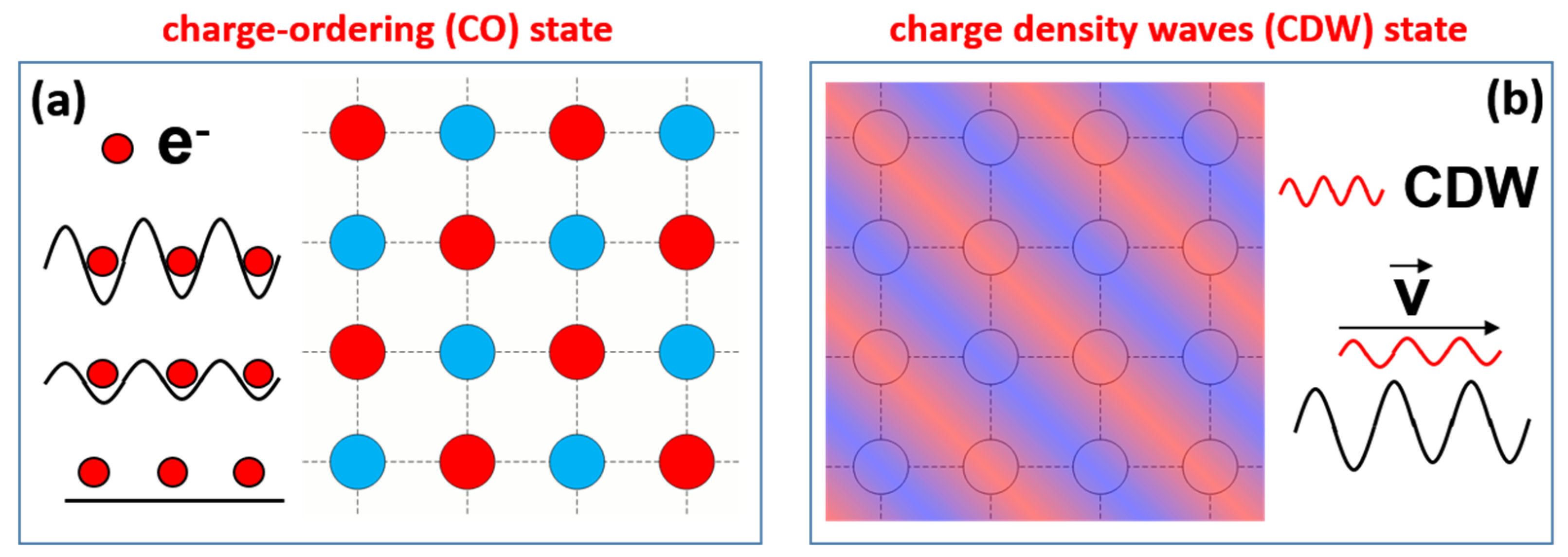
The earlier scientific literature ascribed many peculiar effects of mixed-valence perovskitic manganites to the destruction of a charge-ordering (CO) state, that is a strong charge localization on a single ion site [124,125,126]. The process of inducing conduction into a CO state can be realized with the application of external perturbations, such as electric or magnetic fields (see the scheme in Figure 10a). This classical interpretation of the melting of the CO phase has been recently challenged by several authors, resorting to a picture based on the existence of a CDW state where the charge modulation is weakly coupled with lattice [127,128,129,130]. In this framework, a collective transport of charge density waves can be induced by the application of an external electric field, giving rise to the well-known mechanism of sliding CDW (see the scheme in Figure 10b). The debate is still on nowadays, as evidenced in two recent papers [131,132] where the observation of negative differential resistance, specifically abrupt resistance increases at critical voltages in the characteristics, supports the electric phase separation scenario. Therefore, a systematic study of the electric noise properties could be very indicative in favor of one interpretation with respect to the other.
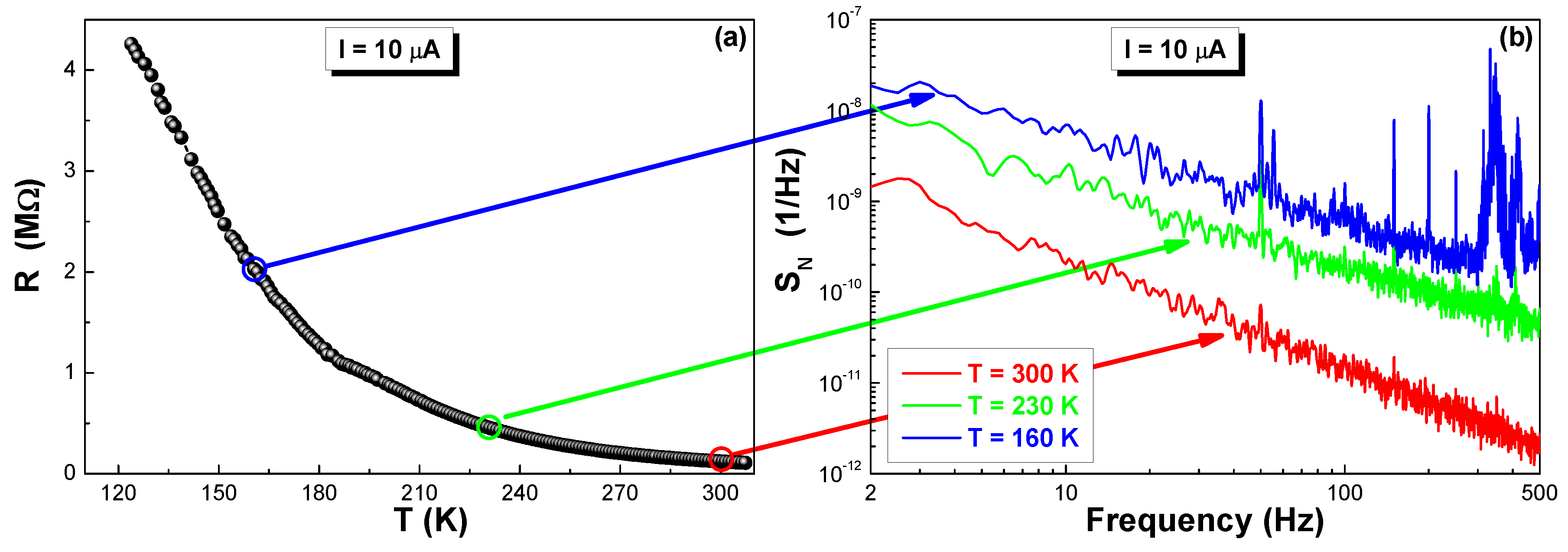
In order to have adequate samples for the planned experimental investigations, PCMO ultrathin films (10-nm-thick) were fabricated by PLD technique on (100) STO substrates. The deposition parameters, reported elsewhere [133], were optimized to obtain an epitaxial growth and a high crystal quality of PCMO. Moreover, flat surfaces (two-dimensional growth) and a tetragonal unit cell were also evidenced by performing detailed structural analyses, such as reflection high-energy electron diffraction (RHEED) and reciprocal space map (RSM). On this type of high-quality samples by choosing a critical Ca doping value of , it is very common to observe in the phase diagram a borderline behavior with a transition to a glassy ferromagnetism below 120 K and a charge modulation transition at about 230 K [134,135]. While no evidence of such a peculiar behavior appears in the curves (see Figure 11a), a clear variation is found, instead, in the noise level (see the green and blue normalized voltage-spectral traces in Figure 11b). This confirms the sensitivity of the electronic noise to charge modulated states in narrow-band manganites [128,136].
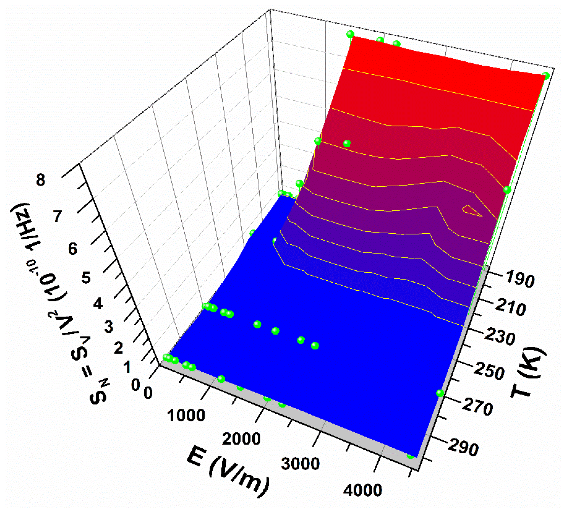
In particular, the normalized voltage-noise reveals a unique 1/ component between 160 and 300 K, as shown in Figure 11b, whose amplitude is characterized by a step-like increase of more than one order of magnitude at 230 K (see the three-dimensional plot in Figure 12). Below 230 K, the same Figure 12 shows the existence of a threshold electric field ( ~ 1000 V/m) above which a high noise intensity is observed.
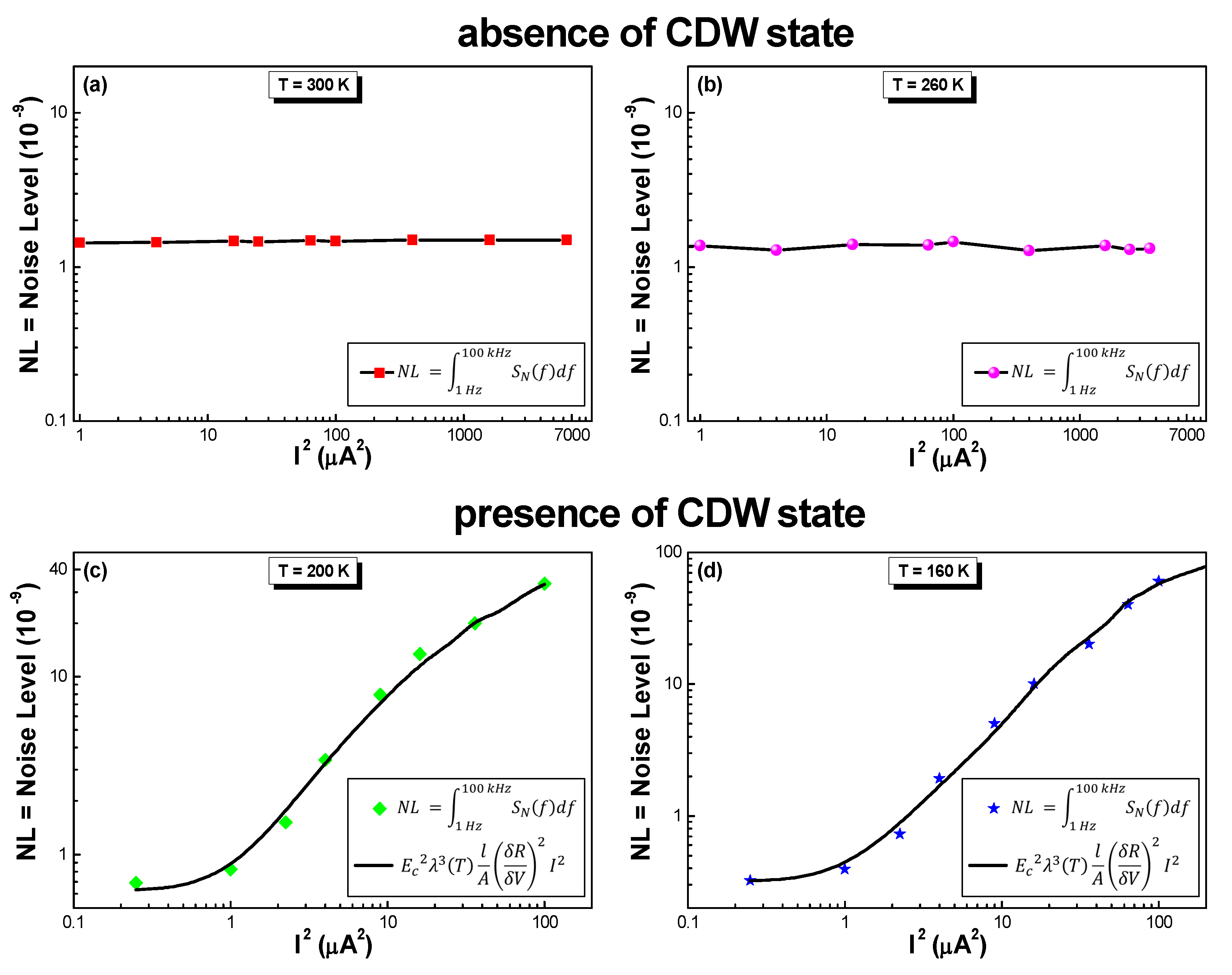
The observed step-like noise increase and its dependence on the electric field are not easy to reconcile with a strong coupling, charge localized melting scenario. The continuity of at the CO transition temperature and the presence of broadband 1/ noise, arising below CO transition, can be understood, instead, in a CDW state in the framework of a two-fluid model. The sliding of the CDWs, moreover, is responsible for the noise enhancement above [59]. The validity of the proposed interpretation is obtained by comparing the experimental noise level data with the quantitative predictions verified on conventional CDW systems. According to [137], the nonlinear conductance, which is a typical signature of CDW states, is strictly related with by considering the pinning force fluctuations as the source of noise in the chordal resistance . The expression extracted from theoretical calculations, and adapted from [137], can be written as:
where 1 Hz–100 kHz is the frequency bandwidth of measurement, the fitting parameter is the pinning coherence length, and are the sample length and area, respectively, and establishes the quantitative relation between the nonlinear conductance and the noise level. Equation (5) can be used to identify the occurrence of a CDW state, starting from electric noise measurements. Indeed, as shown in Figure 13a at 300 K and in Figure 13b at 260 K, is independent on and, therefore, Equation (5) cannot be applied. This gives the direct indication about the absence of a CDW state, as expected above the CO transition [127,128]. Conversely, the good agreement between the model reproduced with Equation (5) and the noise data at 200 K (see Figure 13c) and at 160 K (see Figure 13d) is a clear signature of the presence of a CDW state below the CO transition temperature (230 K). More in detail, the best fitting procedure through Equation (5) allows us to determine the coherence volume , that is the typical volume over which the CDW phase is deformed in going from one metastable state to another [137]. A value of m3 is evaluated at 160 K, close to the Lee-Rice coherence volume ( m3) characteristic of CDW systems [138]. Moreover, a strong decrease in m3 is observed at 200 K, still consistently with the Lee-Rice result that when the CO transition is approached [138].
Overall, the theoretical interpretation of CDWs establishment in manganites is supported by the investigation of the electric noise processes. The results obtained with the analysis of the experimental data suggest that the CDW mechanism should be introduced as one of the bricks necessary to build up the comprehension of strongly correlated transition-metal oxides. In this context, a direct consequence of introducing the CDW dynamics to describe the electric transport of perovskite compounds is that the understanding of correlated oxide properties should be pursued in the broader context of complexity [139].
4.5. Weak-Localization and Quantum Interference Effects in Manganites
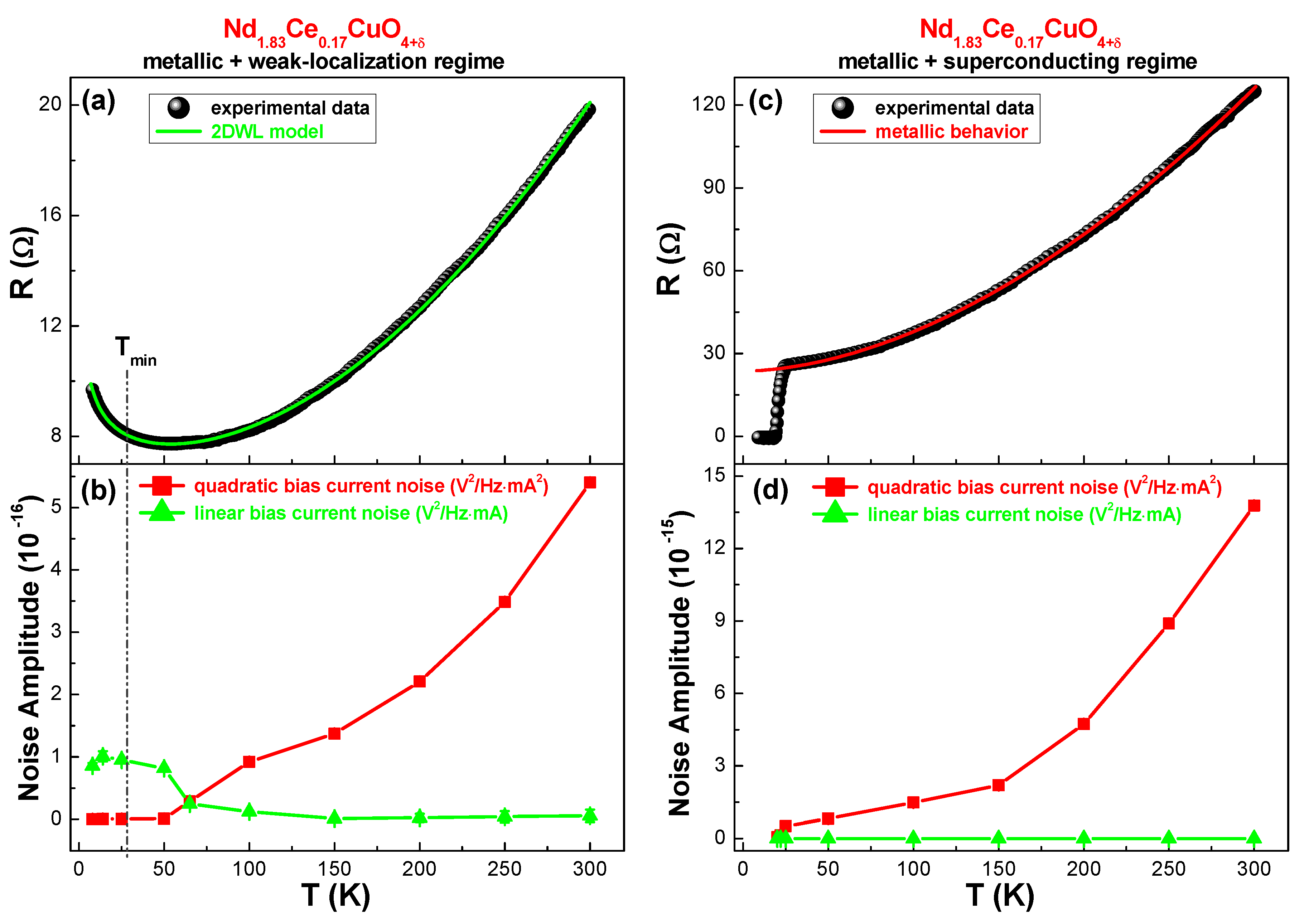
QIEs often influence low-temperature electrical conduction in a disordered metal [140]. Among the most fascinating and intriguing features related to these effects there are, undoubtedly, WL and universal conductance fluctuations (UCFs), whose direct connection, up to now, has been proposed, but never demonstrated. Previous works have shown that electron-doped Nd1.83Ce0.17CuO4+δ (NCCO) thin films can have an upturn of resistivity at low temperatures, attributed to WL phenomena due to excess oxygen ions randomly distributed in the lattice structure [141,142]. In these compounds, a preliminary study has revealed that WL (Figure 14a) is related to an unusual noise-spectral density of 1/-type. According to Hooge empirical relation, the noise amplitude should scale with the square of the dc bias current. This behavior is found in many materials, where the noise is essentially related to random resistance fluctuations. In the case of NCCO, in the WL regime, the measured 1/ noise shows a very weak temperature dependence and a peculiar linear bias current scaling of the spectral density (green triangles in Figure 14b). At temperatures above the WL transition or in metallic NCCO samples (Figure 14c), the standard resistance fluctuation behavior, with a quadratic bias current noise dependence, is gradually recovered (red squares in Figure 14d).
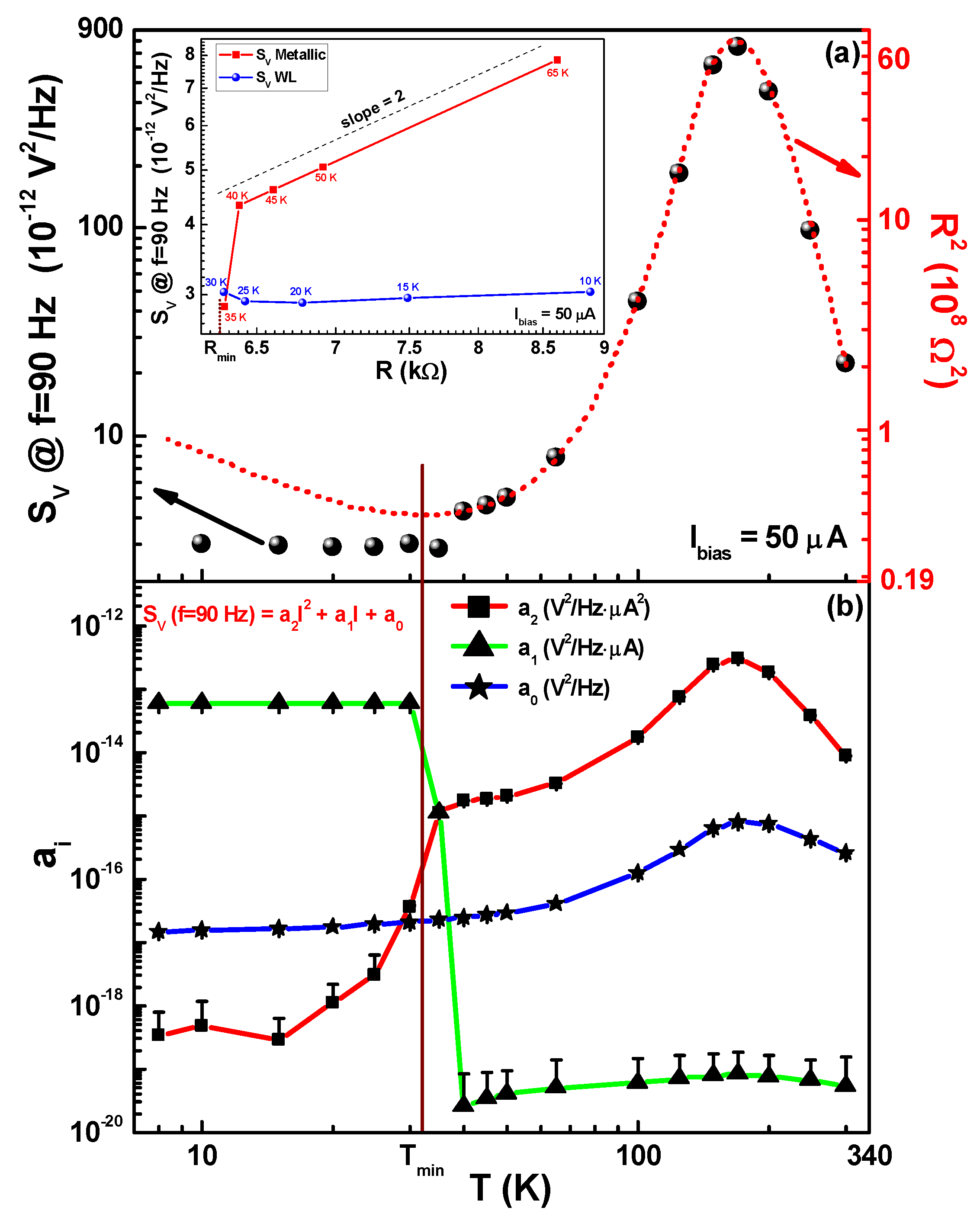
Natural candidates for the realization of experiments useful to clarify these aspects are manganese oxides, which are expected to show QIEs due to UCFs and, under well controlled fabrication conditions, exhibit WL at relatively high temperatures (i.e., K). Therefore, a detailed noise analysis have been performed on LBMO thin films deposited onto STO substrates by using low oxygen pressure (10−2 mbar) and low laser fluence (pulse energy of 25 mJ). While samples deposited at high fluence (200 mJ) are characterized by optimal transfer of target stoichiometry to the film and by an ordered microstructure, the samples under consideration are characterized by heavy ion (La, Ba) deficiency and by a disordered microstructure. In such a disordered manganite system, WL phenomena are found to occur below a crossover temperature K, signaling a resistance upturn as shown by the red dashed line in Figure 15a [114,143,144]. Here, the temperature dependence of , estimated at a reference frequency of 90 Hz, is also reported as black points. At a fixed bias current (the data refer to a value of 50 μA), the standard theory of resistance fluctuations in Ohmic compounds implies that [29]. Both quantities are shown in Figure 15a, with a very good agreement for temperatures above . This suggests the existence of a standard noise process, essentially due to resistance fluctuations, at high temperatures. Conversely, Figure 15a shows that such a model is not applicable below , where QIEs appear, producing an upturn of the resistivity. Limiting the noise analysis in a range close to , estimated at comparable resistance values is higher in the metallic side than in the WL side. In particular, the blue data points in the inset to Figure 15a show no specific resistance dependence, indicating explicitly that another type of 1/ noise is activated below with unusual properties. These unconventional characteristics of the 1/ component are better evidenced by the bias current dependence of the noise spectral density, and can be analyzed using a fitting procedure with a general quadratic function of the form: in the whole investigated temperature range. Above , the quadratic coefficient is clearly the dominant term (squares and red line in Figure 15b), thus confirming that electric noise is originated by resistance fluctuations, with a squared current dependence as the distinctive feature [29]. The parameter is strongly suppressed in the crossing from metallic to WL regime, while a new noise contribution, linear in bias current and proportional to , arises (triangles and green line in Figure 15b). The coefficient (stars and blue line in Figure 15b) originates from frequency-independent noise contributions and matches well with the temperature dependence of the sample Johnson noise. This is the same result obtained in non-superconducting NCCO thin films undergoing WL transition, shown in Figure 14a, indicating, therefore, a strong connection between anomalous fluctuation mechanisms and QIEs, highly reproducible in different samples and materials.
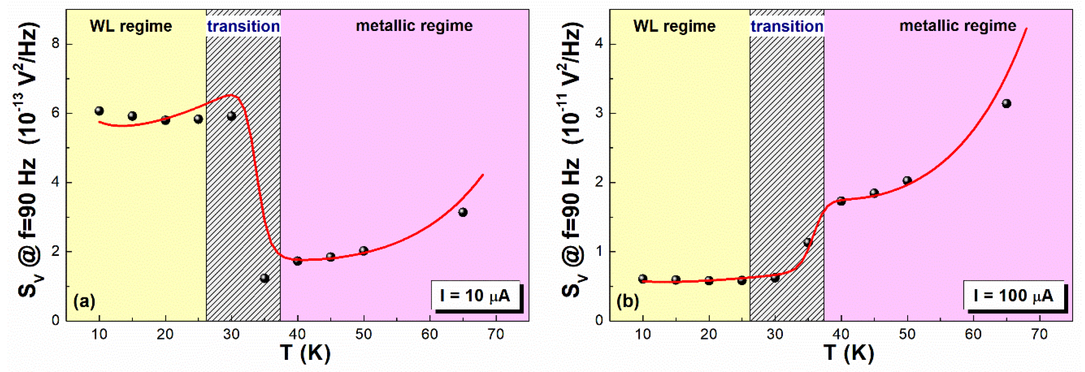
In order to validate the close link between WL and unconventional 1/ noise, an appropriate theoretical interpretation is necessary. In this respect, a simple model based on non-equilibrium UCFs has been developed, suggesting that in disordered systems, the low-temperature noise () is mainly originated by the dephasing of the electronic paths, while above standard thermal averaging can fully explain the observed noise. This framework leads to an explicit dependence of the voltage-spectral density on the bias current as:
where is the Boltzmann constant, is the electron charge, and is a dimensionless scaling parameter [60,145]. From a qualitative point of view, Equation (6) establishes that, in disordered thin films of characteristic size and at low temperatures, the phase coherence of the sample over regions of typical size induces a new source of noise based on the UCFs phenomenology. In this quantum-like regime, the time-dependent conductance fluctuations are produced by the dephasing of the electrons paths, the latter being at the origin of unconventional 1/ fluctuations. In this picture, the bias current not only probes the conductance changes, as expected for , but actively participates in the dephasing-driven noise dynamics. This interpretation is supported by a substantial lowering of the noise level in the WL regime, which can be explained by a saturation effect of the conductance fluctuations. At finite temperature, the sample is ideally divided in regions of typical size within which coherence effects are relevant. The motion of impurities inside these coherent subsystems produces additive changes of the conductance as long as the total variance (i.e., the total noise amplitude) is saturated to the universal value , being the conductance of a single coherent subsystem [60]. The microscopic mechanism described above substantially limits the noise level and qualitatively explains the saturation behavior detected in WL regime (see the low-temperature data points in Figure 15a). Even though universal behavior of UCFs is expected only in equilibrium condition and zero temperature (i.e., for a fully coherent sample), in our case, some relics of this universal behavior could be present for . The agreement between theory and experiment is confirmed by the red solid curves of Figure 16, obtained by a best fitting procedure of Equation (6). The model prediction is appreciable both at a fixed bias current value of 10 μA (Figure 16a) and at 100 μA (Figure 16b), slightly deviating from the experimental data points only in the transition region around . These findings demonstrate the direct connection between WL and UCFs and, consequently, the relation of 1/ noise with quantum nature of matter at the boundary between classical and quantum realm. Further studies, however, are required to better understand the origin of low-temperature unconventional noise in systems whose microstructural disorder can be appropriately induced, such as, for example, nanowires and one-dimensional (1D) confined electron gases.
5. Comparison of Noise Properties
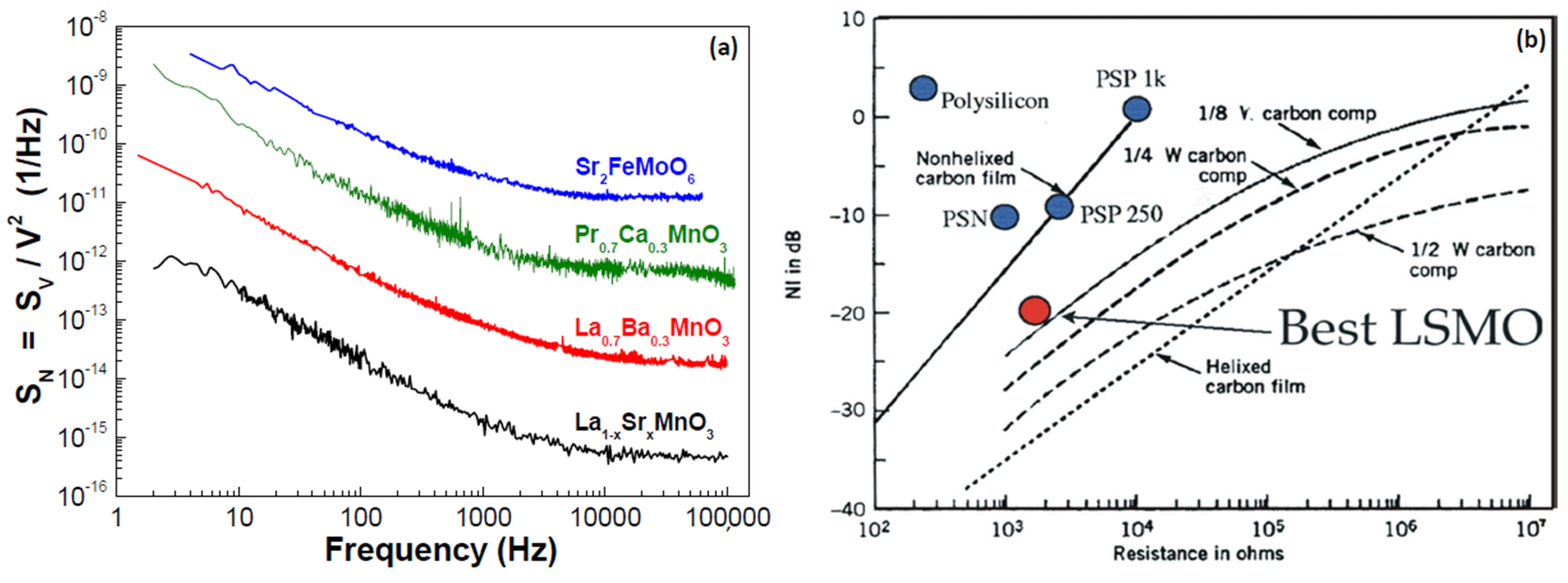
The experimental analyses reported here have shown the high potential of perovskitic magnetic compounds for applications as magnetoresistive devices, such as magnetic random access memories and sensors. Moreover, the large change of the resistance at the metal-insulator transition also makes these materials, in particular LBMO, good candidates for the fabrication of uncooled or moderately cooled bolometers. For all these industrial and/or commercial purposes, the study of electric noise is very important, and the evaluation of the noise level is necessary to identify the best material to use. As reported in Figure 17a, which shows the frequency dependence of the normalized voltage-spectral density (intrinsic noise level) of the investigated perovskitic compounds, LSMO epitaxial thin films have the lower noise level compared to other materials. These latter compounds, although useful in technological applications for their high Curie temperature values, need improvement of the deposition conditions in order to produce high-quality thin films.
The best LSMO studied here, fabricated by using both molecular beam epitaxy and pulsed laser deposition techniques, can be further compared with other metallic and polysilicon materials to extract additional information from a technological point of view. In this respect, Figure 17b, which reports the noise level calculated in decibels, shows very low noise and resistivity values for LSMO. This experimental evidence of intrinsic electric noise comparable or, in several cases, better than the one of standard and well-known metallic and semiconducting compounds, makes these manganese oxides promising for application in innovative and advanced electronic devices.
Author Contributions
All authors have contributed to the conceptualization, writing, review, and editing of the manuscript. All authors have read and agreed to the published version of the manuscript.
Funding
The authors acknowledge partial support from University of Salerno through grants 300391FRB17PAGAN, 300391FRB18CAVAL, and 300391FRB19PAGAN.
Data Availability Statement
The data presented in this study are not publicly available. Data are however available from the authors upon reasonable request and with permission of University of Salerno.
Acknowledgments
Salvatore Abate from CNR-SPIN Salerno (Italy) is gratefully acknowledged for his technical support.
Conflicts of Interest
The authors declare no conflict of interest.
CARLO BARONE
The author was born in Salerno, Italy, in 1976. From April 12, 2017, he has the Habilitation for Associate Professor in 02/B1 (Experimental Condensed Matter Physics). On February 29, 2008, he was awarded a Ph.D. in Physics (specialization Condensed Matter), at the University of Salerno. Most of his scientific activity has focused on the elaboration of stochastic signals originated by non-equilibrium processes in innovative materials and devices. Actually, he is a member of the Editorial Board of Scientific Reports. Moreover, he has been Coordinator and Principal Investigator of a national “Seed” Project entitled: “Is weak localization detected by 1/f noise?”, funded by the CNR-SPIN Institute (April, 2012 - February, 2013). From April 07, 2008 to August 31, 2019, he worked at the University of Salerno (Department of Physics) and at the Institute CNR-SPIN as Research Fellow. Nowadays, he is Senior Researcher at the Department of Physics (University of Salerno).
SERGIO PAGANO
The author was born in Salerno, Italy, in 1959. In 1984, he received a M.Sc degree (cum laude) in physics at the University of Salerno, and in 1987 a Ph.D. degree at the Technical University of Denmark. From 1987 to 2005, he was a researcher (senior researcher from 2001) at the Institute of Cybernetics of the C.N.R., Italy. In 2005, he became Associate Professor at the University of Salerno. Since 2019, he is a Full Professor of experimental physics at the University of Salerno. His research covers superconductive electronics and devices, cryogenic radiation detectors, noise spectroscopy, and nonlinear and complex systems. He has authored about 190 scientific publications.
References
- Coey, J.M.D.; Viret, M.; von Molnár, S. Mixed-valence manganites. Adv. Phys. 1999, 48, 167–293. [Google Scholar] [CrossRef]
- Dagotto, E.; Hotta, T.; Moreo, A. Colossal magnetoresistant materials: The key role of phase separation. Phys. Rep. 2001, 344, 1–153. [Google Scholar] [CrossRef] [Green Version]
- Gor’kov, L.P.; Kresin, V.Z. Mixed-valence manganites: Fundamentals and main properties. Phys. Rep. 2004, 400, 149–208. [Google Scholar] [CrossRef]
- Liang, L.; Li, L.; Wu, H.; Zhu, X. Research progress on electronic phase separation in low-dimensional perovskite manganite nanostructures. Nanoscale Res. Lett. 2014, 9, 325. [Google Scholar] [CrossRef] [PubMed] [Green Version]
- Gangopadhyay, S.; Pickett, W.E. Interplay between spin-orbit coupling and strong correlation effects: Comparison of the three osmate double perovskites Ba2AOsO6 (A = Na, Ca, Y). Phys. Rev. B 2016, 93, 155126. [Google Scholar] [CrossRef] [Green Version]
- Chapman, J.P.; Attfield, J.P.; Rodriguez-Martinez, L.M.; Lezama, L.; Rojo, T. Phase separation in manganites induced by orbital–ordering strains. Dalt. Trans. 2004, 3026–3031. [Google Scholar] [CrossRef]
- Li, N.; Fan, F.; Sun, F.; Wang, Y.; Zhao, Y.; Liu, F.; Zhang, Q.; Ikuta, D.; Xiao, Y.; Chow, P.; et al. Pressure-enhanced interplay between lattice, spin, and charge in the mixed perovskite La2FeMnO6. Phys. Rev. B 2019, 99, 195115. [Google Scholar] [CrossRef] [Green Version]
- Zurauskiene, N.; Rudokas, V.; Balevicius, S.; Kersulis, S.; Stankevic, V.; Vasiliauskas, R.; Plausinaitiene, V.; Vagner, M.; Lukose, R.; Skapas, M.; et al. Nanostructured La–Sr–Mn–Co–O films for room-temperature pulsed magnetic field sensors. IEEE Trans. Magn. 2017, 53, 4002605. [Google Scholar] [CrossRef]
- Xia, W.; Pei, Z.; Leng, K.; Zhu, X. Research progress in rare earth-doped perovskite manganite oxide nanostructures. Nanoscale Res. Lett. 2020, 15, 9. [Google Scholar] [CrossRef] [Green Version]
- Miclea, C.; Tanasoiu, C.; Miclea, C.F.; Tanasoiu, V. Advanced electroceramic materials for electrotechnical applications. J. Optoelectron. Adv. Mater. 2002, 4, 51–58. [Google Scholar]
- Levy, P.; Parisi, F.; Granja, L.; Indelicato, E.; Polla, G. Novel dynamical effects and persistent memory in phase separated manganites. Phys. Rev. Lett. 2002, 89, 137001. [Google Scholar] [CrossRef] [PubMed] [Green Version]
- Ghosh, N.; Datta, S.; Ghosh, B. Size dependence in magnetic memory, relaxation and interaction of La0.67Sr0.33MnO3. J. Magn. Magn. Mater. 2015, 382, 277–282. [Google Scholar] [CrossRef]
- Mlejnek, P.; Vopálenský, M.; Ripka, P. AMR current measurement device. Sens. Actuators A Phys. 2008, 141, 649–653. [Google Scholar] [CrossRef]
- Jogschies, L.; Klaas, D.; Kruppe, R.; Rittinger, J.; Taptimthong, P.; Wienecke, A.; Rissing, L.; Wurz, M.C. Recent developments of magnetoresistive sensors for industrial applications. Sensors 2015, 15, 28665–28689. [Google Scholar] [CrossRef] [PubMed] [Green Version]
- Jin, S.; Tiefel, T.H.; McCormack, M.; Fastnacht, R.A.; Ramesh, R.; Chen, L.H. Thousandfold change in resistivity in magnetoresistive La–Ca–Mn–O films. Science 1994, 264, 413–415. [Google Scholar] [CrossRef] [Green Version]
- Moritomo, Y.; Asamitsu, A.; Kuwahara, H.; Tokura, Y. Giant magnetoresistance of manganese oxides with a layered perovskite structure. Nature 1996, 380, 141–144. [Google Scholar] [CrossRef]
- Ota, S.; Ando, A.; Chiba, D. A flexible giant magnetoresistive device for sensing strain direction. Nat. Electron. 2018, 1, 124–129. [Google Scholar] [CrossRef]
- Guillet, B.; Méchin, L.; Yang, F.; Routoure, J.M.; Le Dem, G.; Gunther, C.; Robbes, D.; Chakalov, R.A. Net of YBCO and LSMO Thermometers for Bolometric Applications BT—Advanced Experimental Methods For Noise Research in Nanoscale Electronic Devices; Sikula, J., Levinshtein, M., Eds.; Springer: Dordrecht, The Netherlands, 2004; pp. 327–336. [Google Scholar]
- Méchin, L.; Perna, P.; Barone, C.; Routoure, J.M.; Simon, C. La0.7Sr0.3MnO3 thin films on Bi4Ti3O12/CeO2/yttria-stabilised-zirconia buffered Si(0 0 1) substrates: Electrical, magnetic and 1/f noise properties. Mater. Sci. Eng. B Solid State Mater. Adv. Technol. 2007, 144, 73–77. [Google Scholar]
- Méchin, L.; Perna, P.; Saïb, M.; Belmeguenai, M.; Flament, S.; Barone, C.; Routoure, J.-M.; Simon, C. Structural, 1/f noise and MOKE characterization of vicinal La0.7Sr0.3MnO3 thin films. Acta Phys. Pol. A 2007, 111, 63–70. [Google Scholar] [CrossRef]
- Fontcuberta, J.; Balcells, L.; Bibes, M.; Navarro, J.; Frontera, C.; Santiso, J.; Fraxedas, J.; Martínez, B.; Nadolski, S.; Wojcik, M.; et al. Magnetoresistive oxides: New developments and applications. J. Magn. Magn. Mater. 2002, 242–245, 98–104. [Google Scholar] [CrossRef]
- Dhital, C.; de la Cruz, C.; Opeil, C.; Treat, A.; Wang, K.F.; Liu, J.-M.; Ren, Z.F.; Wilson, S.D. Neutron scattering study of magnetic phase separation in nanocrystalline La5/8Ca3/8MnO3. Phys. Rev. B 2011, 84, 144401. [Google Scholar] [CrossRef] [Green Version]
- Reutler, P.; Bensaid, A.; Herbstritt, F.; Höfener, C.; Marx, A.; Gross, R. Local magnetic order in manganite thin films studied by 1/f noise measurements. Phys. Rev. B 2000, 62, 11619–11625. [Google Scholar] [CrossRef]
- Routoure, J.M.; Méchin, L.; Fadil, D.; Barone, C.; Mercone, S.; Perna, P.; Flament, S. Low frequency noise in La0.7Sr0.3MnO3 thin films: Effects of substrate materials and contact resistance. AIP Conf. Proc. 2007, 922, 229–232. [Google Scholar]
- Belogolovskii, M.; Jung, G.; Markovich, V.; Dolgin, B.; Wu, X.D.; Yuzhelevski, Y. Bias dependent 1/f conductivity fluctuations in low-doped La1−xCaxMnO3 manganite single crystals. J. Appl. Phys. 2011, 109, 73920. [Google Scholar] [CrossRef] [Green Version]
- Barone, C.; Pagano, S.; Méchin, L.; Guillet, B.; Routoure, J.-M. Comment on “A case study on the scaling of 1/f noise: La2/3Sr1/3MnO3 thin films. J. Appl. Phys. 2014, 115, 116101. [Google Scholar] [CrossRef]
- Przybytek, J.; Fink-Finowicki, J.; Puźniak, R.; Markovich, V.; Jung, G. Noise signatures of metastable resistivity states in ferromagnetic insulating manganite. J. Appl. Phys. 2015, 118, 043903. [Google Scholar] [CrossRef]
- Przybytek, J.; Fink-Finowicki, J.; Puźniak, R.; Shames, A.; Markovich, V.; Mogilyansky, D.; Jung, G. Robust random telegraph conductivity noise in single crystals of the ferromagnetic insulating manganite La0.86Ca0.14MnO3. Phys. Rev. B 2017, 95, 125101. [Google Scholar] [CrossRef]
- Kogan, S. Electronic Noise and Fluctuations in Solids; Cambridge University Press: Cambridge, UK, 1996; ISBN 9780521460347. [Google Scholar]
- Bendat, J.S.; Piersol, A.G. Random Data: Analysis and Measurement Procedures: Fourth Edition; Wiley Blackwell: Hoboken, NJ, USA, 2012; ISBN 9781118032428. [Google Scholar]
- Kiss, L.B.; Svedlindh, P. New Noise Exponents in random conductor-superconductor and conductor-insulator mixtures. Phys. Rev. Lett. 1993, 71, 2817–2820. [Google Scholar] [CrossRef]
- Galeazzi, M.; Zuo, F.; Chen, C.; Ursino, E. Intrinsic noise sources in superconductors near the transition temperature. Nucl. Instrum. Methods Phys. Res. Sect. A Accel. Spectrometersdetect. Assoc. Equip. 2004, 520, 344–347. [Google Scholar] [CrossRef]
- Barone, C.; Romeo, F.; Pagano, S.; Adamo, M.; Nappi, C.; Sarnelli, E.; Kurth, F.; Iida, K. Probing transport mechanisms of BaFe2As2 superconducting films and grain boundary junctions by noise spectroscopy. Sci. Rep. 2014, 4, 6163. [Google Scholar] [CrossRef] [Green Version]
- Barone, C.; Mauro, C.; Carapella, G.; Pagano, S. Comparison of the Electric Noise Properties of novel superconductive materials for electronics applications. IEEE Trans. Appl. Supercond. 2018, 28, 1100404. [Google Scholar] [CrossRef]
- Dantsker, E.; Tanaka, S.; Nilsson, P.-Å.; Kleiner, R.; Clarke, J. Reduction of 1/f noise in high-Tc dc superconducting quantum interference devices cooled in an ambient magnetic field. Appl. Phys. Lett. 1996, 69, 4099–4101. [Google Scholar] [CrossRef] [Green Version]
- Choi, S.; Lee, D.-H.; Louie, S.G.; Clarke, J. Localization of metal-induced gap states at the metal-insulator interface: Origin of flux noise in SQUIDs and superconducting qubits. Phys. Rev. Lett. 2009, 103, 197001. [Google Scholar] [CrossRef] [PubMed] [Green Version]
- Pagano, S.; Martucciello, N.; Enrico, E.; Monticone, E.; Iida, K.; Barone, C. Iron-based superconducting nanowires: Electric transport and voltage-noise properties. Nanomaterials 2020, 10, 862. [Google Scholar] [CrossRef] [PubMed]
- Barone, C.; Rotzinger, H.; Voss, N.J.; Mauro, C.; Schön, Y.; Ustinov, V.A.; Pagano, S. Current-resistance effects inducing nonlinear fluctuation mechanisms in granular aluminum oxide nanowires. Nanomaterials 2020, 10, 524. [Google Scholar] [CrossRef] [PubMed] [Green Version]
- Popović, D.; Washburn, S.; Fowler, A.B. Conductance fluctuations in a two-dimensional electron gas in the tunneling and hopping regimes. Int. J. Mod. Phys. B 1994, 08, 809–817. [Google Scholar] [CrossRef]
- Lee, D.-S. Distribution of extremes in the fluctuations of two-dimensional equilibrium interfaces. Phys. Rev. Lett. 2005, 95, 150601. [Google Scholar] [CrossRef] [PubMed] [Green Version]
- Barone, C.; Romeo, F.; Pagano, S.; Di Gennaro, E.; Miletto Granozio, F.; Pallecchi, I.; Marrè, D.; Scotti di Uccio, U. Carrier-number fluctuations in the 2-dimensional electron gas at the LaAlO3/SrTiO3 interface. Appl. Phys. Lett. 2013, 103, 231601. [Google Scholar] [CrossRef] [Green Version]
- Barone, C.; Mauro, C.; Sambri, A.; Scotti di Uccio, U.; Pagano, S. Conductivity response of amorphous oxide interfaces to pulsed light illumination. Nanotechnology 2019, 30, 254005. [Google Scholar] [CrossRef]
- Tobias, D.; Ishigami, M.; Tselev, A.; Barbara, P.; Williams, E.D.; Lobb, C.J.; Fuhrer, M.S. Origins of 1∕f noise in individual semiconducting carbon nanotube field-effect transistors. Phys. Rev. B 2008, 77, 33407. [Google Scholar] [CrossRef]
- Barone, C.; Pagano, S.; Neitzert, H.C. Effect of concentration on low-frequency noise of multiwall carbon nanotubes in high-density polyethylene matrix. Appl. Phys. Lett. 2010, 97, 152107. [Google Scholar] [CrossRef]
- Barone, C.; Pagano, S.; Neitzert, H.C. Transport and noise spectroscopy of MWCNT/HDPE composites with different nanotube concentrations. J. Appl. Phys. 2011, 110, 113716. [Google Scholar] [CrossRef]
- Falconi, C.; Di Natale, C.; Martinelli, E.; D’Amico, A.; Zampetti, E.; Gardner, J.W.; Van Vliet, C.M. 1/f noise and its unusual high-frequency deactivation at high biasing currents in carbon black polymers with residual 1/fγ (γ=2.2) noise and a preliminary estimation of the average trap energy. Sens. Actuators B Chem. 2012, 174, 577–585. [Google Scholar] [CrossRef]
- Barone, C.; Landi, G.; Mauro, C.; Neitzert, H.C.; Pagano, S. Universal crossover of the charge carrier fluctuation mechanism in different polymer/carbon nanotubes composites. Appl. Phys. Lett. 2015, 107, 143106. [Google Scholar] [CrossRef]
- Asa, M.; Autieri, C.; Barone, C.; Mauro, C.; Picozzi, S.; Pagano, S.; Cantoni, M. Detecting antiferromagnetism in tetragonal Cr2O3 by electrical measurements. Phys. Rev. B 2019, 100, 174423. [Google Scholar] [CrossRef] [Green Version]
- Cirillo, C.; Barone, C.; Bradshaw, H.; Urban, F.; Di Bernardo, A.; Mauro, C.; Robinson, J.W.A.; Pagano, S.; Attanasio, C. Magnetotransport and magnetic properties of amorphous NdNi5 thin films. Sci. Rep. 2020, 10, 13693. [Google Scholar] [CrossRef]
- Palenskis, V.; Maknys, K. Nature of low-frequency noise in homogeneous semiconductors. Sci. Rep. 2015, 5, 18305. [Google Scholar] [CrossRef] [Green Version]
- Landi, G.; Barone, C.; Mauro, C.; Neitzert, H.C.; Pagano, S. A noise model for the evaluation of defect states in solar cells. Sci. Rep. 2016, 6, 29685. [Google Scholar] [CrossRef] [Green Version]
- Barone, C.; Lang, F.; Mauro, C.; Landi, G.; Rappich, J.; Nickel, N.H.; Rech, B.; Pagano, S.; Neitzert, H.C. Unravelling the low-temperature metastable state in perovskite solar cells by noise spectroscopy. Sci. Rep. 2016, 6, 34675. [Google Scholar] [CrossRef] [Green Version]
- Landi, G.; Barone, C.; Mauro, C.; De Sio, A.; Carapella, G.; Neitzert, H.C.; Pagano, S. Probing Temperature-Dependent Recombination Kinetics in Polymer:Fullerene Solar Cells by Electric Noise Spectroscopy. Energies 2017, 10, 1490. [Google Scholar] [CrossRef] [Green Version]
- Shen, Q.; Ng, A.; Ren, Z.; Gokkaya, H.C.; Djurišić, A.B.; Zapien, J.A.; Surya, C. Characterization of low-frequency excess noise in CH3NH3PbI3-based solar cells grown by solution and hybrid chemical vapor deposition techniques. Acs Appl. Mater. Interfaces 2018, 10, 371–380. [Google Scholar] [CrossRef] [PubMed]
- Sangwan, V.K.; Zhu, M.; Clark, S.; Luck, K.A.; Marks, T.J.; Kanatzidis, M.G.; Hersam, M.C. Low-frequency carrier kinetics in perovskite solar cells. Acs Appl. Mater. Interfaces 2019, 11, 14166–14174. [Google Scholar] [CrossRef] [PubMed] [Green Version]
- Savo, B.; Barone, C.; Galdi, A.; Di Trolio, A. dc transport properties and resistance fluctuation processes in Sr2FeMoO6 polycrystalline thin films. Phys. Rev. B 2006, 73, 094447. [Google Scholar] [CrossRef]
- Barone, C.; Adamo, C.; Galdi, A.; Orgiani, P.; Petrov, A.Y.; Quaranta, O.; Maritato, L.; Pagano, S. Unusual dependence of resistance and voltage noise on current in La1−xSrxMnO3 ultrathin films. Phys. Rev. B 2007, 75, 174431. [Google Scholar] [CrossRef]
- Barone, C.; Aruta, C.; Galdi, A.; Orgiani, P.; Quaranta, O.; Maritato, L.; Pagano, S. Spin-polarized current effects in disordered La0.7Ba0.3MnO3 half-metal thin films. J. Phys. D Appl. Phys. 2010, 43, 245001. [Google Scholar] [CrossRef]
- Barone, C.; Galdi, A.; Lampis, N.; Maritato, L.; Miletto Granozio, F.; Pagano, S.; Perna, P.; Radovic, M.; Scotti di Uccio, U. Charge density waves enhance the electronic noise of manganites. Phys. Rev. B 2009, 80, 115128. [Google Scholar] [CrossRef] [Green Version]
- Barone, C.; Romeo, F.; Galdi, A.; Orgiani, P.; Maritato, L.; Guarino, A.; Nigro, A.; Pagano, S. Universal origin of unconventional 1/f noise in the weak-localization regime. Phys. Rev. B 2013, 87, 245113. [Google Scholar] [CrossRef]
- Bos, J.-W.G.; Attfield, J.P. Structural, magnetic, and transport properties of (La1+xSr1−x)CoRuO6 double perovskites. Chem. Mater. 2004, 16, 1822–1827. [Google Scholar] [CrossRef]
- Kobayashi, Y.; Tsujimoto, Y.; Kageyama, H. Property engineering in perovskites via modification of anion chemistry. Annu. Rev. Mater. Res. 2018, 48, 303–326. [Google Scholar] [CrossRef]
- Chen, J.; Mao, W.; Gao, L.; Yan, F.; Yajima, T.; Chen, N.; Chen, Z.; Dong, H.; Ge, B.; Zhang, P.; et al. Electron-doping mottronics in strongly correlated perovskite. Adv. Mater. 2020, 32, 1905060. [Google Scholar] [CrossRef]
- Markovich, V.; Jung, G.; Fita, I.; Mogilyansky, D.; Wu, X.; Wisniewski, A.; Puzniak, R.; Froumin, N.; Titelman, L.; Vradman, L.; et al. Magnetotransport in granular LaMnO3+δ manganite with nano-sized particles. J. Phys. D Appl. Phys. 2008, 41, 185001. [Google Scholar] [CrossRef]
- Xu, H.; Wang, M.; Yu, Z.-G.; Wang, K.; Hu, B. Magnetic field effects on excited states, charge transport, and electrical polarization in organic semiconductors in spin and orbital regimes. Adv. Phys. 2019, 68, 49–121. [Google Scholar] [CrossRef]
- Ren, L.; Wang, Y.; Wang, M.; Wang, S.; Zhao, Y.; Cazorla, C.; Chen, C.; Wu, T.; Jin, K. Tuning Magnetism and Photocurrent in Mn-Doped Organic–Inorganic Perovskites. J. Phys. Chem. Lett. 2020, 11, 2577–2584. [Google Scholar] [CrossRef]
- Abad, L.; Laukhin, V.; Valencia, S.; Gaup, A.; Gudat, W.; Balcells, L.; Martínez, B. Interfacial strain: The driving force for selective orbital occupancy in manganite thin films. Adv. Funct. Mater. 2007, 17, 3918–3925. [Google Scholar] [CrossRef]
- Solopan, S.A.; V’yunov, O.I.; Belous, A.G.; Tovstolytkin, A.I.; Kovalenko, L.L. Magnetoelectric effect in composite structures based on ferroelectric–ferromagnetic perovskites. J. Eur. Ceram. Soc. 2010, 30, 259–263. [Google Scholar] [CrossRef]
- Autret, C.; Hejtmánek, J.; Knížek, K.; Maryško, M.; Jirák, Z.; Dlouhá, M.; Vratislav, S. Electric transport and magnetic properties of perovskites LaMn1−xCoxO3 up to 900 K. J. Phys. Condens. Matter 2005, 17, 1601–1616. [Google Scholar] [CrossRef]
- Huijben, M.; Martin, L.W.; Chu, Y.-H.; Holcomb, M.B.; Yu, P.; Rijnders, G.; Blank, D.H.A.; Ramesh, R. Critical thickness and orbital ordering in ultrathin La0.7Sr0.3MnO3 films. Phys. Rev. B 2008, 78, 094413. [Google Scholar] [CrossRef] [Green Version]
- Schrade, M.; Kabir, R.; Li, S.; Norby, T.; Finstad, T.G. High temperature transport properties of thermoelectric CaMnO3−δ—Indication of strongly interacting small polarons. J. Appl. Phys. 2014, 115, 103705. [Google Scholar] [CrossRef] [Green Version]
- Hwang, H.Y.; Palstra, T.T.M.; Cheong, S.-W.; Batlogg, B. Pressure effects on the magnetoresistance in doped manganese perovskites. Phys. Rev. B 1995, 52, 15046–15049. [Google Scholar] [CrossRef] [Green Version]
- Ricciardo, R.A.; Cuthbert, H.L.; Woodward, P.M.; Zhou, Q.; Kennedy, B.J.; Zhang, Z.; Avdeev, M.; Jang, L.-Y. Structure and properties of Sr1−xCaxMn0.5Ru0.5O3 perovskites: Using chemical pressure to control Mn/Ru mixed valency. Chem. Mater. 2010, 22, 3369–3382. [Google Scholar] [CrossRef]
- Kolotygin, V.A.; Tsipis, E.V.; Shaula, A.L.; Naumovich, E.N.; Frade, J.R.; Bredikhin, S.I.; Kharton, V. V Transport, thermomechanical, and electrode properties of perovskite-type (La0.75−xSr0.25+x)0.95Mn0.5Cr0.5−xTixO3−δ (x = 0–0.5). J. Solid State Electrochem. 2011, 15, 313–327. [Google Scholar] [CrossRef]
- Li, Y.; Shi, L.; Zhao, J.; Zhou, S.; Xie, C.; Guo, J. The effect of charge transfer on the transport and magnetic properties induced by Ca substitution in La0.3Ce0.2Sr0.5MnO3. J. Alloys Compd. 2017, 725, 349–354. [Google Scholar] [CrossRef]
- Ramirez, A.P. Colossal magnetoresistance. J. Phys. Condens. Matter 1997, 9, 8171–8199. [Google Scholar] [CrossRef] [Green Version]
- Millis, A.J. Lattice effects in magnetoresistive manganese perovskites. Nature 1998, 392, 147–150. [Google Scholar] [CrossRef]
- Raveau, B.; Maignan, A.; Martin, C.; Hervieu, M. Colossal magnetoresistance manganite perovskites: relations between crystal chemistry and properties. Chem. Mater. 1998, 10, 2641–2652. [Google Scholar] [CrossRef]
- de Andrés, A.; García-Hernández, M.; Martínez, J.L. Conduction channels and magnetoresistance in polycrystalline manganites. Phys. Rev. B 1999, 60, 7328–7334. [Google Scholar] [CrossRef]
- Millis, A.J.; Shraiman, B.I.; Mueller, R. Dynamic Jahn-Teller effect and colossal magnetoresistance in La1−xSrxMnO3. Phys. Rev. Lett. 1996, 77, 175–178. [Google Scholar] [CrossRef] [Green Version]
- Zener, C. Interaction between the d-shells in the transition metals. II. Ferromagnetic compounds of manganese with perovskite structure. Phys. Rev. 1951, 82, 403–405. [Google Scholar] [CrossRef]
- Anderson, P.W.; Hasegawa, H. Considerations on double exchange. Phys. Rev. 1955, 100, 675–681. [Google Scholar] [CrossRef]
- Kubo, K.; Ohata, N. A quantum theory of double exchange. I. J. Phys. Soc. Jpn. 1972, 33, 21–32. [Google Scholar] [CrossRef]
- Wiener, N. Generalized harmonic analysis. Acta Math. 1930, 55, 117–258. [Google Scholar] [CrossRef]
- Khintchine, A. Korrelationstheorie der stationären stochastischen Prozesse. Math. Ann. 1934, 109, 604–615. [Google Scholar] [CrossRef]
- Hooge, F.N. 1/f Noise Sources. IEEE Trans. Electron Devices 1994, 41, 1926–1935. [Google Scholar] [CrossRef] [Green Version]
- Routoure, J.M.; Wu, S.; Barone, C.; Méchin, L.; Guillet, B. A low-noise and quasi-ideal DC current source dedicated to four-probe low-frequency noise measurements. IEEE Trans. Instrum. Meas. 2020, 69, 194–200. [Google Scholar] [CrossRef]
- Barone, C.; Galdi, A.; Pagano, S.; Quaranta, O.; Ḿéchin, L.; Routoure, J.-M.; Perna, P. Experimental technique for reducing contact and background noise in voltage spectral density measurements. Rev. Sci. Instrum. 2007, 78, 093905. [Google Scholar] [CrossRef]
- Barone, C.; Pagano, S.; Méchin, L.; Routoure, J.-M.; Orgiani, P.; Maritato, L. Apparent volume dependence of 1/f noise in thin film structures: Role of contacts. Rev. Sci. Instrum. 2008, 79, 053908. [Google Scholar] [CrossRef]
- Sarma, D.D. A new class of magnetic materials: Sr2FeMoO6 and related compounds. Curr. Opin. Solid State Mater. Sci. 2001, 5, 261–268. [Google Scholar] [CrossRef]
- Kobayashi, K.-I.; Kimura, T.; Sawada, H.; Terakura, K.; Tokura, Y. Room-temperature magnetoresistance in an oxide material with an ordered double-perovskite structure. Nature 1998, 395, 677–680. [Google Scholar] [CrossRef]
- Fang, T.-T. Reassessment of the role of antiphase boundaries in the low-field magnetoresistance of Sr2FeMoO6. Phys. Rev. B 2005, 71, 064401. [Google Scholar] [CrossRef] [Green Version]
- Sarma, D.D.; Mahadevan, P.; Saha-Dasgupta, T.; Ray, S.; Kumar, A. Electronic structure of Sr2FeMoO6. Phys. Rev. Lett. 2000, 85, 2549–2552. [Google Scholar] [CrossRef] [Green Version]
- Saha-Dasgupta, T.; Sarma, D.D. Ab initio study of disorder effects on the electronic and magnetic structure of Sr2FeMoO6. Phys. Rev. B 2001, 64, 064408. [Google Scholar] [CrossRef] [Green Version]
- Di Trolio, A.; Larciprete, R.; Testa, A.M.; Fiorani, D.; Imperatori, P.; Turchini, S.; Zema, N. Double perovskite Sr2FeMoO6 films: Growth, structure, and magnetic behavior. J. Appl. Phys. 2006, 100, 013907. [Google Scholar] [CrossRef]
- Westerburg, W.; Martin, F.; Jakob, G. Hall effect of epitaxial double-perovskite Sr2FeMoO6 thin films. J. Appl. Phys. 2000, 87, 5040–5042. [Google Scholar] [CrossRef] [Green Version]
- Fisher, B.; Chashka, K.B.; Patlagan, L.; Reisner, G.M. Intergrain tunneling in granular Sr2FeMoO6 studied by pulsed high currents. Phys. Rev. B 2003, 68, 134420. [Google Scholar] [CrossRef]
- Sheng, P. Fluctuation-induced tunneling conduction in disordered materials. Phys. Rev. B 1980, 21, 2180–2195. [Google Scholar] [CrossRef] [Green Version]
- Wu, T.; Ogale, S.B.; Garrison, J.E.; Nagaraj, B.; Biswas, A.; Chen, Z.; Greene, R.L.; Ramesh, R.; Venkatesan, T.; Millis, A.J. Electroresistance and Electronic Phase Separation in Mixed-Valent Manganites. Phys. Rev. Lett. 2001, 86, 5998–6001. [Google Scholar] [CrossRef] [PubMed] [Green Version]
- Gao, J.; Shen, S.Q.; Li, T.K.; Sun, J.R. Current-induced effect on the resistivity of epitaxial thin films of La0.7Ca0.3MnO3 and La0.85Ba0.15MnO3. Appl. Phys. Lett. 2003, 82, 4732–4734. [Google Scholar] [CrossRef] [Green Version]
- Liu, H.J.; Ong, C.K. Size dependence of the nonlinear transport properties in arrays of nanoconstrictions in phase separated La0.67Sr0.33MnO3-δ. Phys. Rev. B 2006, 74, 052409. [Google Scholar] [CrossRef]
- Pallecchi, I.; Pellegrino, L.; Caviglia, A.; Bellingeri, E.; Canu, G.; Gazzadi, G.C.; Siri, A.S.; Marré, D. Current-driven hysteresis effects in manganite spintronics devices. Phys. Rev. B 2006, 74, 014434. [Google Scholar] [CrossRef]
- Markovich, V.; Rozenberg, E.; Yuzhelevski, Y.; Jung, G.; Gorodetsky, G.; Shulyatev, D.A.; Mukovskii, Y.M. Correlation between electroresistance and magnetoresistance in La0.82Ca0.18MnO3 single crystal. Appl. Phys. Lett. 2001, 78, 3499–3501. [Google Scholar] [CrossRef]
- Orgiani, P.; Adamo, C.; Barone, C.; Galdi, A.; Petrov, A.Y.; Schlom, D.G.; Maritato, L. Influence of a single disorder parameter on the conduction mechanisms in manganite thin films. Phys. Rev. B 2007, 76, 012404. [Google Scholar] [CrossRef] [Green Version]
- Orgiani, P.; Adamo, C.; Barone, C.; Galdi, A.; Pagano, S.; Petrov, A.Y.; Quaranta, O.; Aruta, C.; Ciancio, R.; Polichetti, M.; et al. Epitaxial growth of La0.7Ba0.3MnO3 thin films on MgO substrates: Structural, magnetic, and transport properties. J. Appl. Phys. 2008, 103, 093902. [Google Scholar] [CrossRef]
- Mercone, S.; Perroni, C.A.; Cataudella, V.; Adamo, C.; Angeloni, M.; Aruta, C.; De Filippis, G.; Miletto, F.; Oropallo, A.; Perna, P.; et al. Transport properties in manganite thin films. Phys. Rev. B 2005, 71, 064415. [Google Scholar] [CrossRef] [Green Version]
- Orgiani, P.; Petrov, A.Y.; Adamo, C.; Aruta, C.; Barone, C.; De Luca, G.M.; Galdi, A.; Polichetti, M.; Zola, D.; Maritato, L. In-plane anisotropy in the magnetic and transport properties of manganite ultrathin films. Phys. Rev. B 2006, 74, 134419. [Google Scholar] [CrossRef]
- Klein, J.; Höfener, C.; Uhlenbruck, S.; Alff, L.; Büchner, B.; Gross, R. On the nature of grain boundaries in the colossal magnetoresistance manganites. Europhys. Lett. 1999, 47, 371–377. [Google Scholar] [CrossRef]
- Klein, J.; Philipp, J.B.; Carbone, G.; Vigliante, A.; Alff, L.; Gross, R. Transport anisotropy in biaxially strained La2/3Ca1/3MnO3 thin films. Phys. Rev. B 2002, 66, 052414. [Google Scholar] [CrossRef] [Green Version]
- Klein, J.; Philipp, J.B.; Reisinger, D.; Opel, M.; Marx, A.; Erb, A.; Alff, L.; Gross, R. Orbital order and anisotropic transport properties in doped manganites induced by epitaxial coherency strain. J. Appl. Phys. 2003, 93, 7373–7375. [Google Scholar] [CrossRef]
- Mathews, M.; Postma, F.M.; Lodder, J.C.; Jansen, R.; Rijnders, G.; Blank, D.H.A. Step-induced uniaxial magnetic anisotropy of La0.67Sr0.33MnO3 thin films. Appl. Phys. Lett. 2005, 87, 242507. [Google Scholar] [CrossRef] [Green Version]
- Sun, J.Z.; Abraham, D.W.; Rao, R.A.; Eom, C.B. Thickness-dependent magnetotransport in ultrathin manganite films. Appl. Phys. Lett. 1999, 74, 3017–3019. [Google Scholar] [CrossRef] [Green Version]
- Angeloni, M.; Balestrino, G.; Boggio, N.G.; Medaglia, P.G.; Orgiani, P.; Tebano, A. Suppression of the metal-insulator transition temperature in thin La0.7Sr0.3MnO3 films. J. Appl. Phys. 2004, 96, 6387–6392. [Google Scholar] [CrossRef]
- Orgiani, P.; Guarino, A.; Aruta, C.; Adamo, C.; Galdi, A.; Petrov, A.Y.; Savo, R.; Maritato, L. Magnetotransport properties of epitaxial strain-less La0.7Ba0.3MnO3 thin films. J. Appl. Phys. 2007, 101, 033904. [Google Scholar] [CrossRef]
- de Andrés, A.; Rubio, J.; Castro, G.; Taboada, S.; Martínez, J.L.; Colino, J.M. Structural and magnetic properties of ultrathin epitaxial La0.7Ca0.3MnO3 manganite films: Strain versus finite size effects. Appl. Phys. Lett. 2003, 83, 713–715. [Google Scholar]
- Zhang, J.; Tanaka, H.; Kanki, T.; Choi, J.-H.; Kawai, T. Strain effect and the phase diagram of La1−xBaxMnO3 thin films. Phys. Rev. B 2001, 64, 184404. [Google Scholar] [CrossRef]
- Jaime, M.; Salamon, M.B.; Rubinstein, M.; Treece, R.E.; Horwitz, J.S.; Chrisey, D.B. High-temperature thermopower in La2/3Ca1/3MnO3 films: Evidence for polaronic transport. Phys. Rev. B 1996, 54, 11914–11917. [Google Scholar] [CrossRef] [PubMed] [Green Version]
- Jaime, M.; Salamon, M.B.; Pettit, K.; Rubinstein, M.; Treece, R.E.; Horwitz, J.S.; Chrisey, D.B. Magnetothermopower in La0.67Ca0.33MnO3 thin films. Appl. Phys. Lett. 1996, 68, 1576–1578. [Google Scholar] [CrossRef]
- Mayr, M.; Moreo, A.; Vergés, J.A.; Arispe, J.; Feiguin, A.; Dagotto, E. Resistivity of mixed-phase manganites. Phys. Rev. Lett. 2001, 86, 135–138. [Google Scholar] [CrossRef] [Green Version]
- Dutta, P.; Horn, P.M. Low-frequency fluctuations in solids: 1/f noise. Rev. Mod. Phys. 1981, 53, 497–516. [Google Scholar] [CrossRef] [Green Version]
- Weissman, M.B. 1/f noise and other slow, nonexponential kinetics in condensed matter. Rev. Mod. Phys. 1988, 60, 537–571. [Google Scholar] [CrossRef]
- Colino, J.M.; de Andrés, A. Huge magnetoresistance in ultrathin La0.7Ca0.3MnO3 films: The role of superparamagnetic clusters and domain walls. Appl. Phys. Lett. 2005, 87, 142509. [Google Scholar] [CrossRef]
- Li, Z.; Zhang, S. Domain-wall dynamics and spin-wave excitations with spin-transfer torques. Phys. Rev. Lett. 2004, 92, 207203. [Google Scholar] [CrossRef]
- Tomioka, Y.; Asamitsu, A.; Moritomo, Y.; Tokura, Y. Anomalous magnetotransport properties of Pr1−xCaxMnO3. J. Phys. Soc. Jpn. 1995, 64, 3626–3630. [Google Scholar] [CrossRef]
- Asamitsu, A.; Tomioka, Y.; Kuwahara, H.; Tokura, Y. Current switching of resistive states in magnetoresistive manganites. Nature 1997, 388, 50–52. [Google Scholar] [CrossRef]
- Fiebig, M.; Miyano, K.; Tomioka, Y.; Tokura, Y. Sub-picosecond photo-induced melting of a charge-ordered state in a perovskite manganite. Appl. Phys. B 2000, 71, 211–215. [Google Scholar] [CrossRef]
- Cox, S.; Lashley, J.C.; Rosten, E.; Singleton, J.; Williams, A.J.; Littlewood, P.B. Evidence for the charge-density-wave nature of the stripe phase in manganites. J. Phys. Condens. Matter 2007, 19, 192201. [Google Scholar] [CrossRef]
- Cox, S.; Singleton, J.; McDonald, R.D.; Migliori, A.; Littlewood, P.B. Sliding charge-density wave in manganites. Nat. Mater. 2008, 7, 25–30. [Google Scholar] [CrossRef] [PubMed] [Green Version]
- Cox, S.; Loudon, J.C.; Williams, A.J.; Attfield, J.P.; Singleton, J.; Midgley, P.A.; Mathur, N.D. Very weak electron-phonon coupling and strong strain coupling in manganites. Phys. Rev. B 2008, 78, 035129. [Google Scholar] [CrossRef] [Green Version]
- Nucara, A.; Maselli, P.; Calvani, P.; Sopracase, R.; Ortolani, M.; Gruener, G.; Guidi, M.C.; Schade, U.; García, J. Observation of Charge-Density-Wave Excitations in Manganites. Phys. Rev. Lett. 2008, 101, 066407. [Google Scholar] [CrossRef] [Green Version]
- Wu, T.; Mitchell, J.F. Creation and annihilation of conducting filaments in mesoscopic manganite structures. Phys. Rev. B 2006, 74, 214423. [Google Scholar] [CrossRef]
- Ding, J.F.; Jin, K.X.; Zhang, Z.; Wu, T. Dependence of negative differential resistance on electronic phase separation in unpatterned manganite films. Appl. Phys. Lett. 2012, 100, 062402. [Google Scholar] [CrossRef]
- Radovic, M.; Lampis, N.; Granozio, F.M.; Perna, P.; Ristic, Z.; Salluzzo, M.; Schlepütz, C.M.; Scotti di Uccio, U. Growth and characterization of stable SrO-terminated SrTiO3 surfaces. Appl. Phys. Lett. 2009, 94, 022901. [Google Scholar] [CrossRef]
- Raveau, B.; Hervieu, M.; Maignan, A.; Martin, C. The route to CMR manganites: What about charge ordering and phase separation? J. Mater. Chem. 2001, 11, 29–36. [Google Scholar] [CrossRef]
- Cox, S.; Rosten, E.; Chapman, J.C.; Kos, S.; Calderón, M.J.; Kang, D.-J.; Littlewood, P.B.; Midgley, P.A.; Mathur, N.D. Strain control of superlattice implies weak charge-lattice coupling in La0.5Ca0.5MnO3. Phys. Rev. B 2006, 73, 132401. [Google Scholar] [CrossRef] [Green Version]
- Bid, A.; Guha, A.; Raychaudhuri, A.K. Low-frequency random telegraphic noise and 1/f noise in the rare-earth manganite Pr0.63Ca0.37MnO3 near the charge-ordering transition. Phys. Rev. B 2003, 67, 174415. [Google Scholar] [CrossRef] [Green Version]
- Bhattacharya, S.; Stokes, J.P.; Robbins, M.O.; Klemm, R.A. Origin of broadband noise in charge-density-wave conductors. Phys. Rev. Lett. 1985, 54, 2453–2456. [Google Scholar] [CrossRef] [PubMed]
- Lee, P.A.; Rice, T.M. Electric field depinning of charge density waves. Phys. Rev. B 1979, 19, 3970–3980. [Google Scholar] [CrossRef]
- Dagotto, E. Complexity in strongly correlated electronic systems. Science 2005, 309, 257–262. [Google Scholar] [CrossRef] [Green Version]
- Lee, P.A.; Ramakrishnan, T.V. Disordered electronic systems. Rev. Mod. Phys. 1985, 57, 287–337. [Google Scholar] [CrossRef]
- Fournier, P.; Higgins, J.; Balci, H.; Maiser, E.; Lobb, C.J.; Greene, R.L. Anomalous saturation of the phase coherence length in underdoped Pr2-xCexCuO4 thin films. Phys. Rev. B 2000, 62, R11993–R11996. [Google Scholar] [CrossRef]
- Barone, C.; Guarino, A.; Nigro, A.; Romano, A.; Pagano, S. Weak localization and 1/f noise in Nd1.83Ce0.17CuO4+δ thin films. Phys. Rev. B Condens. Matter Mater. Phys. 2009, 80, 224405. [Google Scholar] [CrossRef]
- Ziese, M. Searching for quantum interference effects in La0.7Ca0.3MnO3 films on SrTiO3. Phys. Rev. B 2003, 68, 132411. [Google Scholar] [CrossRef]
- Orgiani, P.; Ciancio, R.; Galdi, A.; Amoruso, S.; Maritato, L. Physical properties of La0.7Ba0.3MnO3−δ complex oxide thin films grown by pulsed laser deposition technique. Appl. Phys. Lett. 2010, 96, 032501. [Google Scholar] [CrossRef]
- Barone, C.; Romeo, F.; Pagano, S.; Attanasio, C.; Carapella, G.; Cirillo, C.; Galdi, A.; Grimaldi, G.; Guarino, A.; Leo, A.; et al. Nonequilibrium fluctuations as a distinctive feature of weak localization. Sci. Rep. 2015, 5, 10705. [Google Scholar] [CrossRef] [PubMed] [Green Version]
- Zerov, V.Y.; Malyarov, V.G. Heat-sensitive materials for uncooled microbolometer arrays. J. Opt. Technol. 2001, 68, 939. [Google Scholar] [CrossRef]
Figure 1.
Examples of different types of voltage fluctuations due to: Johnson noise (a), shot noise (b), 1/ noise (c), and random telegraph noise (d). The voltage and time units are arbitrary.
Figure 1.
Examples of different types of voltage fluctuations due to: Johnson noise (a), shot noise (b), 1/ noise (c), and random telegraph noise (d). The voltage and time units are arbitrary.

Figure 2.
Rocking curves of the [008] diffraction peak (a), AFM (atomic force microscope) force and topographic images (b), and magnetization vs temperature () curve (c), of a typical investigated Sr2FeMoO6 (SFMO) thin film.
Figure 2.
Rocking curves of the [008] diffraction peak (a), AFM (atomic force microscope) force and topographic images (b), and magnetization vs temperature () curve (c), of a typical investigated Sr2FeMoO6 (SFMO) thin film.

Figure 3.
Resistivity data are shown for SFMO granular samples similar to those here investigated (a) and others already reported in literature (b). The curves (c) and the temperature dependence of the parameter , defined with Equation (2), (d) are also shown for the same SFMO thin film of Figure 2.

Figure 4.
Voltage spectral density of SFMO polycrystalline samples (a): Two distinct noise components can be identified, (“1/ noise”, inversely proportional to the frequency) and (“white noise”, frequency independent). In (b,c) are shown, respectively: and , extracted from the data in (a), vs. the bias current and vs. the temperature.

Figure 5.
For the investigated La1−xSrxMnO3 (LSMO) ultrathin films are shown: The resistivity temperature dependence for different thicknesses (a) and, for the 10-nm sample, in two contact pads configurations (see text for details) (b).
Figure 5.
For the investigated La1−xSrxMnO3 (LSMO) ultrathin films are shown: The resistivity temperature dependence for different thicknesses (a) and, for the 10-nm sample, in two contact pads configurations (see text for details) (b).

Figure 6.
(a) The dc resistance, obtained from measurements as the ratio , is shown for the 6-nm-thick LSMO film at three different temperatures. (b) For the same sample, the voltage-spectral density is also reported at 10 K and at two bias current values (1 and 4 μA as red and black lines, respectively), together with the 1/ (green curves) and Lorentzian (blue curves) noise components.

Figure 7.
(a) Rocking curve measurements at (004) reflection for La0.7Ba0.3MnO3 (LBMO) films grown on SrTiO3 (STO) (narrow peak) and MgO (wide peak) substrates. (b) Resistivity ratio as a function of temperature for the same samples. The highest resistivity value is referred to the metal-insulator transition temperature of 345 K and of 185 K for STO (blue stars) and MgO (red circles) substrates, respectively.

Figure 8.
The voltage-noise spectra and the bias current dependence of the identified noise components are shown for LBMO films grown on STO substrates (a,b), respectively, and for LBMO films grown on MgO substrates (c,d), respectively.
Figure 8.
The voltage-noise spectra and the bias current dependence of the identified noise components are shown for LBMO films grown on STO substrates (a,b), respectively, and for LBMO films grown on MgO substrates (c,d), respectively.

Figure 9.
The current dependence of the normalized voltage-spectral density, estimated at the reference frequency of 90 Hz, is shown for LBMO films grown on STO (a) and MgO (b) substrates, respectively. The experimental data refer to different temperatures, going from 300 down to 8 K.
Figure 9.
The current dependence of the normalized voltage-spectral density, estimated at the reference frequency of 90 Hz, is shown for LBMO films grown on STO (a) and MgO (b) substrates, respectively. The experimental data refer to different temperatures, going from 300 down to 8 K.

Figure 10.
(a) Schematic representation of the melting of charge-ordering state. (b) Schematic representation of the sliding charge density waves mechanism.
Figure 10.
(a) Schematic representation of the melting of charge-ordering state. (b) Schematic representation of the sliding charge density waves mechanism.

Figure 11.
(a) Temperature dependence of the resistance measured at a constant bias current level of 10 μA for a typical investigated Pr0.7Ca0.3MnO3 (PCMO) ultrathin film. (b) Frequency dependence of the normalized voltage-spectral density taken at three different temperatures: 300 K (red trace), 230 K (green trace), and 160 K (blue trace). The peaks visible on the traces are due to external sources and have not been considered.

Figure 12.
Normalized voltage-spectral density, estimated at the reference frequency of 20 Hz, shown as a three-dimensional plot, as a function of temperature and electric field, for the same PCMO sample of Figure 11.
Figure 12.
Normalized voltage-spectral density, estimated at the reference frequency of 20 Hz, shown as a three-dimensional plot, as a function of temperature and electric field, for the same PCMO sample of Figure 11.

Figure 13.
Noise level, measured in a typical investigated PCMO ultrathin film, plotted as a function of the squared bias current at temperatures above, 300 K (a) and 260 K (b), and below, 200 K (c) and 160 K (d), the charge-ordering transition. The disagreement/agreement between experimental data points and the theoretical model of Equation (5) gives an indication on the absence/presence of a charge density wave state.

Figure 14.
Temperature dependence of the resistance, (a,c), and of the noise coefficients, associated to a quadratic (red squares) or to a linear (green tringles) bias current dependence, (b,d), of Nd1.83Ce0.17CuO4+ (NCCO) thin films undergoing a weak-localization (WL) transition, but with a semiconducting and superconducting low temperature behavior, respectively.

Figure 15.
(a) Temperature dependence of the voltage-spectral density at a reference frequency of 90 Hz and at a fixed bias current level of 50 μA, shown as black filled circles. In the same panel, the experimental data are shown as a red dashed curve and referred to the right axis. The resistance dependence of , for the metallic and WL sides, is visible in the inset. (b) Temperature dependence of the three fitting noise parameters, , and , relative to a quadratic law. A clear sign of a crossover is evident at , above which a quadratic scaling of the 1/ noise is found (squares and red line), while below a linear contribution is dominant (triangles and green line).

Figure 16.
The validity of the proposed theory, connecting WL and universal conductance fluctuations (UCFs), has been checked by comparing the experimental data (black dots) with the theoretical model of Equation (6) (red solid curves), for fixed bias current values of 10 μA (a) and 100 μA (b), respectively.

Figure 17.
(a) Comparison of the noise level, expressed in terms of the normalized voltage-spectral density, between the different compounds here investigated. (b) The noise level, expressed in decibels, of the best La1−xSrxMnO3 thin films analyzed here, compared with that of other metals, half-metals, and polysilicon materials useful for technological applications [29,30,146].

Publisher’s Note: MDPI stays neutral with regard to jurisdictional claims in published maps and institutional affiliations. |
© 2021 by the authors. Licensee MDPI, Basel, Switzerland. This article is an open access article distributed under the terms and conditions of the Creative Commons Attribution (CC BY) license (http://creativecommons.org/licenses/by/4.0/).
Share and Cite
MDPI and ACS Style
Barone, C.; Pagano, S. What Can Electric Noise Spectroscopy Tell Us on the Physics of Perovskites? Coatings 2021, 11, 96. https://doi.org/10.3390/coatings11010096
AMA Style
Barone C, Pagano S. What Can Electric Noise Spectroscopy Tell Us on the Physics of Perovskites? Coatings. 2021; 11(1):96. https://doi.org/10.3390/coatings11010096
Chicago/Turabian StyleBarone, Carlo, and Sergio Pagano. 2021. "What Can Electric Noise Spectroscopy Tell Us on the Physics of Perovskites?" Coatings 11, no. 1: 96. https://doi.org/10.3390/coatings11010096
Note that from the first issue of 2016, this journal uses article numbers instead of page numbers. See further details here.