Article

Design of a Resonant Converter for a Regenerative Braking System Based on Ultracap Storage for Application in a Formula SAE Single-Seater Electric Racing Car

by
Alberto Dolara
1,*,†,
Sonia Leva
1,†,
Giacomo Moretti
1,†,
Marco Mussetta
1,*,† and
Yales Romulo de Novaes
2,†
1
Dipartimento di Energia, Politecnico di Milano, 20133 Milano, Italy
2
Power Electronics Laboratory, Universidade do Estato de Santa Catarina, Joinville, SC 89219-710, Brazil
*
Authors to whom correspondence should be addressed.
These authors contributed equally to this work.
Electronics 2021, 10(2), 161; https://doi.org/10.3390/electronics10020161
Submission received: 25 November 2020 / Revised: 17 December 2020 / Accepted: 1 January 2021 / Published: 13 January 2021

Abstract

:
Electric mobility can represent a game changing technology for the long-term sustainability of the transportation sector. Pursuing this target, a model to simulate an Electric Vehicle (EV) for Formula SAE Electric competition is herein proposed: all the subsystems of the EV and the hybrid storage of the Li-ion batteries and Ultra-Capacitors (UCs) are implemented, in order to store the kinetic energy of the regenerative braking in the storage system through the Kinetic Energy Recovery System (KERS). A bidirectional DC-DC resonant converter is herein applied to the KERS to manage the UC pack. The operational limits of the proposed system, keeping the soft-switching properties, are discussed, and the results show the capability of the converter to operate under resonant mode in both boost and buck mode. A drawback is the presence of high current peaks in the resonant inductor. The use of more than one converter in interleaving and the adoption of a suitable capability factor ensure the proper operation of the system.

1. Introduction

Today, the awareness of environmental and climatic problems is growing in social and political life. The challenge is to push the technological boundaries to face the sustainability, affordability, and reliability problems of development [1]. Every human activity pays a cost in terms of environmental impact: the whole transportation sector accounts for 20.44 % of the global CO 2 emissions according to The World Bank [2] and to the IEA (International Energy Agency) [3]. The rise of global interest in this electric challenge is pushing the traditional automotive industry to develop the required technology. It is in this scenario that in 2013, from the well-known Society of Automotive Engineers, SAE International®, the Formula SAE Electric was born [4]. Hybrid energy storage, such as the combination of Li-ion batteries and Ultra-Capacitor (UC) banks, allows combining devices suitable for storing large amounts of energy with devices suitable for providing power bursts [5]. This energy storage configuration is the best solution for an EV designed to compete in car races in which recurring high power bursts for short times occur during acceleration and regenerative braking [6,7].
The Kinetic Energy Recovery System (KERS) is the set of devices that allows recovering kinetic energy during braking and releasing the recovered energy under acceleration [8]. A power converter is necessary to process and control the flow of electric energy between energy storage and the propulsion system. Resonant converters have several advantageous technical features that make them particularly suited for KERS applications onboard electric racing cars: high power density, low electromagnetic interference (EMI) emissions, high efficiency, and low commutation losses thanks to soft switching techniques, resulting in compact, lightweight, reliable, and high efficiency converters [9].
The resonant converter topologies are numerous [10]. They can be classified according to topology as Series Resonant Converters (SRCs), Parallel Resonant Converters (PRCs), or series-parallel configurations, depending on the position of the load with respect to the resonant tank, and they may have two or three resonant elements. They may operate in Discontinuous Conduction Mode (DCM) or Continuous Conduction Mode (CCM), and below resonance and above resonance operation are possible. In DCM operation, resonant converters deliver power to the load as a sequence of current pulses with a variable repetition rate. In DC-DC resonant converters, the voltage and current regulation is obtained by a frequency modulation, instead of the duty ratio modulation that characterizes the traditional hard switching Pulse Width Modulation (PWM) converters. Switching frequency control, combined with the nonlinear relation among switching frequency, voltage gain, and load current, increases the control complexity as compared with DC-DC PWM converters operating in CCM, in which the duty ratio regulates the voltage gain regardless of the load current.
This paper proposes a new bidirectional buck-boost resonant converter suitable for KERS applications. Its resonant tank is made of two elements, L and C. DCM operation below resonance frequency is selected as it allows zero current switching (ZCS). The methodological approach chosen for the detailed analysis of the converter was presented in [11]. The converter operation as a buck and boost configuration is analyzed in different time stages by solving the circuit equations in each time interval. The topological states and the operating limits of the resonant converter technology (high efficiency converters [12,13]) to make use of the advantages presented by the UCs are investigated. Besides, the model of the whole EV representing the mechanical, electrical, traction, braking, and storage systems is developed [14], and the resonant converter is included to interface with the UC energy storage of the KERS. The design of the resonant converter, namely the sizing criteria for the resonant tank and the power semiconductor devices, compliant with the EV drivetrain, batteries, and UC pack constraints, is then presented. A detailed analysis is presented and validated through numerical simulations. An interleaved solution and the capability factor are proposed as methods to enhance the KERS converter performance, ensuring the proper operability of the system.
The paper is organized as follows. Section 2 presents the model of the Formula SAE Electric single-seater electric racing car, divided into sub-models connected together. In Section 3, the KERS converter is proposed and its model is derived. Section 4 deals with the KERS resonant converter design and simulation. In the end, some conclusions are stated.

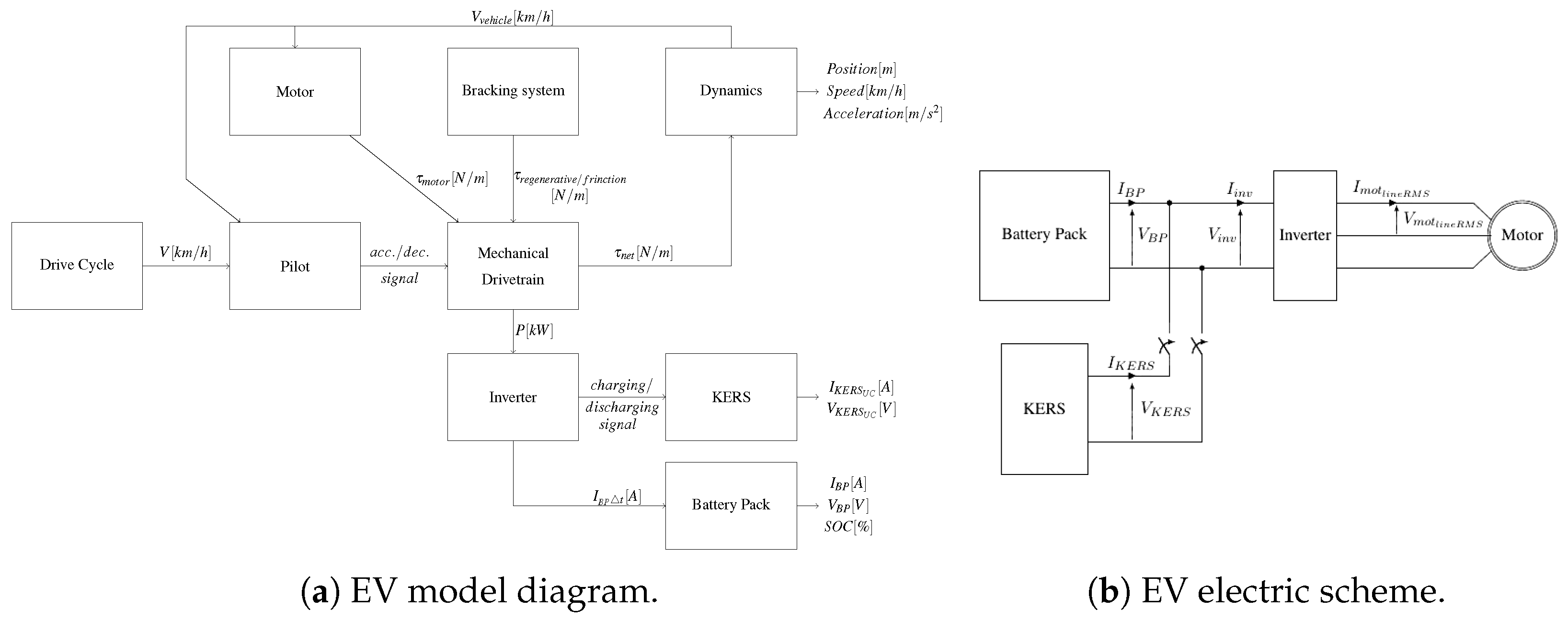
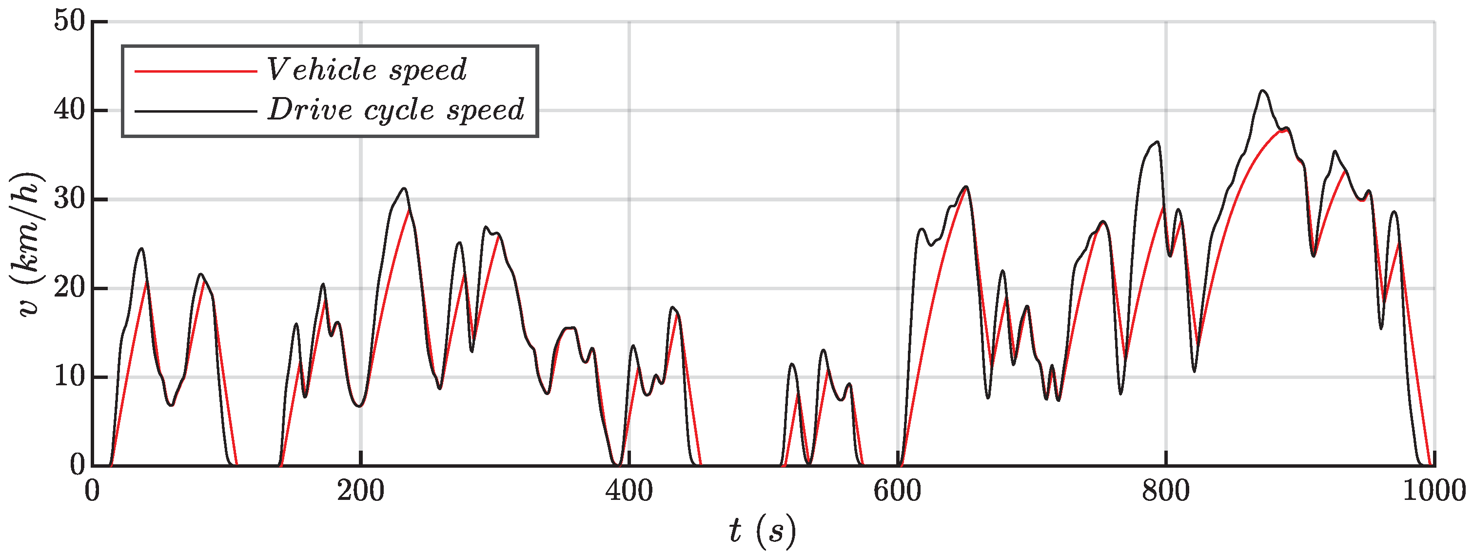
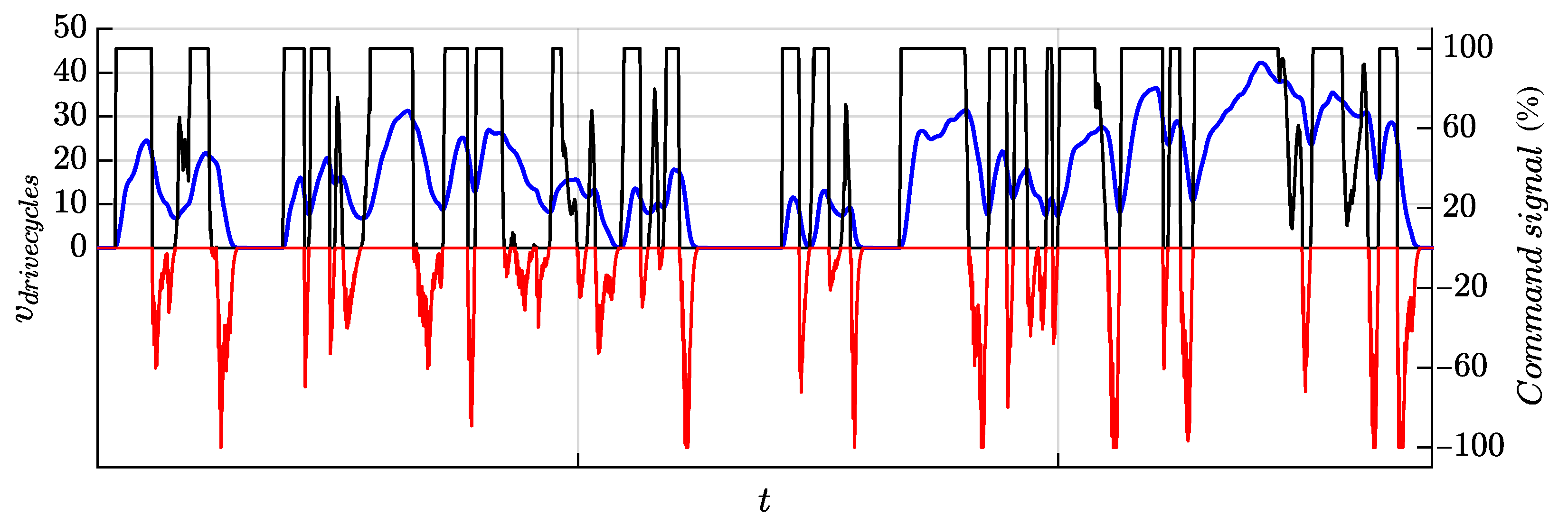
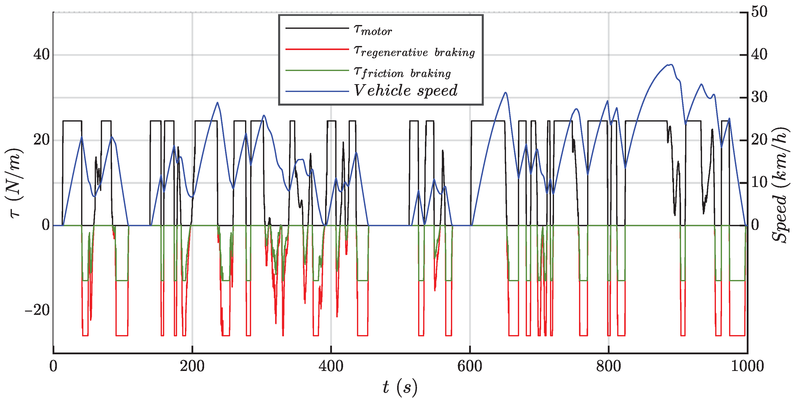
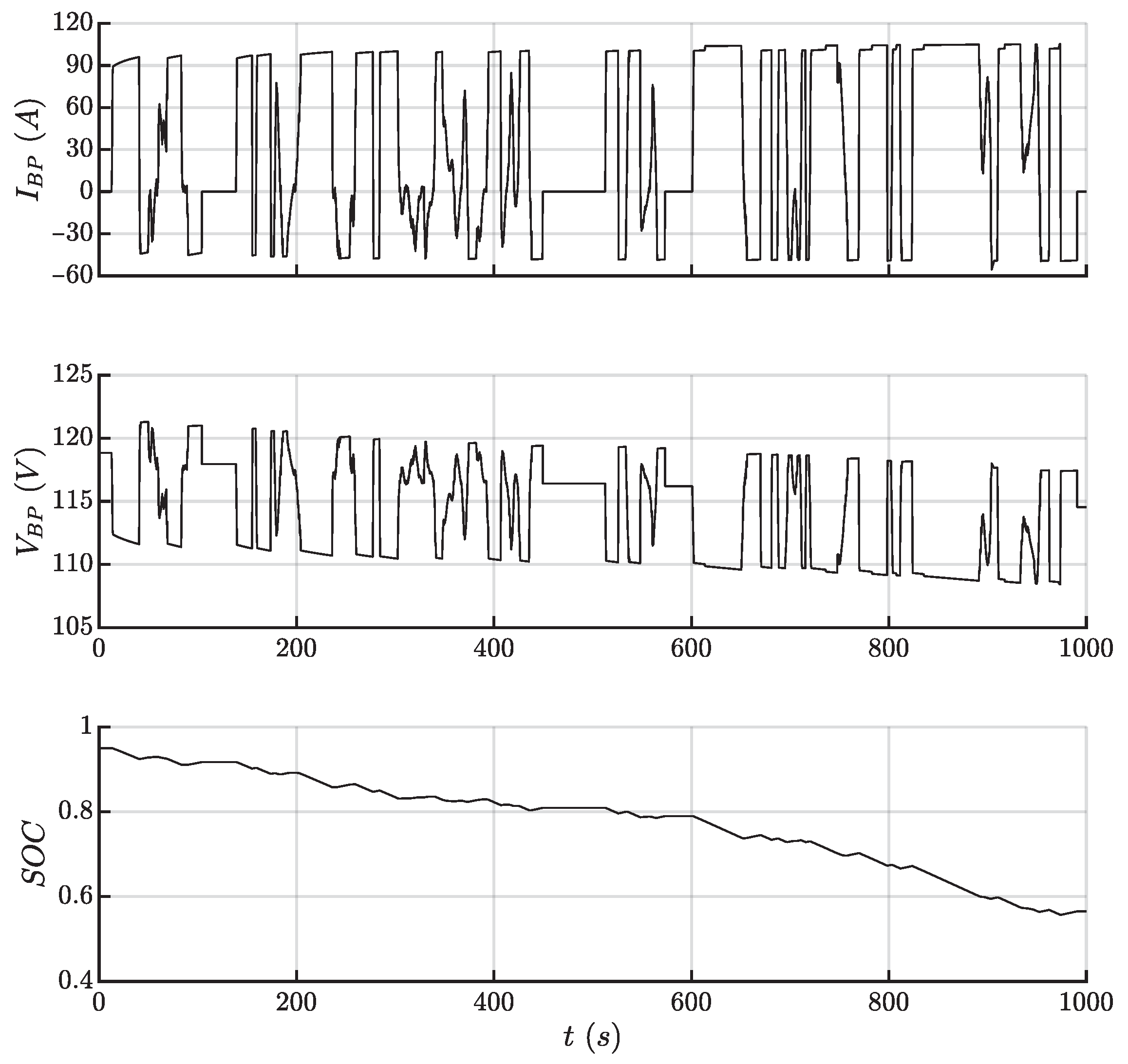
2. Formula SAE Electric Single-Seater Electric Racing Car Model
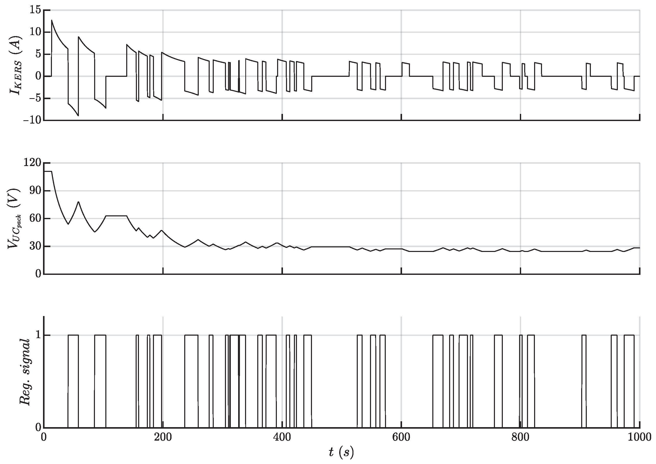
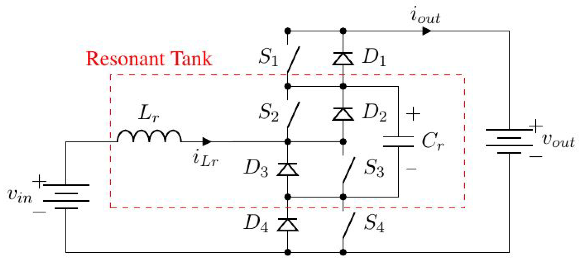
The main target of the electric racing car model is to compute, at any time step ( Δ t ) of the simulation, all the electric quantities (power, voltage, and current) at the KERS terminals.
Figure 1a shows the block diagram of the complete EV model, where one block for each sub-system of the vehicle is considered, as described in the following. Figure 1b shows the electrical diagram [12] of the EV, where the main elements and the corresponding voltages and currents are represented.
From a given speed profile, the Pilot block generates the acceleration and deceleration signals that control the motor and the braking systems, respectively. The Mechanical Drivetrain block calculates the net torque applied to the vehicle, which is the input of the Dynamics block, where the equations of motion are implemented and the driving variables such as acceleration (a), speed (v), and position (x) are computed. When braking is needed to slow down the EV, the Braking System block calculates the available regenerative energy. The model is implemented using power equations to relate the subsystems and regulate the driving simulation [5]. In the following, a detailed description of each block is provided.
Drive Cycleblock
The Drive Cycle block is the source of the reference motion data. Its outputs may be the displacement, the speed, or the acceleration. In this work, as well as in many automotive applications, the reference speed profile is considered, as shown in Figure 2.
Pilotblock
The Pilot block receives as input the target speed, from the Drive Cycle block, and the actual vehicle speed, from the Mechanical Drivetrain block. A PID controller compares these speeds and generates an acceleration or braking signal. Figure 3 shows the action generated by the Pilot block.
Motorblock
Starting from the vehicle speed, the Motor block provides the torque τ m o t generated by the motor according to its torque–speed curve.
Brakingblock
Starting from the braking signal, the Braking block compares it with the maximum regenerative torque ( τ r e g m a x ) and splits the braking torque into the allowed regenerative braking torque ( τ r e g ) and the additional friction braking torque ( τ f r i c t i o n ) that is required to properly slow down the vehicle.
Mechanical drivetrainblock Starting from the control signals and the torques generated for the direct (motor traction) or reverse operations (braking), the Mechanical Drivetrain passes to the Dynamics block the torque ( τ n e t ) applied to the vehicle: this is calculated as the algebraic sum of motor torque ( τ m o t ), the braking torque due to friction ( τ f r i c t i o n ), and the braking torque due to regenerative braking ( τ r e g e n e r a t i v e ):
τ n e t = τ m o t τ f r i c t i o n τ r e g e n e r a t i v e
During direct operations, the motor torque is greater than zero, while the braking torque due to friction and regenerative braking are both zero. On the contrary, during braking operations, the motor torque is zero and the braking torques due to friction and regenerative braking are non-negative, their values depending on the share between friction and regenerative braking. Figure 4 shows the different components of the torque at the vehicle shaft for motor traction and braking operations.
Dynamicsblock
The Dynamics block models the vehicle dynamics by means of the power balance equation. The angular acceleration ( ω ˙ m ), the angular speed ( ω m ), as well as the linear acceleration (a), the linear speed (v), and the position (x) are computed in each time step [5]. This analysis is theoretically based and implemented in 2D. The power balance of the EV is:
P m o t o r + P r e s i s t a n t + P l o s s e s = 0
where the three contributions are defined as follows.
P m o t o r is given by the electromagnetic power generated by the motor minus the power due to the motor inertia:
P m o t o r = τ m · ω m J m · ω ˙ m · ω m
where τ m is the electromagnetic torque generated by the motor, ω m is the motor angular speed, ω ˙ m is the motor angular acceleration, and J m is the motor moment of inertia.
P r e s i s t a n t is the power related to the motion resistances, which are the gravity force on a graded road, friction, aerodynamic force, and inertia:
P r e s i s t a n t = M · g · sin ( α ) · v τ r e s · ω w 1 2 · ρ a i r · S f r o n t a l · C D · v 3 J r * ω ˙ m · ω m
where M is the overall weight of both the vehicle and pilot, g is the gravity acceleration, α is the road tilt angle, τ r e s is the friction torque, ρ a i r is the density of the air, S f r o n t a l is the frontal surface of the vehicle, C D is the aerodynamic drag coefficient, v is the vehicle speed, and J r * is the equivalent vehicle rotational inertia, including the vehicle’s and wheels’ moment of inertia.
P l o s s e s represents the overall losses, assuming them linear with the electromechanical power:
P l o s s e s = ( 1 η ) · τ m · ω m
where the efficiency ( η ) takes into account the overall mechanical losses.
Concerning the inertial terms, they can be easily obtained as the first order derivative of the kinetics energy. For the motor side, it is:
d E k m o t o r d t = d d t 1 2 · J m · ω m 2 = J m · ω ˙ m · ω m
For the vehicle side, the kinetic energy terms due to both vehicle speed and wheels angular speed have to be taken into account:
d E k v e h i c l e d t = d d t 4 · 1 2 · J w · ω w 2 + 1 2 · M · v 2 = J r * · K t r 2 · ω ˙ m · ω m
where ω w is the wheels’ angular speed, J w is the wheels’ moment of inertia, R w is the wheel radius, and K t r is the transmission ratio; as a consequence, v = ω w · R w = K t r · ω m · R w . In this work, K t r is introduced for the sake of completeness; for an EV, it is usually equal to one.
The resistant torque τ r e s in (4) can be better represented by substituting the following relations:
τ r e s = M · g · cos ( α ) · f d · R w
where M · g · cos ( α ) is the net ground reaction force and f d is the dynamic friction.
By substituting (8) in (4) and substituting (3)–(5) in (2), the equation of motion becomes:
η · ( τ m J m · ω ˙ m ) · ω m = M · g · [ f d · cos ( α ) + s e n ( α ) ] · R w · K t r · ω m + + 1 2 · ρ a i r · S f r o n t a l · C D · ω m 3 · R w 3 · K t r 3 + J r * · ω ˙ m · ω m · K t r 2
Here, the net power at the motor side minus the motor inertia is equal to the sum of the rolling and grading resistances, the aerodynamic drag, and the vehicle inertia.
The angular acceleration, as well as the linear speed and the position are derived from the solution of (9).
Inverter and Storage Managementblock
Starting from the absolute value of the electromechanical power required for motion, the Inverter and Storage Management block calculates the absolute value of the power and current at the inverter DC side ( P i n v ), as follows:
P i n v = η m d · P m o t o r braking   operation P m o t o r η m d motor   traction I i n v D C = P i n v V i n v
where η m d is the overall efficiency of the motor drive, P m o t o r is the absolute value of the electromechanical power generated by the motor, and V i n v is the voltage of the vehicle DC bus, which is the same voltage applied both to the battery pack terminals ( V B P ) and to the DC bus side KERS converter terminals ( V K E R S ) . Depending on direct or reverse operation, a control signal is generated to control the KERS and to split the inverter current into the battery pack current ( I B P ) and the KERS current ( I K E R S ) .
Battery Packblock
Starting from the battery pack (BP) current ( I B P ) as input, Battery Pack block calculates the State of Charge ( S O C ) and the corresponding voltage ( V B P ) per each time step ( Δ t ) . The minimum levels of S O C and V B P work as a backstop function, and they set the operational limit to guarantee the reliability and durability of the batteries.
The battery pack model is based on the Butler–Volmer physical approach [15]. The equation that describes how the electrical current (i) through an electrode depends on the voltage difference between the electrode and the bulk electrolyte is:
i = n s F k o a o v o e β o F ( E + η ) R T k r a r v r e β r F ( E + η ) R T
where the subscripts o and r indicate the state for oxidation and reaction, respectively, n s is the number of the electrochemical steps excluding repetitions, k o and k r are the chemical equilibrium coefficients, a o v o and a r v r are the activity coefficients, F is the Faraday constant, η is the overpotential, and E is the equilibrium electrode potential. The overall cell voltage V c e l l is:
V c e l l = E + + η + E η η e l
The BP works as the main storage source of the vehicle. The battery pack layout is derived from the voltage ( V i n v ) and from the current ( I i n v ) requirements at the inverter DC side.
The number of cells in series ( n s ) and the number of strings in parallel ( n p ) are defined as:
n s = V i n v V c e l l ; n p = I i n v I c e l l N O M
where V c e l l is the rated no-load voltage of each cell and I N O M c e l l is the rated cell current. Figure 5 shows the input of the B a t t e r y P a c k block, that is the current at the BP terminals ( I B P ), and the outputs, which are the voltage at the BP terminals ( V B P ) and its State of Charge ( S O C ), along the whole drive cycle.
KERSblock
The K E R S block receives as input the logic signal from the inverter and storage management block, which is a request to activate, and calculates the KERS current ( I K E R S ) , which depends on the state of charge of the UC pack ( S O C U C ) and the allowable charge and discharge current ( I U C ) . Figure 6 shows the input of the K E R S block, which is the regulation signal, and the outputs, which are the current ( I K E R S ) and the voltage ( V U C p a c k ) at the UC terminals, along the whole drive cycle. The UC pack is sized as the BP.
The aim of this additional system is to exploit the UC peculiarities of high current capability, thermal stability, long ELD (Estimated Life Duration), and very fast behavior in both charge and discharge, to help the BP in the most critical driving phases. As shown in the first graph in Figure 6, the current capability decreases proportionally to the voltage drop during discharge. In the second graph, the voltage behavior of the UC pack is represented. The discharge voltage is limited by V U C p a c k M I N . When the voltage of the UC pack reaches the minimum value, the KERS stops operating. In the last graph, the signal that controls the regeneration during braking is displayed, where 1 means ON, while 0 is OFF.

3. KERS Converter

Resonant converters are suitable for KERS applications [12,13] due to their features of high efficiency at high switching frequency, their compactness, and their scalability. The small size of the passive components and high power density can be achieved by increasing the switching frequency. In contrast to conventional PWM converters that are based on hard switching and suffer from high switching losses [16], resonant converters use a resonant tank—an L C circuit—to turn on and turn off at zero current ( Z C S ) or zero voltage ( Z V S ) [17], resulting in negligible switching losses [18], hence high efficiency and small heat sinks [19]. The converter proposed in this work is a bidirectional Z C S converter presented by Figure 7. The bidirectional capability is obtained by adding switches S 1 and S 2 and diodes D 3 and D 4 to the original boost converter presented in [13]. This improved topology can also operate as a buck converter transferring energy from V o u t to V i n .

3.1. Topology Analysis

The operation principle, both in boost mode and in buck mode, as well as the characteristics of the chosen converter for the EV application as the KERS interface are presented here. The converter analysis is based on the following assumptions [20,21]:
  • the converter is analyzed in the steady state;
  • the switches and the diodes are treated as being ideal;
  • losses in the inductive and capacitive elements of the resonant tank are neglected;
  • the voltages at the input and output terminals are assumed to be constant.

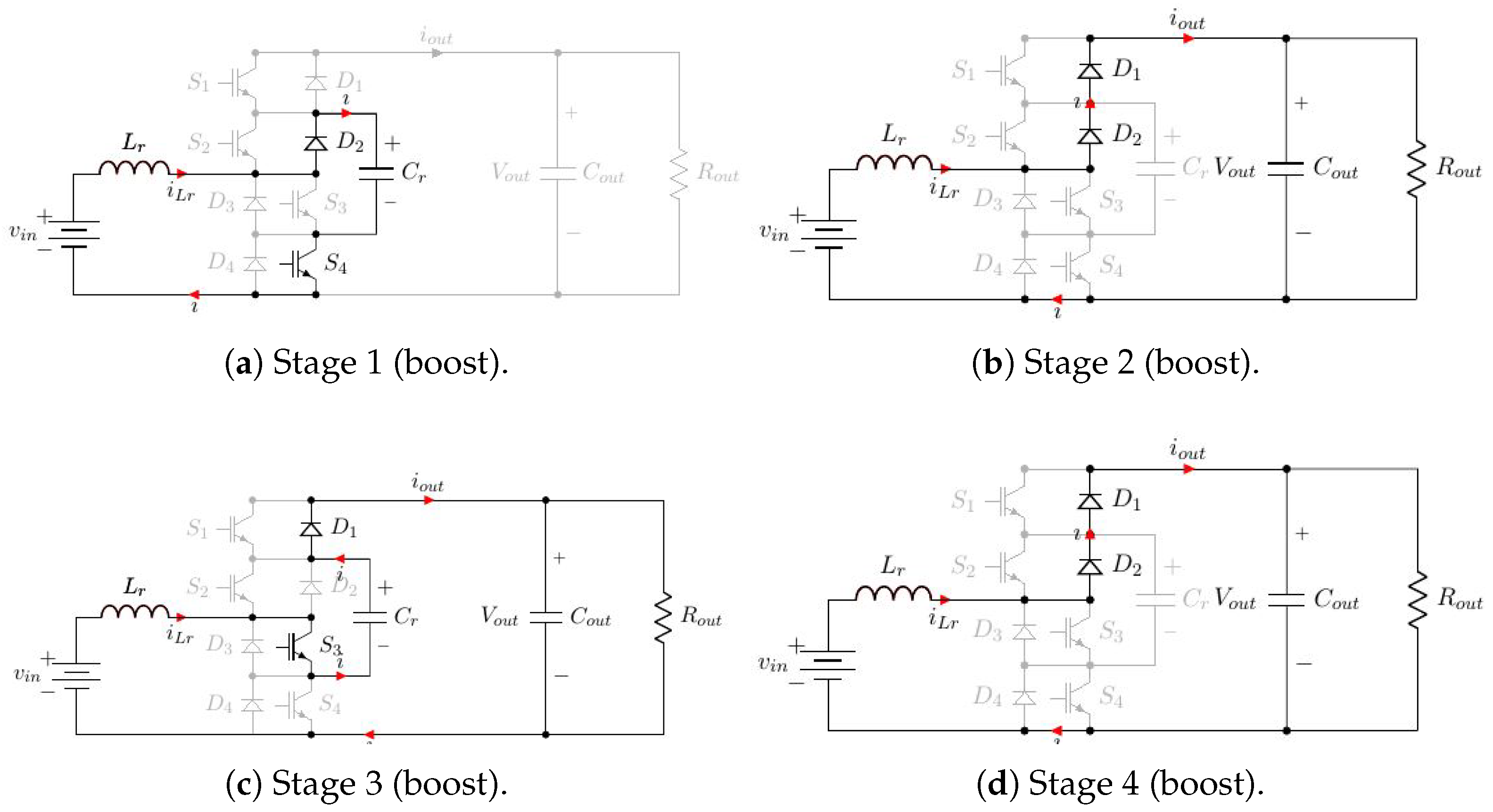
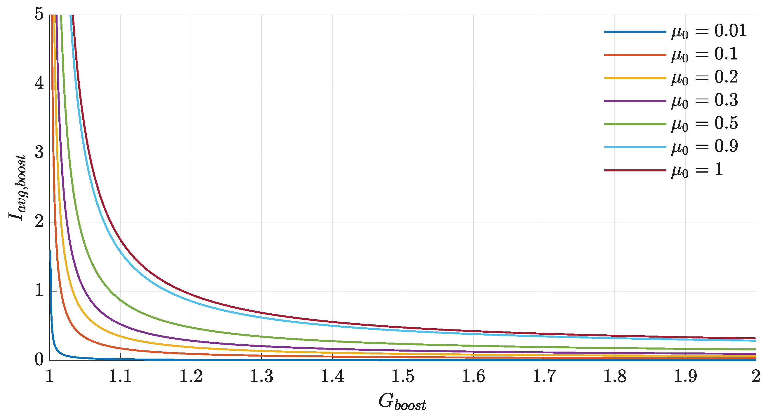
3.1.1. Boost Analysis

In boost operation mode, the pair of switches S 3 and S 4 is controlled by a complementary square-wave with a 50 % duty cycle D i , and the pair of switches S 1 and S 2 is kept in the off state. Each half switching cycle consists of three stages, as illustrated in Figure 8.
Stage 1 [ t 0 , t 1 ]
At the beginning of the switching period at t 0 :
  • the resonant tank capacitor C r and the resonant tank inductor L r are uncharged;
  • S 3 turns off, and S 4 turns on;
  • D 2 results in forward bias, and D 1 results in reverse bias.
When S 4 turns on, the resonant tank charges C r through the inductor L r . At t 1 , the voltage across C r reaches the output voltage level V o u t , D 1 becomes forward biased, and this transient ends. The inductor current is I 1 , b o o s t . The state-space equations of this stage are:
V i n = L r d i L r d t + v C r ( t ) i L r ( t ) = C r d v C r ( t ) d t
The solution of (14) in the Laplace domain [10] is:
I L r ( s ) = C r s 2 L r C r + 1 V i n V C r ( s ) = V i n / s 1 + s 2 L r C r
The inverse Laplace transformation [10] gives:
i L r ( t ) = sin ( ω 0 t ) ω 0 V i n L r v C r ( t ) = V i n [ 1 cos ( ω 0 t ) ]
where ω 0 = 1 L r C r is the resonant angular frequency.
In order to get generic results, the per unit state variables, i L r ( t ) ¯ and v C r ( t ) ¯ , are introduced:
i L r ( t ) ¯ = i L r ( t ) V i n / Z r v C r ( t ) ¯ = v C r ( t ) V i n
where Z r = L r C r is the resonant impedance. Finally, the per unit state variables are included in the state vector z:
z = v C r ( t ) ¯ + j i L r ( t ) ¯
Stage 1 is described by the following state vector:
z 1 , b o o s t = ( 1 cos ( ω 0 t ) ) + j ( sin ( ω 0 t ) )
Assuming the boost mode voltage gain defined as G b o o s t = V o u t V i n , the capacitor voltage at the end of Stage 1 is G b o o s t . Therefore, the duration of the first stage is:
Δ t 10 = t 1 t 0 = 1 ω 0 ( π arccos ( G b o o s t 1 ) )
The resulting per unit inductor current is:
i L r ( t 1 ) ¯ = I 1 , b o o s t ¯ = I 1 , b o o s t V i n / Z r = sin ( ω 0 Δ t 10 )
Stage 2 [ t 1 , t 2 ]
At the beginning of Stage 2 at t 1 :
  • v C r ( t 1 ) is equal to V o u t , and i L r ( t 1 ) is equal to I 1 , b o o s t ;
  • S 3 is still off, and S 4 is still on;
  • D 2 is still forward biased, and D 1 results in forward bias.
v C r ( t ) is equal to V o u t , and i L r ( t ) drops linearly to zero. As soon as the current in the inductor reaches zero, diode D 2 becomes reverse biased ( V o u t > V i n ) and Stage 2 ends. The state vector during Stage 2 is:
z 2 , b o o s t = ( G b o o s t ) + j ( ω 0 ( 1 G b o o s t ) + I 1 , b o o s t ¯ )
The duration of this stage can be calculated as:
Δ t 21 = t 2 t 1 = 1 ω 0 I 1 , b o o s t ¯ G b o o s t 1
Stage 3 [ t 2 , t 3 ]
At the beginning of Stage 3 at t 2 :
  • i L r ( t ) has just reached zero, and v C r ( t ) is clamped at V o u t ;
  • S 3 is still off, and S 4 is still on;
  • D 2 results in reverse bias, and D 1 is still forward biased.
i L r ( t ) = 0 , and there is no power transfer at the converter input terminals. The state vector during Stage 3 is z 3 , b o o s t = G b o o s t . It ends at half of the whole switching cycle: ω s t = π . Therefore:
ω s Δ t 32 = π ω s Δ t 21 ω s Δ t 10
Stage 4 [ t 3 , t 4 ]
At the beginning of Stage 4 at t 3 , that is the beginning of the second half of the switching period:
  • v C r ( t 1 ) is equal to V o u t , and i L r ( t 1 ) is equal to zero;
  • S 3 turns on, and S 4 turns off;
  • D 1 results in forward bias, and D 2 results in reverse bias.
Stage 4 is similar to Stage 1. The turning on of S 3 triggers the transient of the resonant tank that discharges C r . At t 4 , v C r drops to zero, D 2 becomes forward biased, and the transient ends. The Laplace transform of the state space equations during Stage 4 is:
I L r ( s ) = C r s 2 L r C r + 1 V i n V C r ( s ) = V o u t s V i n / s 1 + s 2 L r C r
The state vector during Stage 4 is:
z 4 , b o o s t = ( G b o o s t 1 + cos ( ω 0 t ) ) j ( sin ( ω 0 t ) )
The duration of Stage 4 is the same as Stage 1 ( Δ t 43 = Δ t 10 ), and the inductor current at the end of Stage 4 is I 4 , b o o s t = I 1 , b o o s t .
Stage 5 [ t 4 , t 5 ]
At the beginning of Stage 5 at t 4 :
  • v C r ( t 1 ) is equal to zero, and i L r ( t 1 ) is equal to I 4 , b o o s t ;
  • S 4 is still off, and S 3 is still on;
  • D 2 is still forward biased, and D 1 results in forward bias.
Stage 5 is similar to Stage 2. The current I L r reduce linearly to zero; the initial current is the same as Stage 2, as well as the voltage applied to L r . The state vector during Stage 5 is:
z 5 , b o o s t = 0 + j ( ω 0 ( 1 G b o o s t ) + I 1 , b o o s t ¯ )
The duration of Stage 5 is the same as Stage 2 ( Δ t 54 = Δ t 21 ).
Stage 6 [ t 5 , t 6 ]
At the beginning of Stage 6 at t 5 :
  • i L r ( t ) has just reached zero, and v C r ( t ) is zero;
  • S 4 is still off, and S 3 is still on;
  • D 1 results in reverse bias.
Stage 6 is similar to Stage 3. There is no power transfer at the converter input terminals. The state vector is z 6 , b o o s t = 0 . The duration of Stage 6 is the same as Stage 3 ( Δ t 65 = Δ t 32 ), and the end of Stage 6 corresponds to the end of the switching cycle.

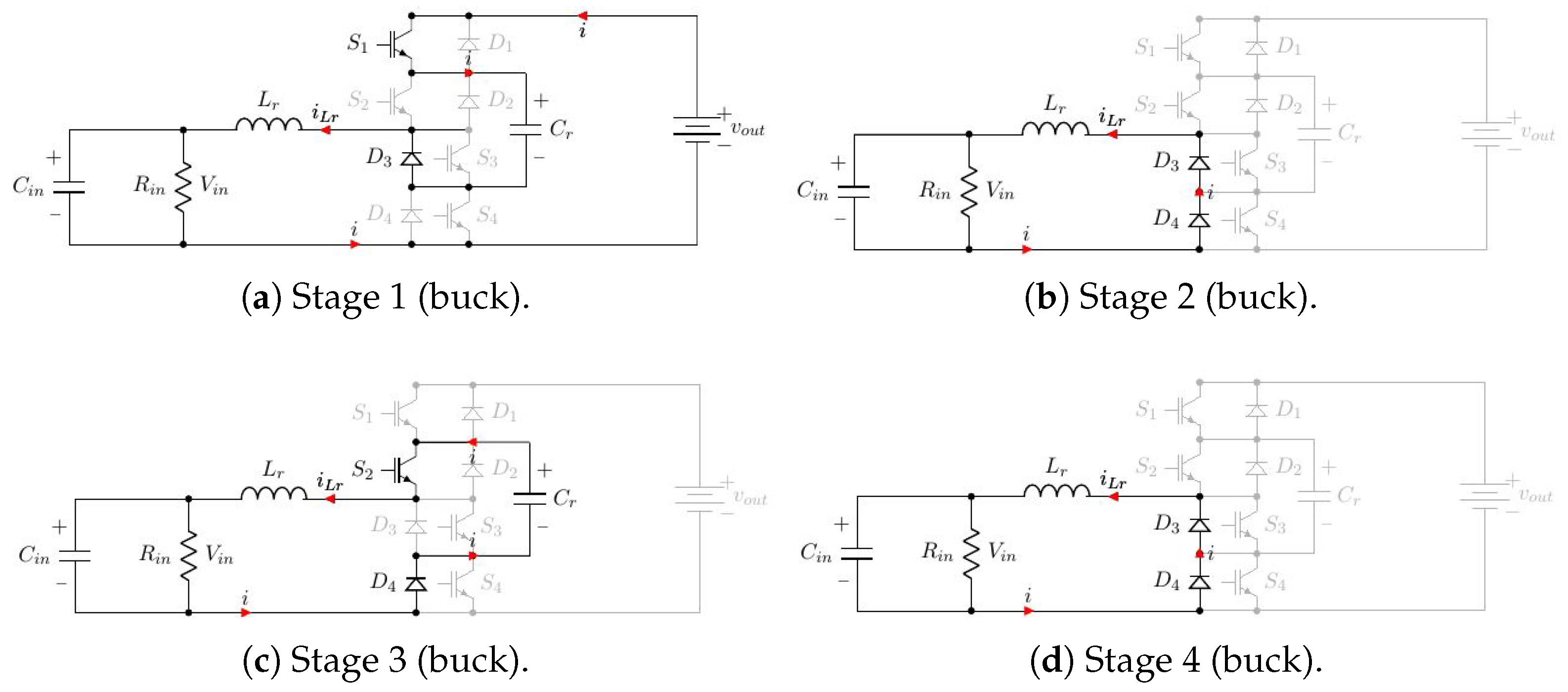
3.1.2. Buck Analysis

In buck operation mode, the pair of switches S 1 and S 2 is controlled by a complementary square-wave with a 50 % duty cycle D i , and the pair of switches S 3 and S 4 is kept in the off state. Like in boost operation mode, each half switching cycle consists of three stages, as illustrated in Figure 9. Each stage is similar to the corresponding stage in boost operation mode, and it is modeled in the same way.
Stage 1 [ t 0 , t 1 ]
At the beginning of the switching period, t 0 :
  • v C r ( t 1 ) is equal to zero, and i L r ( t 1 ) is equal to zero;
  • S 2 turns off, and S 1 turns on;
  • D 3 results in forward bias, and D 4 results in reverse bias.
The turning on of S 1 triggers the transient of the resonant tank that charges C r , which ends at t 1 , when v C r ( t 1 ) = V o u t , and D 4 becomes forward biased. The state vector and the duration of Stage 1 are:
z 1 , b u c k = ( ( 1 G b u c k 1 ) ( 1 cos ( ω 0 t ) ) ) + j ( ( 1 G b u c k 1 ) sin ( ω 0 t ) ) t 10 = t 1 t 0 = 1 ω 0 ( π arccos ( G b u c k G b u c k 1 ) )
where G b u c k = V i n V o u t . The inductor current at the end of Stage 1 is:
I 1 , b u c k = ( G b u c k 1 ) sin ( ω 0 Δ t 10 )
Stage 2 [ t 1 , t 2 ]
At the beginning of Stage 2, t 1 :
  • v C r ( t 1 ) is equal to V o u t , and i L r ( t 1 ) is equal to I 1 , b u c k ;
  • S 2 is still off, and S 1 is still on;
  • D 3 is still forward biased, and D 4 results in forward bias.
During Stage 2, v C r ( t ) is clamped at V o u t and i L r ( t ) drops linearly to zero. As soon as the current in the inductor reaches zero, diode D 3 becomes reverse biased ( V o u t > V i n ) and Stage 2 ends. The state vector and the duration of Stage 2 are:
z 2 , b u c k = ( 1 G b u c k ) + j ( I 1 , b u c k ¯ ω 0 ( t t 1 ) ) Δ t 21 = t 2 t 1 = I 1 , b u c k ¯ ω 0
Stage 3 [ t 2 , t 3 ]
At the beginning of Stage 3, t 2 :
  • i L r ( t ) has just reached zero, and v C r ( t ) is clamped at V o u t ;
  • S 3 is still off, and S 4 is still on;
  • D 3 results in reverse bias, and D 4 is still forward biased.
The state vector during Stage 3 is z 3 , b u c k = 1 G b u c k . Stage 3 ends at half of the whole switching cycle, which means ω s t = π . Therefore:
ω s Δ t 32 = π ω s Δ t 21 ω s Δ t 10
Stage 4 [ t 3 , t 4 ]
At the beginning of Stage 4, t 3 :
  • v C r ( t 1 ) is equal to V o u t , and i L r ( t 1 ) is equal to zero;
  • S 2 turns on, and S 1 turns off;
  • D 4 results in forward bias, and D 3 results in reverse bias.
Like Stage 1, the turning on of S 3 triggers the transient of the resonant tank that discharges C r . As soon as v C r has dropped to zero, at t 4 , D 3 becomes forward biased and this transient ends. The resulting state vector during Stage 4 is:
z 4 , b u c k = 1 G b u c k 1 + cos ( ω 0 t ) j 1 G b u c k sin ( ω 0 t )
As a result, the duration of Stage 4 is the same as Stage 1 ( Δ t 43 = Δ t 10 ) and the inductor current at the end of Stage 4 is I 4 , b u c k = I 1 , b u c k .
Stage 5 [ t 4 , t 5 ]
At the beginning of Stage 5, t 4 :
  • v C r ( t 1 ) is equal to zero, and i L r ( t 1 ) is equal to I 4 , b u c k ;
  • S 1 is still off, and S 2 is still on;
  • D 4 is still forward biased, and D 3 results in forward bias.
Stage 5 is similar to Stage 2: the current I L r reduces linearly to zero, then D 4 becomes reverse biased. The state vector of Stage 5 is:
z 5 , b u c k = 0 + j ( I 1 , b o o s t ¯ ω 0 ( t t 4 ) )
The duration of Stage 5 is the same as Stage 2 ( Δ t 54 = Δ t 21 ).
Stage 6 [ t 5 , t 6 ]
During all of Stage 6:
  • i L r ( t ) is equal to zero, and v C r ( t ) is equal to zero;
  • S 1 is still off, and S 2 is still on;
  • D 4 results in reverse bias.
The state vector during Stage 6 is z 6 , b u c k = 0 , and the duration of Stage 6 is the same as Stage 3 ( Δ t 65 = Δ t 32 ). The end of Stage 6 corresponds to the end of the switching cycle.

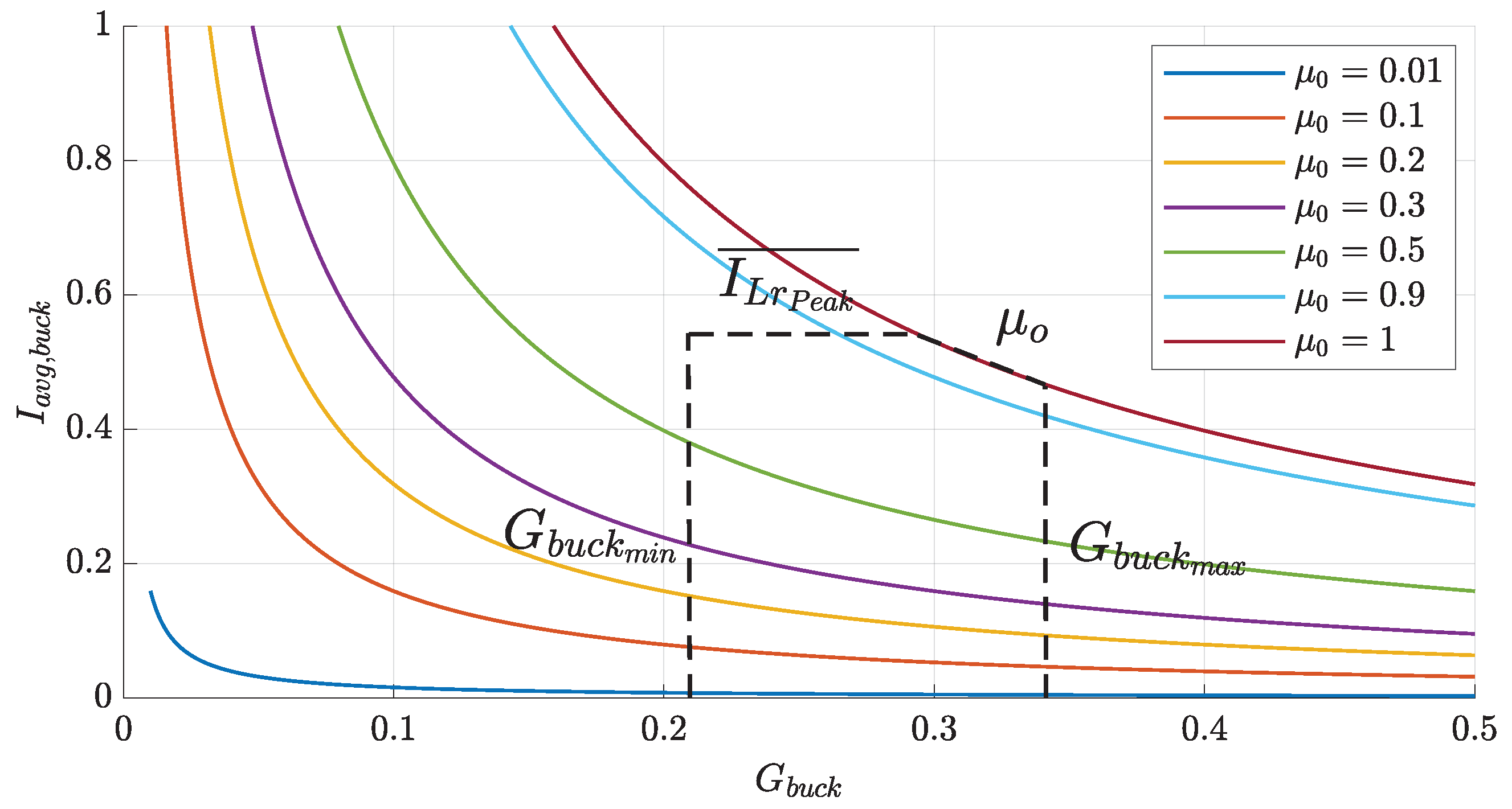
3.2. Resonant Converter Characteristics

In this section, starting from the six different stages’ analysis, the characteristics in terms of voltage gain as a function of the control strategies and the load are calculated.
In order to keep the soft switching properties, the boost gain is limited to the range 1 < G b o o s t < 2 and the switching frequency should not exceed the resonant frequency. The stable operation during Stage 2 sets the lower boundary for V o u t . The maximum voltage across the resonant capacitor at the end of Stage 1 ( 2 V i n ) sets the upper boundary for V o u t . The maximum duration of Stage 1 sets the upper boundary for the switching frequency f s , which has to be lower than or equal to the resonant frequency f 0 .
The output current in boost mode is discontinuous and is zero during Stages 1, 3, and 6. The average per unit output current i o u t A V G ¯ results in:
i o u t A V G ¯ = 1 T s [ T s i L r ( t ) ¯ d t ] = μ 0 2 π G b o o s t ( G b o o s t 1 )
where μ 0 = f s f 0 . The output power is consequently:
P o u t A V G ¯ = μ 0 2 π G b o o s t 2 ( G b o o s t 1 )
Figure 10 shows the output characteristics as a function of frequency ratio μ 0 and boost voltage gain G b o o s t . For a given frequency ratio μ 0 , the output power reduces with the increase of the boost voltage gain G b o o s t . For a given voltage gain G b o o s t , the output power increases with the frequency ratio μ 0 .
The converter operation as a function of the load depends on the output apparent resistance R o u t = V o u t I o u t A V G . In order to get generic results, the per unit output resistance is:
r o u t = R o u t Z r
The voltage gain in boost mode, as a function of the frequency ratio and per unit load, is:
G b o o s t = μ 0 2 π r o u t + 1
Since 0 < μ 0 < 1 , the converter can adjust the voltage gain in the whole range ( 1 < G b o o s t < 2 ) for loads whose per unit apparent resistance is greater than 2 π .
For the buck configuration, the average input current i i n A V G can be calculated as the sum of the integral of the current function in the topological time steps Δ t 10 , Δ t 21 , Δ t 43 , and Δ t 54 :
i i n A V G ¯ = 1 T s [ t 0 t 1 i L r ( t ) ¯ d t + t 1 t 2 i L r ( t ) ¯ d t + t 3 t 4 i L r ( t ) ¯ d t + t 4 t 5 i L r ( t ) ¯ d t ]
Solving:
i i n A V G ¯ = μ 0 2 π 1 G b u c k
The dependency of i i n A V G ¯ on the frequency ratio μ 0 and the gain G b u c k shows the same trend as the boost one.
The buck gain range is 0 < G b u c k < 0.5 .
Considering the input voltage V i n approximately constant, a constant load resistance R i n , the average input current (39), and defining r i n = R i n Z r , the gain of the buck modulation is:
G b u c k = r i n μ 0 2 π
Considering the maximum switching frequency as equal to the resonant one results in: 0 < μ 0 < 1 . Indeed, to reach the maximum gain G b u c k = 0.5 , the minimum value of r i n to be considered is 1.571 .

4. Resonant Converter Design and Simulation Results

4.1. Design Methodology

The design process of the resonant converter followed these main steps:
  • The definition of the optimal gain range for both boost and buck operations;
  • The identification, through the parameterized analysis, of the optimal value for the parameterized load r 0 ;
  • Setting the maximum allowable peak current ( I p e a k ) in the resonant inductor, switches, and diodes;
  • The choice of the switching technology for the required resonant frequency f 0 ;
  • Checking the UC pack current capability over both the charge and discharge operations.
As already discussed, in order to keep the soft switching properties, the maximum possible gain for boost operation mode is 1 < G b o o s t < 2 and for buck operation mode is 0 < G b u c k < 0.5 .
Therefore, a minimum UC pack voltage has to be set, and this limits the buck resonant operation. Therefore, the optimization process is performed based on boost mode. This means keeping as the objective: r o u t > 2 π . The resonant frequency f 0 is set based on the choice of the switches’ technology. Then, once the nominal voltage for the UC pack V U C p a c k G b o o s t , where G b o o s t = 2 , the resonant frequency f 0 = 1 2 π ω 0 , the resonant impedance Z r = L r C r , and the resonant angular frequency μ 0 are defined, the values of the resonant components are set in accordance with the equations below:
L r = Z r 2 π f 0 C r = 1 2 π Z r f 0
The switching frequency for boost operation mode is selected using (34) and (37) as:
f s b o o s t = G 1 R o u t C r
Instead, the switching frequency for buck operation mode is defined using (39) and (40):
f s b u c k = G b u c k 2 R U C p a c k C r
where R U C p a c k is the UC pack apparent resistance.
Keeping under control all the component and project constraints already mentioned, the most stringent requirement for this application is derived:
I p e a k L r > 2 π V i n v R o u t
Since V i n v should be approximately constant during operation and R o u t = V i n v 2 P i n v is very low, the minimum possible value for I p e a k L r is very high. Moreover, thus results in a peak current at the input terminals of the UC pack.
To reduce the impact of the high peak current on the resonant converter design, two solutions can be adopted:
  • Reduce the power capability of the converter; a capability factor k is defined setting the maximum gain of the converter G b o o s t = 2 and the maximum input current at the UC pack I U C p a c k = I m a x :
    k = I U C p a c k V U C p a c k G b o o s t P i n v
    Therefore, the capability of the system P K E R S is defined by P K E R S = k P i n v .
  • Use more than one converter in interleaving mode [22,23]; assuming a reasonable number of converters ( n r e s c o n v = 2 ), the power capability of each one becomes:
    P r e s c o n v = k P i n v n r e s c o n v
    This choice can halve the power capability of each converter, thus the input current, while increasing the current peak to the UC pack of just a factor of 2 . The resulting peak current in the UC pack is:
    I U C p a c k p e a k = 2 I p e a k L r
Combining these two effects, it is possible to define the whole system capability value k that makes each resonant converter respect all the constraints:
k = I U C p a c k m a x V i n v 2 n r e s c o n v e 2 π 2 V U C p a c k P i n v
Therefore, the converter can exploit the boost resonant characteristics along all the allowable gain range, and the working limits of buck operation in current, gain, and switching frequency are reported in the Figure 11. Table 1 reports the design and simulation data considered in this paper.
Outside the boost and buck resonant areas, a change in modulation strategy from resonant to a conventional PWM operation is required (hybrid modulation). However, going through the KERS analysis as designed, it appears clear that the contribution of the system to the whole current required is pretty low. Figure 12 shows that, despite the full charge of the UC pack, the KERS is not able to provide or absorb more than 15% of the total current.
The peak current in the resonant inductor ( I L r ) depends on the specific operating conditions. The reason just analyzed in (44) is appreciable from Figure 13: at G b o o s t = 2 , while I L r is greater than 70 A, the average output current is around 10 A (for each converter).
Furthermore, to avoid inductor current saturation in any working condition, it shall be designed at a higher value than the peak current. Therefore, considering the DCM behavior of the converter, the main drawback is the low average current capability compared to the weight and dimensions of the resonant inductor. Then, since during the race (as well as in the simulated speed cycle shown in Figure 2), the acceleration times are much longer and more frequent than the braking ones and since the KERS system is not able to absorb an important amount of the braking energy, the UC pack quickly runs out of charge.

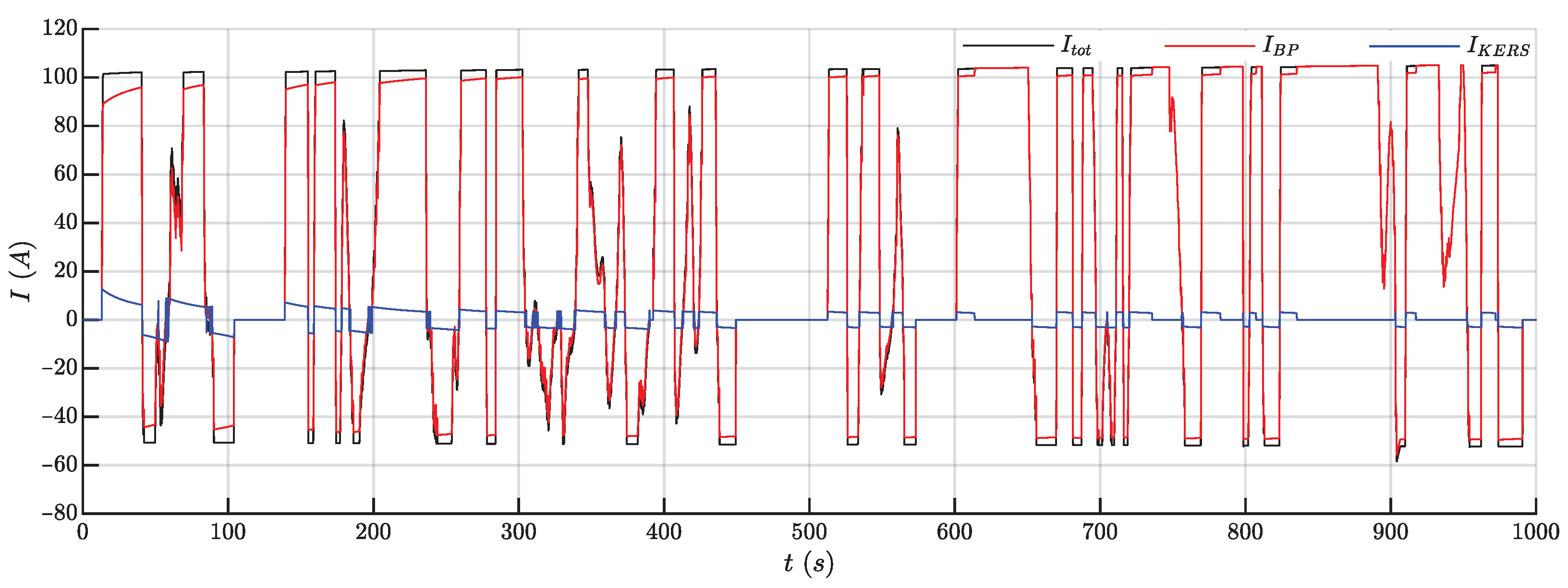
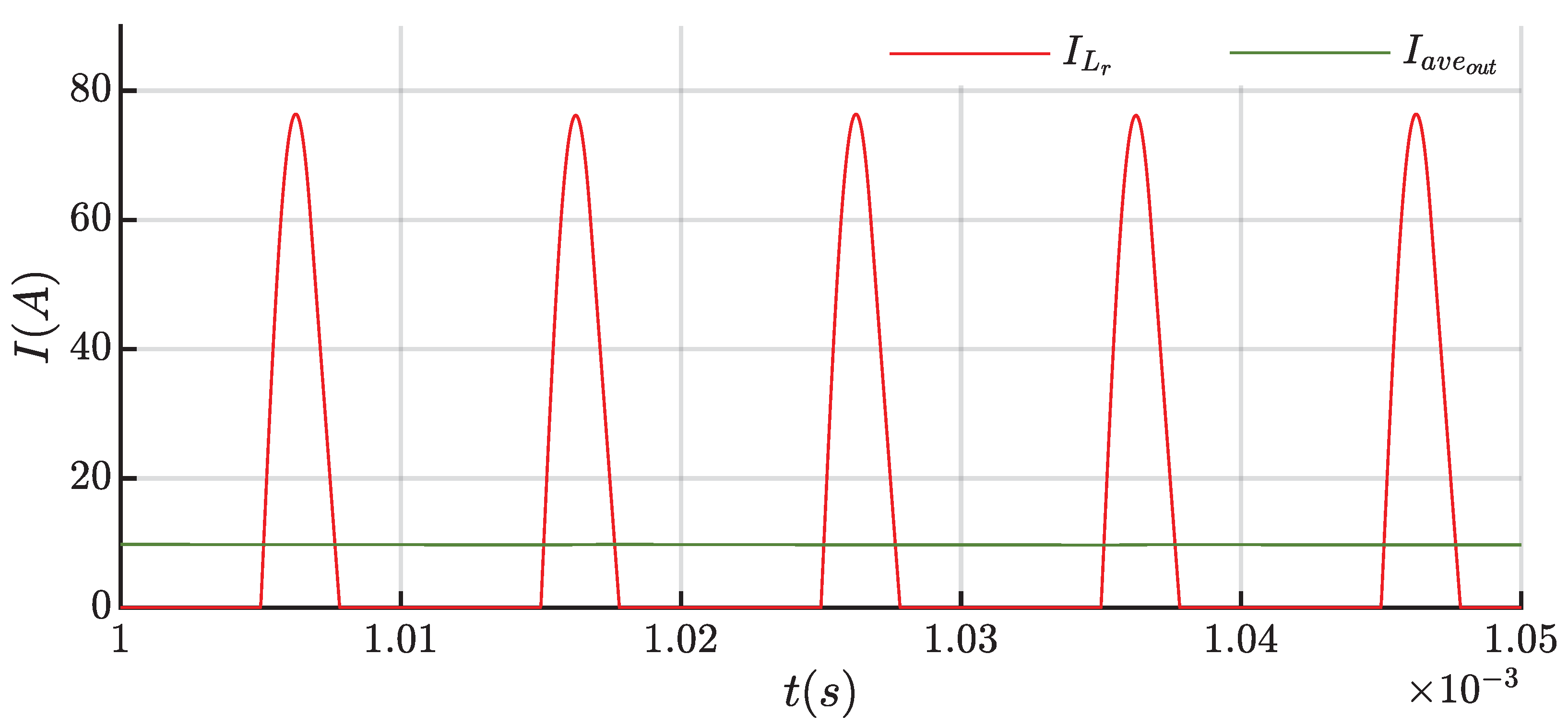
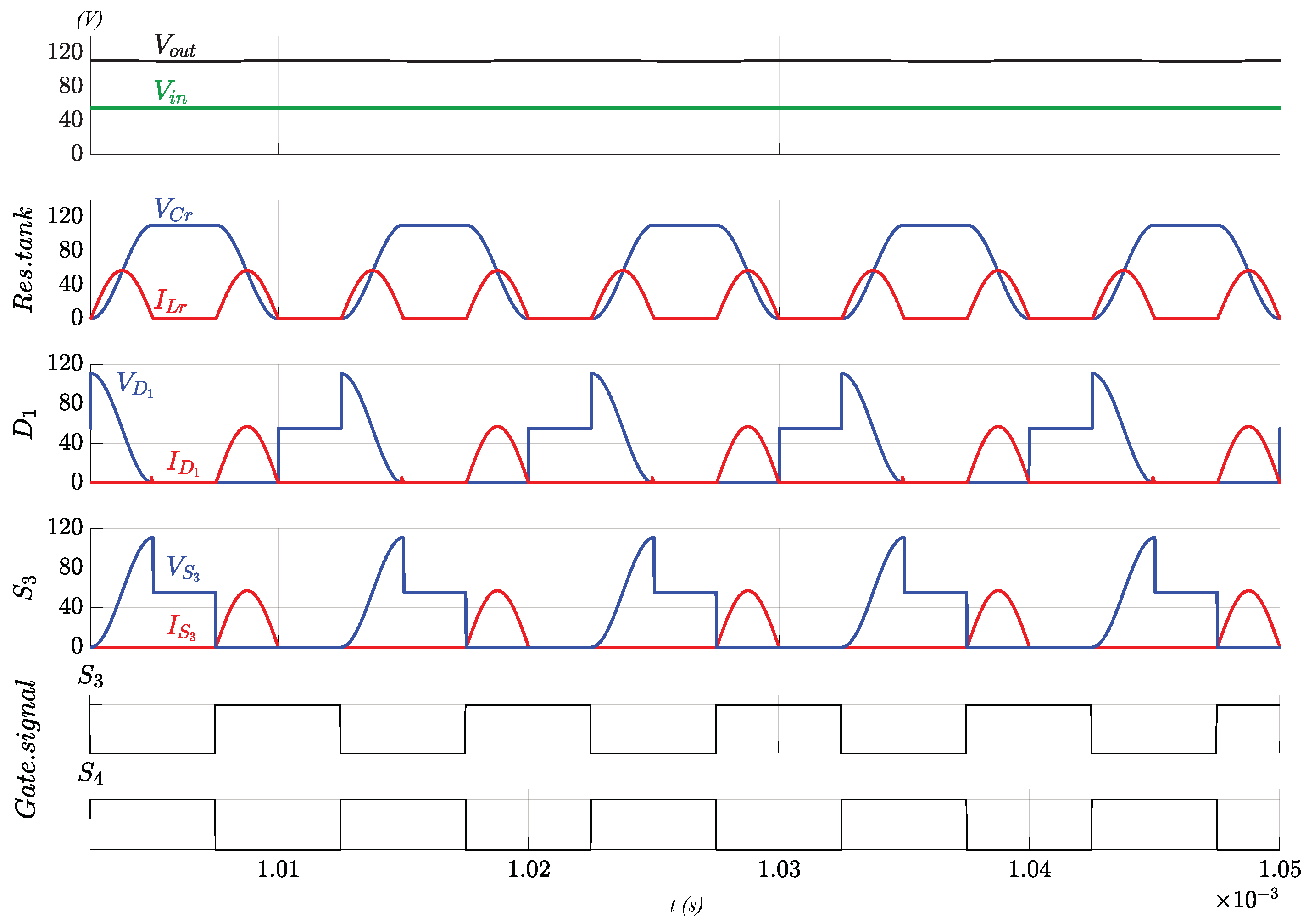
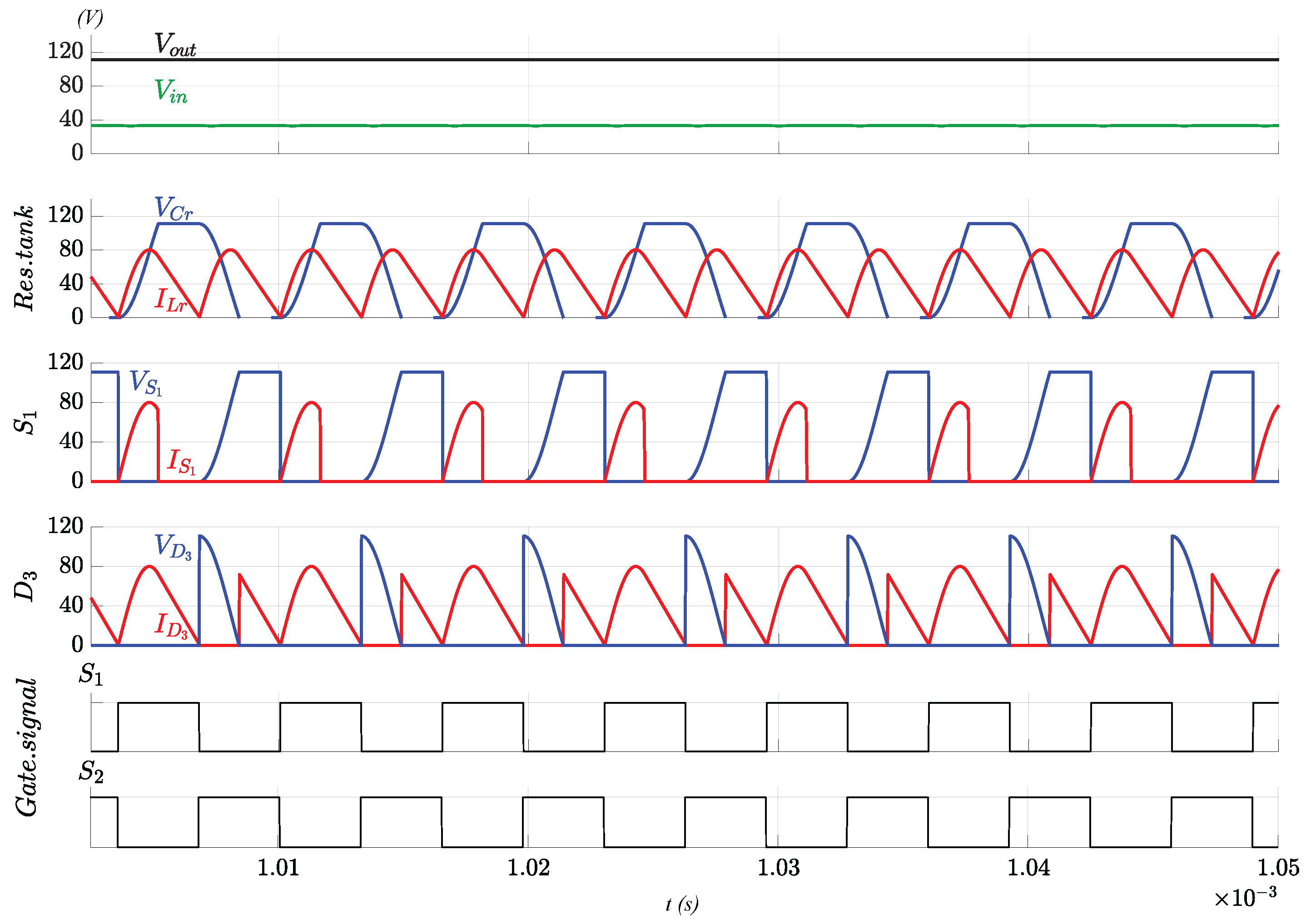
4.2. Resonant Converter Simulation Results

For boost switching mode, the main waveforms of the voltages and currents of the components are shown in Figure 14. As expected from theory, the resonant capacitor V C r is charged to V o u t and then clamped at this value during the first half switching cycle. Then, in the second half switching cycle, the resonant capacitor is discharged to zero. The frequency of the current through the resonant inductor i L r is twice the switching frequency. The average value of the current through the diodes is dependent on the switching frequency, then the output voltage can be regulated by varying the ratio between the switching frequency and the resonant frequency ( μ 0 ).
In Figure 14, the voltage and the current values of the resonant tank, one diode, and one switch are displayed. In the first one, the ability of the converter to reach V o u t and the stability of the solution at the nominal operation of G b o o s t = 2 are reported. In the second one, the current through the resonant inductor and the voltage across the resonant capacitor are shown. The third and the forth display the current and voltage behavior through respectively diode D 1 and switch S 3 . It is important to underline that there is no overlapping of voltage and current for all the switching cycle operations. This means that in this ideal simulation, the switching losses are null and that the soft switching properties of the resonant converter are kept.
Figure 15 shows the buck simulation results. In buck operation, the waveforms of the voltage and current are plotted according to the switching signal. In this operation mode also, at turn-on and turn-off, the voltage and current waveforms of the switches have no overlap and the soft switching properties of the resonant converter are kept.
The behavior of the resonant tank is exactly the same as the boost analysis.
The simulation was performed at the maximum resonant gain G b u c k = 0.3 . As expected by the theoretical limitations, the charge and discharge times of the resonant inductor are equal to the semi-period. Therefore, this confirms the limitations of the resonant operations.

5. Conclusions

The analysis performed showed that the proposed electric vehicle is able to meet the requirements of the dynamical tests of the Formula SAE Electric competition. The simulation clearly confirms the correct sizing of the storage system with a good safety margin for real operation in which the prototype could exploit the full motor power. As expected, the Li-ion cells charge and discharge according to the theoretical implementation, complying with the current and voltage operational constraints on the inverter DC side. Instead, the KERS operation is strongly influenced by the state of charge of the UC pack that is disconnected under a certain voltage value to ensure the proper operation of the whole system.
The theoretical analysis of the resonant converter shows the full capability of the resonant converter to operate under soft-switching (ZCS) properties in both buck and boost operation while keeping the simplicity and a low count of the components. The limitations due to the high current EV application pushed the analysis to correctly sizing it. An interleaved solution combined with the introduction of the capability factor achieves the result of reducing both the peak current in the resonant inductor and both the input current to the UC pack. This converter can be easily paralleled, and the switches driving signals can be shifted, reducing current ripples at the input and output capacitor, as shown for the unidirectional boost [24] version. The findings suggest that the assumptions of the compactness and low weight of the converter can be achieved and that the UC can co-work with the BP. Nonetheless, the converter is not able to fully exploit the peculiarities of the fast charge and discharge of the UC. Anyway, the ultracap technology implemented in the model remains an interesting asset to get the maximum advantage from regenerative braking.
Future works will deal with the development of a small-scale resonant converter prototype for experimental tests, as well as the study of solutions based on this converter topology, which will allow overcoming the issues related to the large peak current into the resonant tank inductor as compared to the average input current, making the converter even more suitable for an electric racing car.

Author Contributions

Conceptualization, A.D. and S.L.; methodology, A.D.; software, A.D.; validation, A.D., S.L., and G.M.; data curation, M.M.; writing, original draft preparation, A.D. and G.M.; writing, review and editing, M.M.; visualization, M.M.; supervision, S.L. and Y.R.d.N. All authors read and agreed to the published version of the manuscript.

Funding

This research received no external funding.

Data Availability Statement

Not applicable.

Conflicts of Interest

The authors declare no conflict of interest.

References

  1. World Energy Outlook 2018 (02–2019). Available online: https://www.iea.org/weo2018/ (accessed on 25 November 2020).
  2. World Bank Data about Transport Emissions (02–2019). Available online: https://data.worldbank.org/indicator/EN.CO2.TRAN.ZS (accessed on 25 November 2020).
  3. International Energy Agency Emission Statistics (02–2019). Available online: https://www.iea.org/statistics/co2emissions (accessed on 25 November 2020).
  4. Formula SAE Electric Regulations (02–2019). Available online: https://www.fsaeonline.com/cdsweb/gen/DocumentResources.aspx (accessed on 25 November 2020).
  5. Ehsani, M.; Gao, Y.; Gay, S.E.; Emadi, A. Modern Electric, Hybrid Electric, and Fuel Cell Vehicles; Chap. (2,4,6,10,11); CRC press: Boca Raton, FL, USA, 2018. [Google Scholar]
  6. Mid-Eum, C.; Jun-Sik, L.; Seung-Woo, S. Real-Time Optimization for Power Management Systems of a Battery/Supercapacitor Hybrid Energy Storage System in Electric Vehicles. IEEE Trans. Veh. Technol. 2014, 63, 3600–3611. [Google Scholar]
  7. Zhang, L.; Wang, Z.; Hu, X.; Sun, F.; Dorrell, D.G. A comparative study of equivalent circuit models of ultracapacitors for electric vehicles. J. Power Sources 2015, 274, 899–906. [Google Scholar] [CrossRef]
  8. Zou, Z.; Cao, J.; Cao, B.; Chen, W. Evaluation Strategy of Regenerative Braking Energy for Supercapacitor Vehicle; ISA Transactions; Elsevier: Amsterdam, The Netherlands, 2015; Volume 55, pp. 234–240. [Google Scholar]
  9. Radhika Kapoor, C.; Mallika, P. Comparative Study on Various KERS. In Proceedings of the World Congress on Engineering 2013 Vol III, WCE 2013, London, UK, 3–5 July 2013. [Google Scholar]
  10. Yu, S.; Chen, R.; Viswanathan, A. Survey of Resonant Converter Topologies; Reproduced from 2018 Texas Instruments Power Supply Design Seminar SEM2300© 2018; Texas Instruments Incorporated: Dallas, TX, USA, 2018. [Google Scholar]
  11. Barbi, I.; Pöttker, F. Soft Commutation Isolated DC-DC Converters; Springer: Berlin/Heidelberg, Germany, 2019. [Google Scholar]
  12. Zhang, Y.; Cheng, X.; Yin, C.; Cheng, S. A Soft-Switching Bidirectional DC-DC Converter for the Battery Super-Capacitor Hybrid Energy Storage System. IEEE Trans. Ind. Electron. 2018, 65, 7856–7865. [Google Scholar] [CrossRef]
  13. Shuai, P.; De Novaes, Y.R.; Canales, F.; Barbi, I. A Non-Insulated Resonant Boost Converter. In Proceedings of the 2010 Twenty-Fifth Annual IEEE Applied Power Electronics Conference and Exposition (APEC), Palm Springs, CA, USA, 21–25 February 2010. [Google Scholar]
  14. MATLAB and Simulink Racing Lounge: Vehicle Modeling. Available online: https://it.mathworks.com/matlabcentral/fileexchange/63823-matlab-and-simulink-racing-lounge-vehicle-modeling (accessed on 25 November 2020).
  15. Morey, T.; Pressman, A.; Billing, K. Switching Power Supply Design, 3rd ed.; McGraw-Hill: New York, NY, USA, 2009. [Google Scholar]
  16. Tabisz, W.A.; Jovanovic, M.M.; Lee, F.C. High-frequency multi-resonant converter technology and its applications. In Proceedings of the International Conference on Power Electronics and Variable Speed Drives, London, UK, 17–19 July 1990; pp. 1–8. [Google Scholar]
  17. Med, M.; Tore, M.U.; William, P.R. Power electronics: Converters, Applications and Design, 2nd ed.; Chap. (2,9); John Wiley Sons: Hoboken, NJ, USA, 1995. [Google Scholar]
  18. Hua, G.; Lee, F.C. An overview of soft-switching techniques for pwm converters. In Proceedings of the International Conference on Power Electronics and Motion Control, Beijing, China, 27–30 June 1994; pp. 801–808. [Google Scholar]
  19. Rashid, M.H. Power Electronics Handbook; Chap. 15; Academic Press: Cambridge, MA, USA, 2001. [Google Scholar]
  20. Lee, F.C. High-frequency quasi-resonant and multi-resonant converter technologies. In Proceedings of the 14 Annual Conference of Industrial Electronics Society, Singapore, 24–28 October 1988; pp. 509–521. [Google Scholar]
  21. Robert, W. Erickson, Dragan Maksimovic. In Fundamentals of Power Electronics, 2nd ed.; Springer: Boston, MA, USA, 2001. [Google Scholar]
  22. Orietti, E.; Mattavelli, P.; Spiazzi, G.; Adragna, C.; Gattavari, G. Two-phase interleaved LLC resonant converter with current-controlled inductor. In Proceedings of the Brazilian Power Electronics Conference, Bonito-Mato Grosso do Sul, Brazil, 27 September–1 October 2009. [Google Scholar]
  23. Yi, J.H.; Choi, W.; Cho, B.H. Zero-Voltage-Transition Interleaved Boost Converter With an Auxiliary Coupled Inductor. IEEE Trans. Power Electron. 2017, 32, 5917–5930. [Google Scholar] [CrossRef]
  24. Shuai, P. Investigation of a Non-insulated Resonant Converter for Power Processing of Alternative Energy Sources; Institute for Power Electronics and Electrical Drives (ISEA) RWTH-Aachen University: Aachen, Germany, 2009. [Google Scholar]
Figure 1. Overall EV model diagram and EV electric scheme. KERS, Kinetic Energy Recovery System.
Electronics 10 00161 g001
Figure 2. Vehicle speed profile vs. drive cycle speed.
Electronics 10 00161 g002
Figure 3. Input speed profile (blue), command signal (black), and acceleration/deceleration signal intensity.
Electronics 10 00161 g003
Figure 4. Net torque components.
Electronics 10 00161 g004
Figure 5. Battery pack current, battery pack voltage, and state of charge.
Electronics 10 00161 g005
Figure 6. KERS current, resulting UC voltage, and regeneration brake control signal (Reg. signal).
Electronics 10 00161 g006
Figure 7. Resonant buck-boost converter.
Electronics 10 00161 g007
Figure 8. Representation of the topological stages.
Electronics 10 00161 g008
Figure 9. Representation of the buck topological stages.
Electronics 10 00161 g009
Figure 10. Output current as a function of voltage gain; the switching frequency is a parameter.
Electronics 10 00161 g010
Figure 11. Current, gain, and switching frequency: limits in buck operations.
Electronics 10 00161 g011
Figure 12. Currents along the whole drive cycle: KERS current (blue), battery pack current (red), and total current (black).
Electronics 10 00161 g012
Figure 13. Inductor peak current and average output current.
Electronics 10 00161 g013
Figure 14. Boost simulation.
Electronics 10 00161 g014
Figure 15. Buck simulation.
Electronics 10 00161 g015
Table 1. Design and simulation data.
SymbolQuantityValueUnits
Z r Resonant impedance 0.9694 ( Ω )
L r Resonant inductor 7.71   ×   10 7 ( H )
C r Resonant capacitor 8.21   ×   10 7 ( F )
ω 0 Resonant angular frequency 0.1256   ×   10 6 ( rad / s )
kSystem capability16 (%)
P r e s . c o n v Resonant converter power capability 1.0122 ( k W )
R o u t Equivalent resonant converter output resistance 11.18 ( Ω )
r i n Parameterized input resistance 0.733 -
G b u c k Buck gain0.3 -
f s b u c k Buck switching frequency154.2 ( k Hz )
f 0 Resonant frequency200 ( k Hz )
R s n u b b e r Snubber resistance 10   ×   10 5 ( Ω )
R o n s Internal resistance 10   ×   10 5 ( Ω )
C s n u b b e r Snubber capacitance i n f ( F )
G b o o s t Nominal boost gain2 -
n r e s . c o n v Number of resonant converter2 -
r o u t Parameterized output resistance 2 π -
Publisher’s Note: MDPI stays neutral with regard to jurisdictional claims in published maps and institutional affiliations.

