1. Introduction
In high energy physics, several detectors have played a very important role in the study of particles produced by colliding ions. One of these is the gas-based electron multiplier (GEM) used for the detection of produced particles, such as [
1,
2]. Chernyshova et al. in [
3] presented an application of a GEM detector in the development of a tungsten-level monitoring system in ITER of the WEST tokamak project. A.F. Buzulotskov in [
4] presented its use in radiation systems. A complete X-ray fluorescence spectroscopy (XRF) imaging system based on a standard 10 cm × 10 cm 3-stage gas electron multiplier (GEM detector) was presented in [
5]. As well as works related to the Gas Electron Multiplier (GEM) detector soft X-ray spectroscopy system for tokamak applications used GEM detector has one-dimensional, 128-channel readout structure, reprocessing algorithms are implemented in the FPGAs in which the scope of the work is an FPGA-based implementation of the recorder of the raw signal from GEM detector [
6,
7]. FPGA and Embedded System-Based Fast Data Acquisition and Processing for GEM detectors [
8] are used for detection of ionizing radiation and Gas electron multiplier (GEM) detectors from the works [
4,
9].
In operation, small discharges are generated that can deteriorate the material of the GEMs. These discharges have been documented in the literature. A. Deisting et al. in [
10] studied the secondary discharges that occur in a GEM detector in normal operation. The authors presented a mitigation proposal by means of the use of resistors connected in series to the voltage source. Utrobicic et al. in [
11] presented the study of delayed discharges that occur in a GEM. These discharges in the detectors can damage the material, requiring the monitoring of the current consumption in GEM detectors at very short time interval order of 1ms. Deyang Yu et al. in [
12] presented the design of a picoammeter for application in measurements of charged particle beam current distribution based on the use of instrumentation amplifiers.
The design of a floating nanoammeter for the measurement of small currents in high-voltage systems and its communication system based on optical fiber was presented in [
13]. Chao et al. [
14] presented an accurate low current measurement circuit following a Faraday cup which was developed to monitor the beam current at pA range that consisted of a picoammeter with a bandwidth of 1 kHz and a gated integrator (GI). A. Utrobicic et al. in [
15] describe a floating nanoammeter used for monitoring gas detector discharge micropatterns (GEM), which consists of 16 channels, a 16-bit ADC, a lithium battery, and a 1 kHz readout. Its operating range is 0–125 nA with a resolution of 6.5 pA. An FPGA processes data from several nanoammeters which are transferred through optical fiber and sent to the PC by means of a USB 2.0 connection.
Some of the GEM applications are in ultrafast soft x-ray plasma diagnostics using small pick-up pads (pixels) in the read-out plane; the detector can achieve unambiguous two-dimensional imaging of soft X-rays at rates up to 4 MHz/pixel. This type of detector is in development for plasma diagnostics at Tokamak fusion machine [
16]. Developing a device capable of on-line control and verification of the radiation treatment of cancer patients is of critical importance. It consists of two consecutive detectors in the same gas vessel, one optimized for keV and the other for MeV photon detection. It is being developed by a group at Karolinska Institute and Royal Institute of Technology, Stockholm [
17]. The design of x-ray polarimeter for astrophysics that consist in a single GEM detector with small pads readout provides good efficiency for detection of soft X-rays, and sufficient accuracy to measure the average angle of emission of the emitted photoelectron [
18].
In the aforementioned works, in some cases, the use of batteries to generate floating ground is not pertinent, because they need to be changed some time and, depending of the application, the detector and the current monitor are not easily reachable for example in high energy physics experiments in large spectrometers. Therefore, the proposal designed in this work for high energy applied research has not been reported in the scientific literature, and in some cases, the structure they present is different from that of this study in which will be a matter of interest for researchers.
This paper presents a system to monitor the current within three levels autoscaled from 0 to 10 A with high-voltage insulation up to 5 kV collecting data at a sampling frequency of 1 kHz. The current monitor consists of three ammeters of different ranges, the first from 0 to 90 nA, the second from more than 90 nA to 900 nA, and the third from more than 900 nA to 10 A. Depending on the current, the adequate scale is automatically selected. The main contributions of this work are the following.
The use of optocouplers to transmit digital signals between the ADC and the FPGA with high-voltage insulation.
Some techniques are implemented to reduce electromagnetic interference (EMI) by using vias around ground semi-planes, capacitors connected between supply voltage (VCC) and ground to produce low impedance points for alternative current signals.
The above allows the use of a DC-DC converter powered by a conventional 10 V power supply, to generate three voltages +12 V, −12 V, and +5 V, referenced to the same floating ground, instead of using batteries.
A current monitoring system that can change scale automatically.
A new array of resistors and diodes to protect the amplifier and ADC from discharges.
A current monitor on a GEM is required to observe the deterioration of the detector, and the currents of a new GEM can range from hundreds of pA to nA and as the detector degrades its current can be of the order of microampere. The current consumption of the GEM is a function of its active area. The ammeters proposed above use batteries to reduce noise and operate in a fixed range, so the battery must be changed every so often. In this proposed design, the power of the ammeters is provided by a conventional C.D power supply, and it can also provide an automatic scale change that allows more accurate measurements at small current values. This manuscript is structured as follows. In the first part, the description of the current monitoring system is presented, continuing with the prototype of the current monitor, the experimental results, and finally the conclusions.
2. Design of the Current Monitor
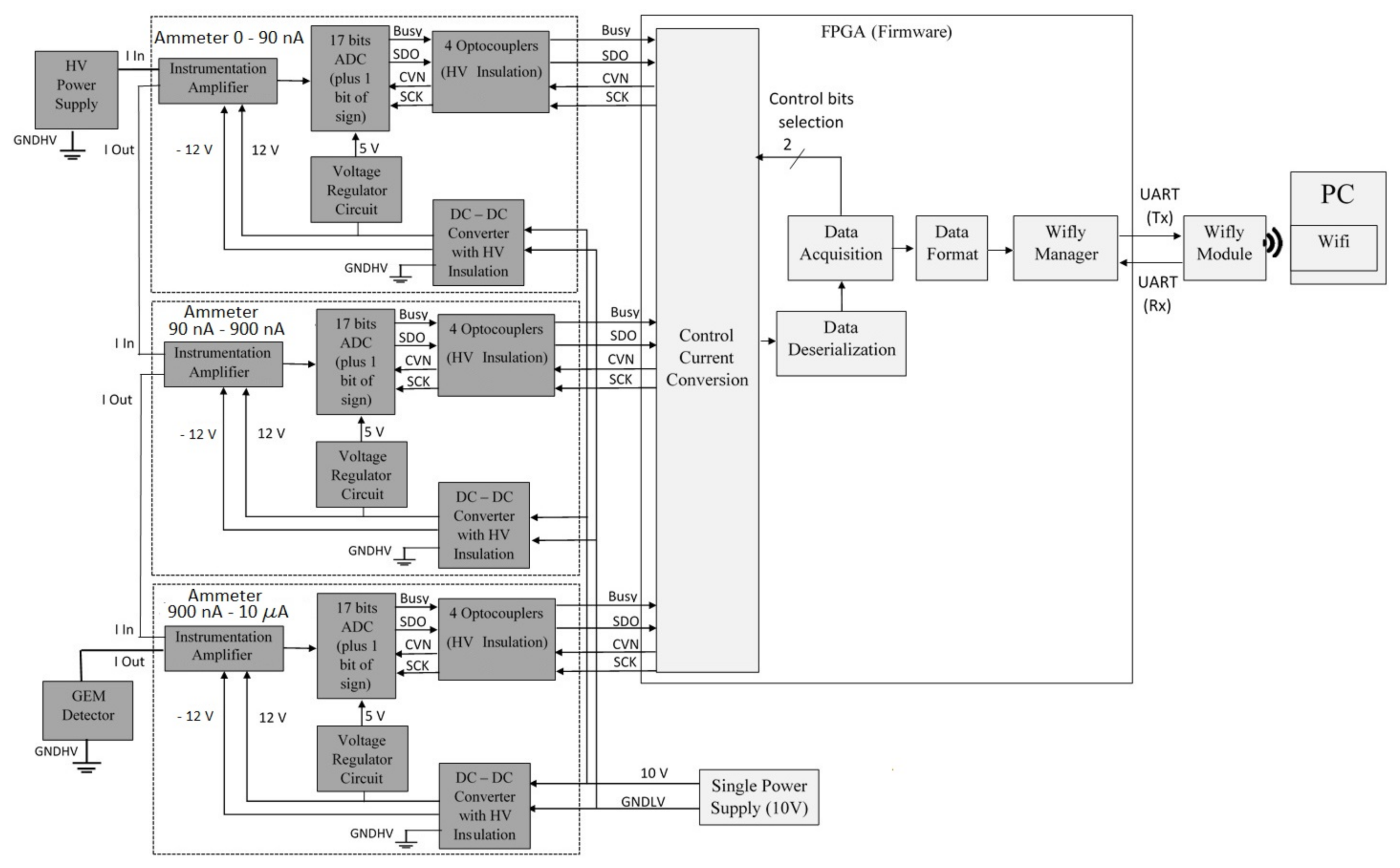
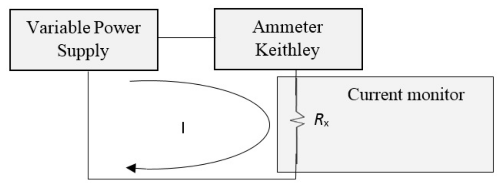
The system to monitor the current is described in
Figure 1. It consists of three ammeters connected in series, each one covering the optimum range to optimize the resolution of the instrument. These ammeters use the following scales: 0 to 90 nA, more than 90 nA to 900 nA, and more than 900 nA to 10
A. The current monitor is connected in series between the high voltage source and the GEM detector. The current reading from each ammeter is achieved using a Cyclone
® III FPGA Chip EP3C10F256C on a self-developed board. Inside the FPGA there are 5 firmware modules that consist of instruction blocks for specific purposes. The first block supplies the signals to the ADC to read out the current value from the selected ammeter. To carry out this task it needs to receive the command and the corresponding channel. The second block deserializes the data coming from the ADC selected, and the third block receives a 17-bit word and fixes the scale as a function of the current value. The selection of the ammeter channel is achieved in the following way: the current value of the first ammeter is read, if the reading is between 0 and 90 nA then the current value is a “Data valid”; however, if the measured current is more than 90 nA, the first ammeter goes into saturation so the scale change is made and the second ammeter is read. If the current value is more than 90 nA to 900 nA, the reading data become “Data valid”, if the current value is more than 900 nA, the second ammeter goes into saturation so the scale change is made and the third ammeter is read, and this current value would be “Data valid”. This block also counts the time to provide a “Data valid” each millisecond. The saturation current of the first ammeter is 100 nA, the saturation current of the second ammeter is 1
A, and the saturation current of the third ammeter is 10
A. The three ammeters are continuously in operation, their values are read, and the comparison of these values is carried out by the FPGA to obtain a “Data valid”, this is done for every sample. The Data valid is presented as input of the fourth block to obtain the data format to be sent. The resulting 32-bit word is placed at the input of the fifth block where the corresponding protocol is generated to send the information between the firmware to a computer software via the RN-XV module by Roving Networks
® from Silicon Valley, West Coast, CA, USA, with the WiFly device RN-171. It should be noted that a single conventional 10 V, 1 A source is used to power the three ammeters.
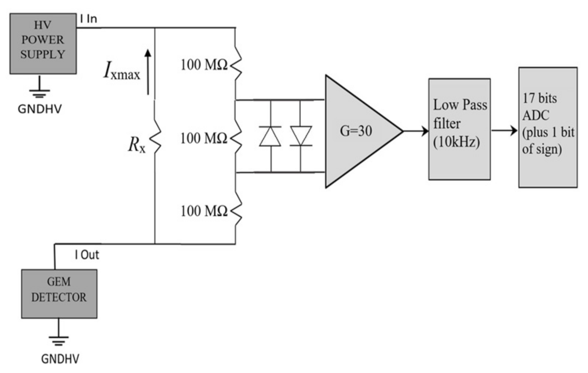
The instrument is easily scalable if it is necessary to connect more ammeters to cover a wider range; the limitation depends on the number of terminals available on the FPGA board and the modification of the FPGA control firmware would be a simple task. Each ammeter consists of a voltage source with a floating ground through a MED-FS16U-1512D DC-DC converter, a 17-bit LTC2326-18 ADC plus 1 sign bit to read data at a rate of 1 kHz, and four OPI1268S optocouplers with high-voltage insulation up to 20 kV. The three ammeters are identical using the same Printed Circuit Board (PCB) design, it is presented in
Figure 2.
The scale depends on the value of a single resistor. To protect the amplifier and the ADC from short circuits in the detector a resistive array is implemented, which consists of a resistance connected in parallel to 3 resistors of 100 MΩ in series. In this way the protection of the current monitor is secured. The current produces a voltage of , resulting in a voltage at the entrance of the amplifier. The value of is limited to 1 V. Therefore, the maximum voltage through the 100 MΩ resistor connected to the input of the amplifier is limited to 0.33 V in normal operation. This voltage is smaller than the direct polarization voltage of the protecting diodes. In case of accidental short circuits that would result in applying the full voltage to the resistances the sequence of events is the following: the of 1 W would burn while the three 100 MΩ resistors resist the load. In that case the diodes, depending on the polarization, effectively limit the voltage seen by the amplifier to +/−0.7 V, resulting in an amplifier saturation output voltage of +/−10.5 V.
3. Prototype of the Current Monitor
The main components of the current monitor used for the prototype in this work are presented in
Table 1.
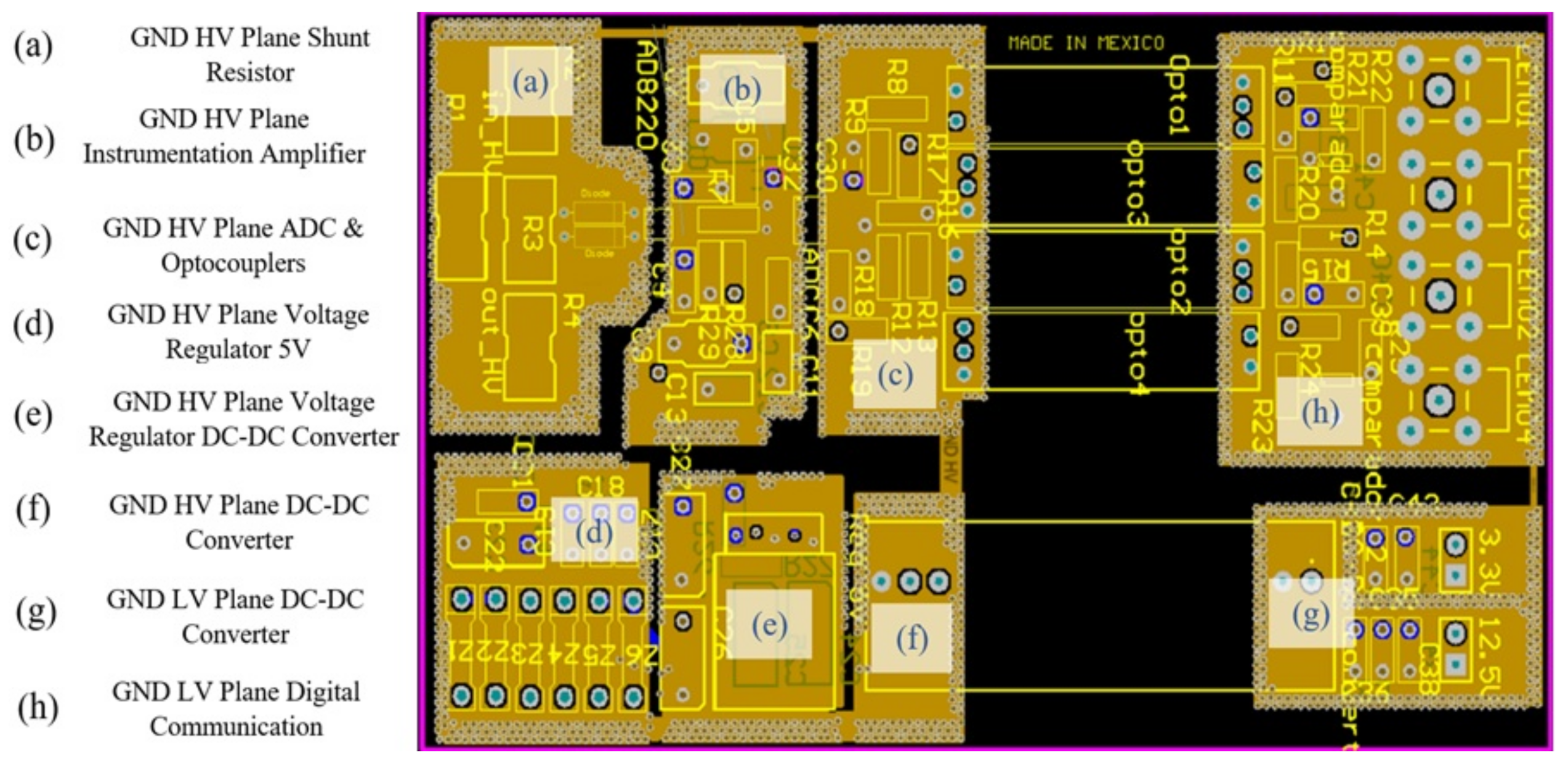
For the design of the PCB, several techniques were implemented to reduce the levels of electromagnetic interference (EMI). These strategies were the segmentation of the ground planes for the high (GND HV) and low voltage (GND LV), the use of vias around these planes, and the use of 100 nF capacitors between the power supply and ground terminals. The purpose of the vias is to form a shield to attenuate the EMI from the digital signals of the ADC and the DC-DC converters to the analog part of the circuit. Each plane shown in
Figure 3, where the planes (a–f) are connected to the high-voltage ground (GND HV) and the planes (g,h) are connected to the low-voltage ground (GND LV).
The scale resistor
, the protection circuit by the three 100 MW resistors, and the diodes are placed on top plane (a). The instrumentation amplifier is mounted between planes (a,b), in order to reduce EMI, and a low-pass filter of 10 kHz is mounted on plane (b). Four signals are used to drive the ADC from the FPGA. To isolate the FPGA from high voltage, 4 optocouplers are used to send and receive the 4 signals. The optocouplers are located on the bottom between plane (c,h). The low voltage power supply for the DC-DC converter is mounted on the top plane (g). The DC-DC converter is mounted on top between planes (g,f), the +/−12 V outputs of the DC-DC converter are on top plane (f), and finally the voltage regulator circuit that produces the +5 V is mounted on the top planes (d,e). All the ground planes (GND HV) are connected by a narrow trace in order to reduce the EMI between these planes, in the same way, all the planes (GND LV) are connected by a narrow trace too,
Figure 3 are illustrated. Furthermore, vias were distributed around each ground plane to produce an electromagnetic shield in order to reduce EMI among all the planes as shown in
Figure 4a.
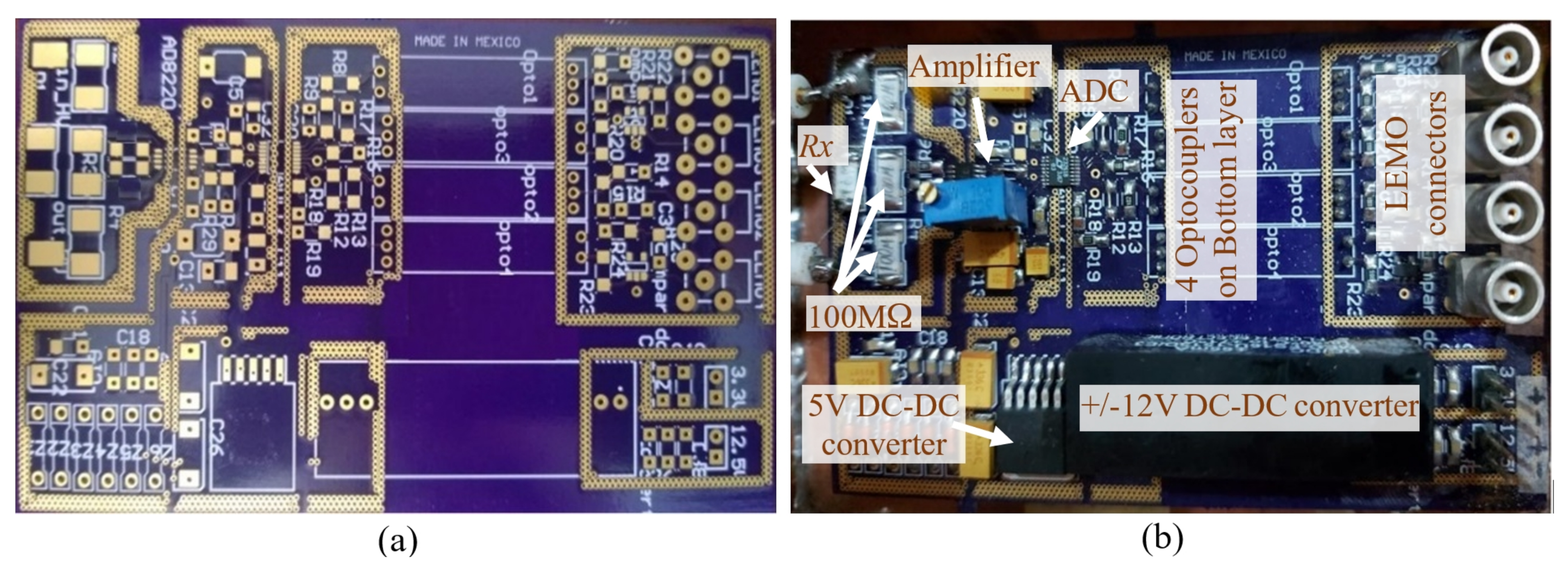
Figure 4b presents the components mounted on the top layer of the PCB. The optocouplers are mounted on the bottom layer of the PCB. On the other hand, the PCB design was made in ALTIUM DESIGNER
® software following the IPC-2221B and IPC-9592B standard regulations for high-voltage design.
To receive the data and process them, an own interface was developed using the NI LabVIEW
™ software, such as in the left side of
Figure 5, which displays the data in real-time in the graph, and the right side displays the smoothed data obtained averaging in succession using the last 40 samples taken in real-time. We used NI LabVIEW
™ for this work because it is possible to build a user interface simultaneously during the development of the program. Although, likewise, the program can be developed in any other software. NI LabVIEW
™ is a commercial software but it has the advantage of allowing to compile the program and produce an executable file (.exe) which can be run on any computer without the need to have NI LabVIEW
™ installed. The WiFly module allows the data reading to be transmitted in real-time to the PC via WiFi. However, the module has the option to send the data reading in real-time over the Internet so it can be stored in a cloud or shared with some other device, even though the data could be visualized in an app for mobile devices or on a website.
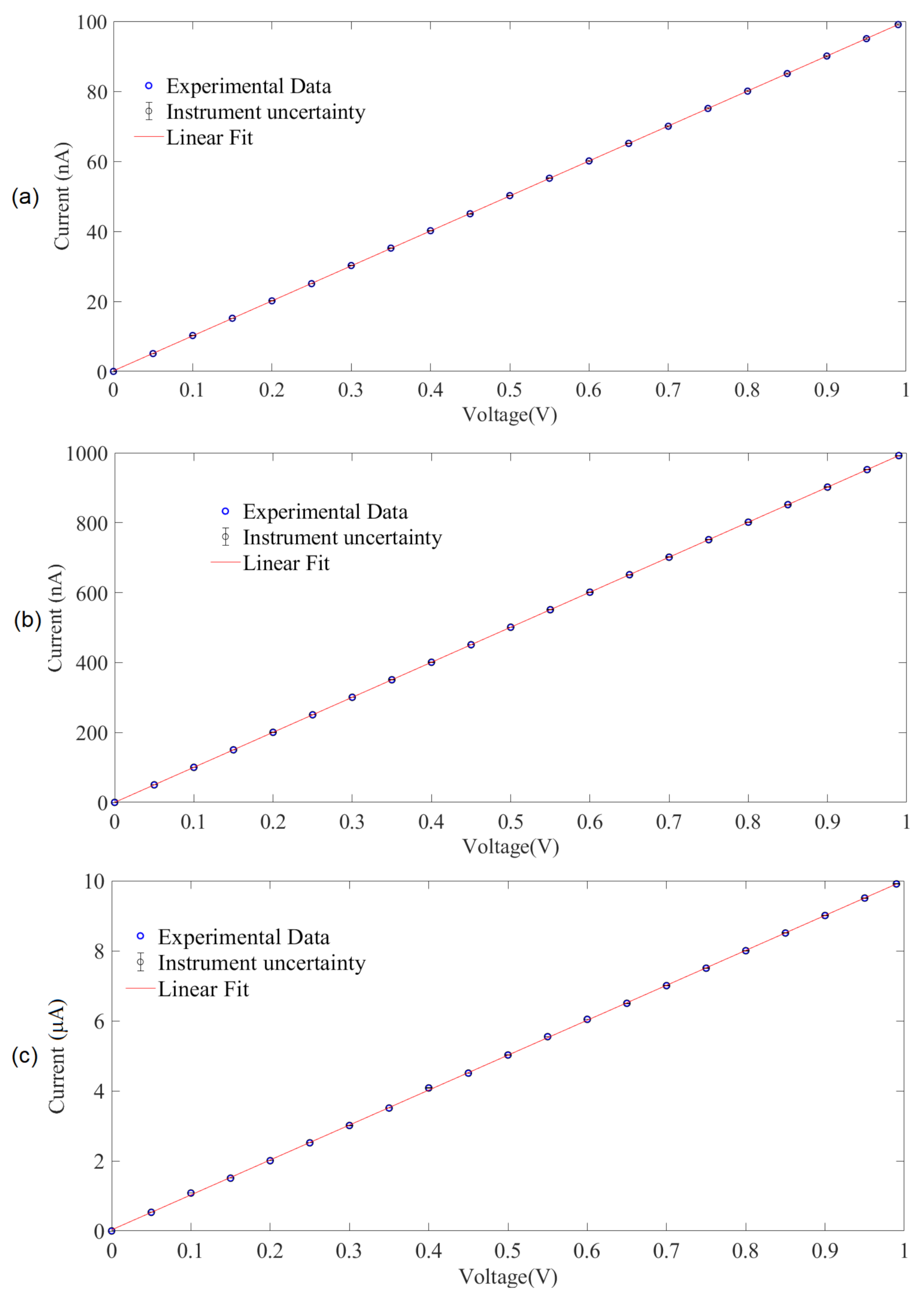
The calibration of the ammeters was carried out separately, each one according to its scale as can be seen in
Figure 6. The three ammeters were connected in series within the current monitoring system. The experimental setup uses a variable power supply connected in series with a commercial ammeter, Keithley
® 6514 certified from Aurora Road, Cleveland, OH, USA; in which the instrument is calibrated and accredited by the DIN/ ISO 17025:2005, DIN/ISO 17025:2017 and performs the work in accordance with its quality requirements and national standard ANSI/NCSL Z540-1-1994 (R2002) in the field of calibration [
19]. This device is connected in series with the
resistor scale included in the corresponding ammeter.
The calibration procedure of the ammeters is the following. Current was made to flow through the resistance
of a single ammeter and, simultaneously, this current
I(nA) was measured including its uncertainty
I(nA) with the commercial Keithley
® 6514 certified from Aurora Road, Cleveland, OH, USA. Therefore, this procedure is repeated for each ammeter, one at a time. To produce this current, it is used a power supply, its voltage was varied at regular intervals from 0 to 0.99 V with steps of 0.05 V, generating 21 experimental points for each ammeter, as shown in
Table 2.
Thus, the results of the calibration in the three ranges are shown in
Figure 7a–c, where the experimental value of each of the three
is determined, with which the calibration adjustment was made so that the currents of the reference instrument and those of each ammeter were equal, according to their scale. The value of the slope
m and its uncertainty
was obtained from the linear fit [
20], one for each ammeter. Then, for the first ammeter (0–100 nA), a slope of 99.8987 nA +/−0.0519 nA was obtained; for the second (0–1
A), a slope of 10,002.005 nA +/−0.003 nA; and finally, for the third (0–10
A), a slope of 9.9773
A +/−0.0175
A. The slope value was used to obtain the experimental
for each ammeter,
. The experimental values were an
of 10,010,236
for the 0–100 nA scale ammeter, the second of 997,999
for the 0–1
A scale ammeter and the third 100,227.5
for the 0–10
A scale ammeter. To obtain the percentage uncertainty, the standard deviation of the slope is divided by the value of the slope and this result is multiplied by 100%. For the 0–100 nA scale, the ammeter has an uncertainty of +/−0.05%; for the 0–1
A scale, the ammeter has an uncertainty of +/−0.003%; and for the 0–10
A scale, the ammeter has an uncertainty of +/−0.17%, according to the requirements of Sections 5.2.1, 5.2.3.2, and 5.2.3.3 from the IEC 60051-2:2018, [
21].
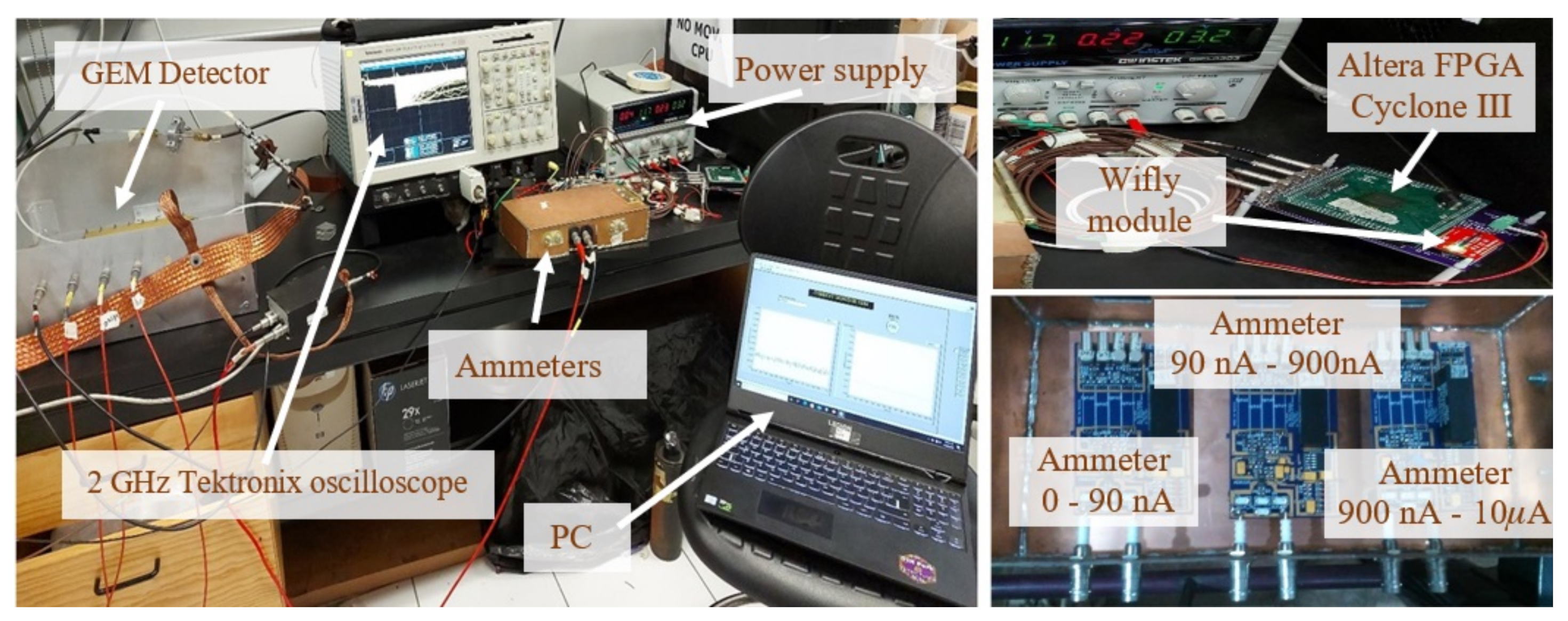
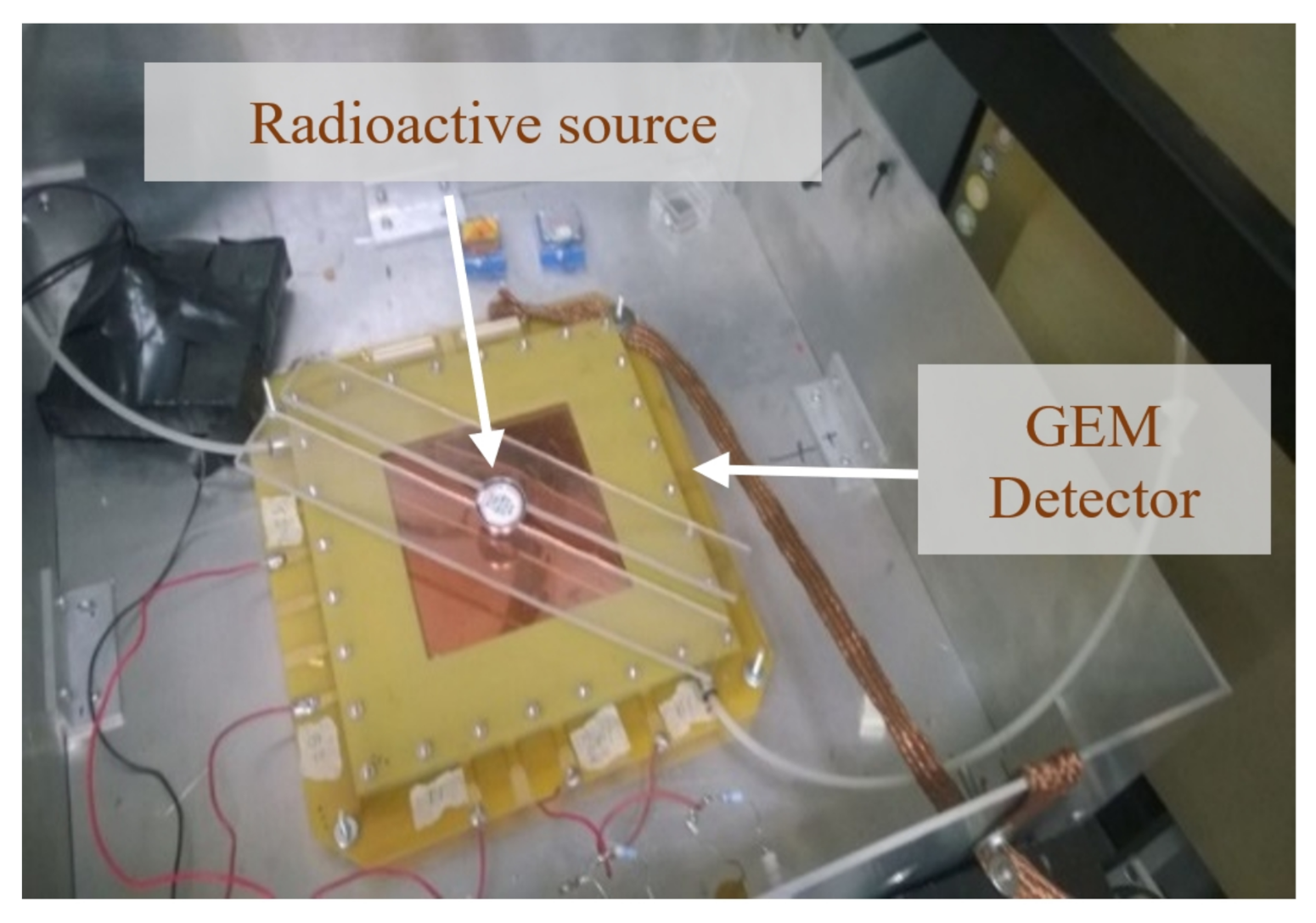
The complete experimental setup is shown in
Figure 8. Therefore, to test the current monitor, it was connected to a GEM detector. The three ammeters were placed inside a box made of double-sided printed circuit board to form a Faraday cage to decrease the external EMI.
4. Experimental Results
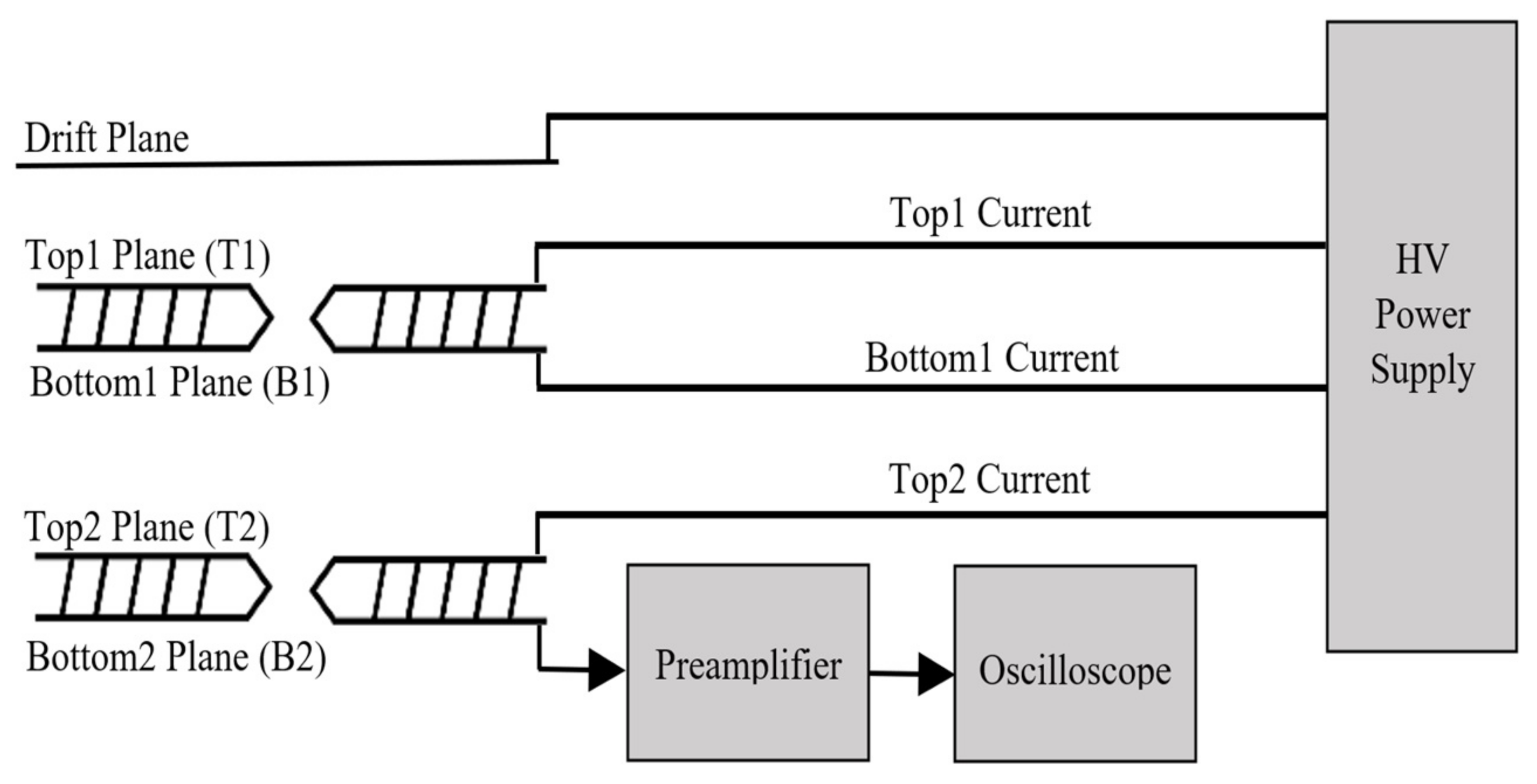
Tests were made to measure the current in different layers of the GEM as illustrated in
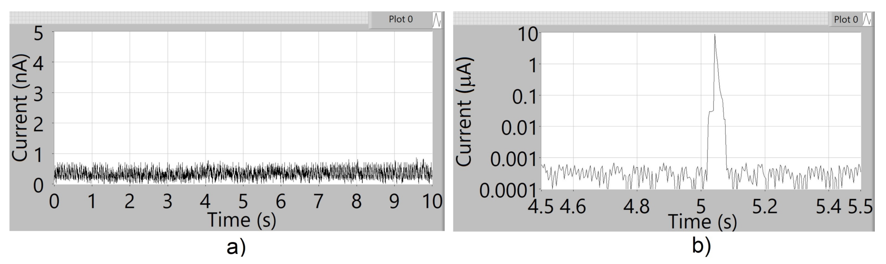
Figure 9. The GEM used has 5 layers: DRIFT, TOP 1, BOTTOM 1, TOP2, and BOTTOM 2, and the current was measured in three layers: TOP 1, BOTTOM 1, and TOP 2. Below we show the measurements in these 3 layers of the ICN-UNAM GEM. The current monitoring system was connected successively to the T1, B1, and T2 electrodes to measure the currents: in the stable regime (no discharges), the behavior under discharges, and finally measured with a radioactive source (Fe 55).
To show the whole range of the monitor we created discharges with a current in the order of microamperes. The results of the measurements in different electrodes are shown in
Figure 10,
Figure 11,
Figure 12, where results show that the ammeter performs with a maximum resolution for every current range thanks to the three-ammeter-in-one design. The ammeter operates in two different modes, i.e., it involving a single ammeter as can be seen in the figures on the left and the whole range covering from the noise in nanoamps to the spark currents in the Microamp range.
Finally, the response of the ammeter to a feeble source of iron 55 (Fe-55) of 78.63 kBq in the center of the GEM, and the response to the radioactive source, respectively, are shown in
Figure 13 and
Figure 14. Thus, a picture of the GEM´s detector is provided, as well as show the ammeter’s response which was produced by the radioactive source in which displays an increment in the current, from 290 pA to 580 pA as expected.
Table 3 summarizes the research results of evaluating the responses of current in GEM for each layer. As we can see from this table the current discharge in TOP1 is positive, in BOTTOM1 is negative and in TOP2 is positive. The current in stable state in TOP1 is 750 pA, in BOTTOM1 is 220 pA, and in TOP2 is 290 pA; in these cases, there is no radiation source. The current response in GEM TOP1 and BOTTOM1 is the same with and without a radiation source; meanwhile, the responses of current in GEM TOP2 change from 290 pA to 580 pA.
6. Conclusions
A self-adjusting current monitoring system with a range from picoamps to 10 microamps with a 1 kHz readout was developed, using some techniques to reduce electromagnetic interference:
These techniques were essential to the operation of the current monitor. Notably, we were able to use optocouplers to insulate the digital part from the analog one at high voltage. Furthermore, we were able to implement the DC-DC converters to power the electronic components in the high voltage part, in spite of the important interferences they generate. The details of the design (the segmentation of the ground planes and the inclusion of electromagnetic shields in the form of vias) allowed for a considerable decrease in the interferences. The three-in-one design allows having a self-adjusting range with the optimum resolution in each range. The readout at a frequency of 1 kHz and the possibility to have a smoothed plot were implemented.
The data reading is transmitted in real-time to a PC. In future work, we may configure the module to transmit the data read in real-time via internet (IoT), which would allow the data can be stored in a cloud or shared with some other device. The data could be visualized in an app for mobile devices or on a website.

 ,
, 


