


Abstract
Miniature spectrometers provide promising potential for on-chip or in situ optical analysis. In recent years there has been significant progress towards reducing the size and improving the performance of these spectrometers. The workhorse is light splitting components. This work has been led primarily by the innovative use of new light analysis strategies and new nanostructured materials with the notable increase in the spectral range and resolution. This review summarizes the latest developments classified as monochromatic, modulated and computational types of miniature spectrometers according to the spectral extraction methods. Particularly, we highlight the recent advances in designing of sophisticated gratings, resonators, interferometers and photonic crystals (PCs), the emerging of novel nanostructured materials and improvement in the computational spectra reconstruction algorithms. We examine the different approaches employed to reduce size and enhance light–matter interaction of the final spectrometers, especially emphasizing the trade-off between various metrics of the spectrometer including device footprint, measurable spectral range, spectral resolution, sensitivity as well as complementary metal oxide semiconductor compatibility. We also examine potential applications of on-chip spectrometers and outlook where further developments are required.
Export citation and abstract BibTeX RIS

Original content from this work may be used under the terms of the Creative Commons Attribution 4.0 license. Any further distribution of this work must maintain attribution to the author(s) and the title of the work, journal citation and DOI.
1. Introduction
Spectrometers are widely used tools in chemical and biological sensing, materials analysis and light source characterization [1–3]. Conventional spectrometers mainly consist three parts: light source, light splitting and detection components. They are bulky instruments often involving mechanical moving parts including gratings [4], mirrors [5], which severely compromises their deployment versatility and increases cost. Compact, lightweight, and rigid miniature spectrometers are greatly needed for a wide variety of applications. For example, handheld devices and smart phone-based chemical analysis application in environmental sector (e.g. water and food analysis), biomedical applications (e.g. blood, plasma, urine analysis, etc), industrial operations, homeland security and so on. Miniaturization also paves the way for making in situ measurements such as spectroscopic sensing, optical network performance monitoring [6], hyper-spectral imaging [7], and radiofrequency spectrum analysis [8]. It eases the integration of microspectrometers and miniature spectrometers into other technologies, such as microelectronics, and helps to realize lab-on-a-chip devices and very large scale integrated systems. In the latest decades, there reported substantial miniaturized and on-chip spectrometers in the academia and industrial circle.
Miniature spectrometers employ waveguide or fiber guiding incident light to a dispersive component with different light splitting methods, then discriminated light is directly projected or transmitted through couplers to a detector or detector array, and finally signals are recorded and reconstructed computationally. Small lasers are reviewed by Gather in [9]. As well as, over the past two decades, great progress have been achieved in the miniature spectrometer by using different light splitting and detection methods combined with spectral reconstruction algorithms. The spectrometers in general can be classified as, monochromatic dispersive type or wavelength multiplexing principle type, according to the volume of light–matter interaction.
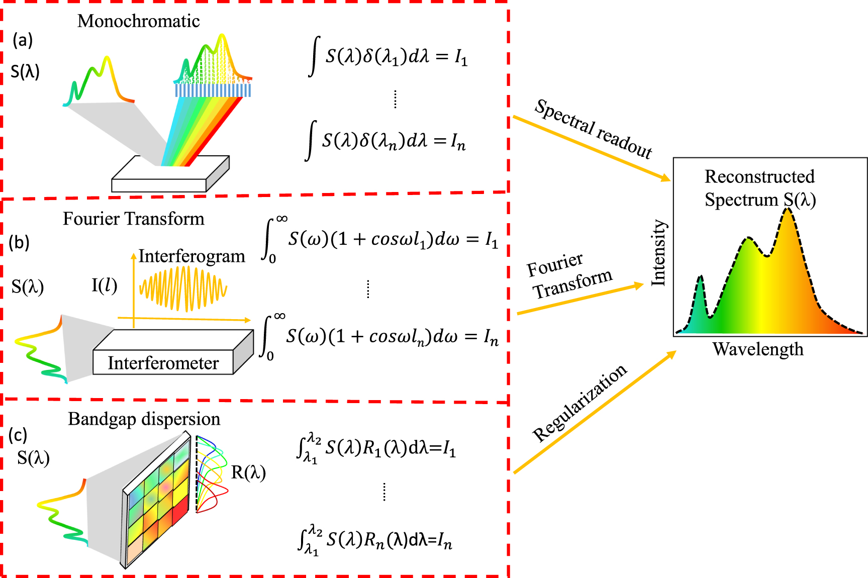
Figure 1 schematically illustrates strategies for miniature spectrometer according to light–matter interaction strength, including light splitting methods and spectral reconstruction algorithms. Figure 1(a) shows the monochromatic dispersive light splitting method, it uses optical component such as gratings [10–12], narrow band filters [13, 14], micro-resonator array [15] to produce monochromatic light recorded by

Figure 1. Schematic illustration of different miniature spectrometer mechanisms. (a) Monochromatic dispersive grating-based spectrometer, light is discriminated and projected to detector array, incident light spectrum is readout by a computer simultaneously. (b) Wavelength multiplexing by using interferometer to have interferogram in spatial or time domain, spectrum is constructed through Fourier transform process. (c) Wavelength multiplexing by using bandgap dispersive filters with different broad-band transmission spectra, the originally spectrum is reconstructed from the intensities detected from each broadband filter.
Download figure:
Standard image High-resolution imagedetector array, incident light can be restored by using delta-like functions readout spontaneously by a computer. An alternative approach uses wavelength multiplexing [16] component such as Fourier transform interferometer or a set of distinct, yet continuously tunable, broadband filters as illustrated in figures 1(b) and (c), respectively. The former employs interferometer such as Michaelson interferometer [5], Lippmann's interferometer [17] Mach–Zehnder interferometer (MZI) [18] or Febry–Perot interferometer [19] to obtain interferogram in time or spatial domain, spectrum can be reconstructed by sinusoidal functions as Fourier transform process. The other one is called bandgap dispersion due to that this kind of light splitters have a band or band-like structure allowing light selection as well as wavelength multiplexing, such as PC slab [20] or nanostructured semiconductor [21, 22], and finally the target spectrum will be retrieved from the set of measured broadband intensity distributions by regularization functions.
First and foremost, let us make clear the limitation on size scaling. There are several metrics to evaluate the performance of the miniature spectrometers, including measurable band width (BW) and dynamic spectral range, spectral resolution or resolution power (R), sensitivity (S), scalability and so forth. Furthermore, to analyze how miniaturization affect the performance, taking the grating-based spectrometer for example, both the measurable SR and R depend on the optical path length (OPL):  , k is diffraction order, and N is the number of grating grooves; the spectral range is determined by the optical path difference (OPD), that is related to k and corresponding diffraction angle
  , as
, as  , where a and b are the grating constants. The measureable spectral range
  is proportional to the differential angle of the same diffraction order, the higher of k (indicating larger OPD), the broader BW and higher R, however, higher diffraction order k resulting in greatly reduced light intensity. For miniature spectrometer by using micro-sized grating into a chip scale platform, compromise often the R and BW for its limited space. Similar behavior of R and BW for spectrometers employs interferometers. The other key factor is sensitivity, which is related to the light–matter interaction strength, let us take it as:
 where
where  is the incident light flux normal to the detector. With the shrinkage of the size of spectrometer, the incident light flux is dramatically decreased, sensitivity will become a great challenge for a compact, especially, on-chip spectrometer.
Over the past few decades, microspectrometers realized by using silicon process compatible technologies, low-cost batch fabrication of an intelligent optoelectronic system-on-a-chip are feasible by integration of optics with microelectronic circuits [23], such as concave or mini-gratings [11, 24, 25], waveguide array [12, 26, 27] and Fabry–Perot cavity array [19]. However, the spectral resolution of devices presented so far has been limited to about 10 nm due to limited free OPL, which severely limits application. Most recently, the development of the advanced photonic engineering and manufacturing technologies enable fabricating complex structured optical components and thus facilitating miniature spectrometer with better performance available. A compact spectrometer with integrated filter array whose size is 12 mm × 12 mm demonstrated 1.7 nm in R and 158 nm in measurable BW [13]. Spectrometers employ digital planner hologram (DPH) grating [28–30] with longer OPL can have fine R of 0.15 nm and broad BW of 148 nm, what's more the total device footprint is below 2 cm2. Micro-rings and micro-resonators can also enable fine resolution [15, 31]. Super fine R of 30 pm was achieved by using random scattering PCs [32] (with radius ∼ 100 μm) which can fold the OPL by random scattering, as well as exhibit a broad BW of 128 nm with a 'satisfying' spectral resolution of 4 nm as a trade-off. Conventional infrared spectrometer usually employ an interferometer with moving mirrors to modulate the OPD to create interferogram for different wavelength, alternative approach is using stationary standing wave interferometer [17, 33] by recording near-field intensity of [17] different wavelength; particularly, an integrated single-waveguide Fourier transform spectrometer exploits electro-optic properties of thin film lithium niobate (LN) to change the optical material index to get modulated OPD, and demonstrated a resolution of 4 nm and operation BW of 500 nm in the near and short wave infrared with a footprint of less than 10 mm2. A novel digital Fourier transform (dFT) on-chip spectrometer exhibits scalability by using digital controlled optically choosing MZI with different OPD with super fine resolution of 25 pm. Based on wavelength multiplexing principle, unlike monochromatic component allowing only a small amount of light transmission, a unique broadband transmission filters was used as light discrimination components to improve the sensitivity and have broad dynamic operation BW, such as PC slabs filter array [20], colloidal semiconductor quantum dots filters array [22], miniature spectrometers as bandgap gradient CdSx Se1−x single nanowire spectrometer [34, 35], silicon nanowire array spectrometer [21, 36].
The size and resolution have been greatly improved for the emerging miniature spectrometer. However very rare work contributes to real in situ monitor of on-chip light emitting measurement. As on-chip measurement is a complex light–matter interaction process and usually undertakes weak signal detection, which requires the spectrometer with high sensitivity. Among them, spectrometer with DPH grating can detect 50 pm nm−1, that using disorder PC or echelle gratings equipped with superconducting nanowire detector working @ 1.5 K can detect single photon. It is worth noting that, Wang et al carefully engineered the CdSx Se1−x nanowire to a waveguide-mode-operated, dispersive Schottky diode photodetector array, enabling a monolithic spectrometer chip with strong light–matter interaction and superior noise figure of 1013Jones and carried out on-chip photoluminescence (PL) measurement with R of 5 nm.
In this Review we discuss the recent progress towards ever more compact spectrometers. Each type of spectrometer uses a particular strategy to address the fundamental challenges involved in reducing device size and enhancing light–matter interaction. First we examine the key spectrometer characteristics that result from each strategy, and identify applications that benefit. We then discuss the challenges ahead towards further miniaturization and obtaining devices that are useful for commercial and practical applications.
2. Miniature spectrometer strategies
2.1. Monochromatic dispersive miniature spectrometers
The core component of conventional monochromatic spectrometers is a dispersive optical element, such as diffraction gratings. Light is guided to a mechanistically-control grating by a series of mirrors, after that it is split into monochromatic light distributed in space where different position corresponding to different wavelength, and detected by a detector in time domain or by detector array simultaneously [37, 38]. These spectrometers can reach ultrahigh resolution and have broad spectral ranges, available high-performance multiple-grating macroscopic spectrometers feature an impressive spectral resolution exceed R = 0.1 pm [39], but their excessive footprint and portability limit their applicability. With shrinkage of the spectrometer, performance drops as the device footprint becomes smaller, which generally results in a decrement of resolution or spectral range due to limited OPL. Researchers take advantage of advanced photonic integration technology and new nanostructure material fabricating delicate optical structures to improve its performance. Integrated spectrometers based on arrayed-waveguide gratings [10, 12, 26, 40], PC [41], silicon spiral waveguides [42], micro rings [43] and microdonut resonators [44] (as some of them are shown in figure 2) can reach relatively high resolutions, but their spectral range is narrow and often constrained by the number of output waveguides. Approaches that use planar diffraction gratings [10] and echelle gratings [11, 24] are also capable of high resolution, while their working range is mainly limited by their free spectral range. On the contrary, spectrometers based on micro-electromechanical systems [45], filter arrays of Fabry–Perot cavities [19] exhibit broad spectral ranges but have a poor resolution. Each of the aforementioned approaches is also not sufficiently resilient to fabrication errors. This problem encouraged the development of a high-resolution spectrometer based on disordered scattering media [46]. Instead of fine R of sub-nanometer is demonstrated, this solution is not flexible and can only work on a narrow spectral range and can satisfy some specified applications.

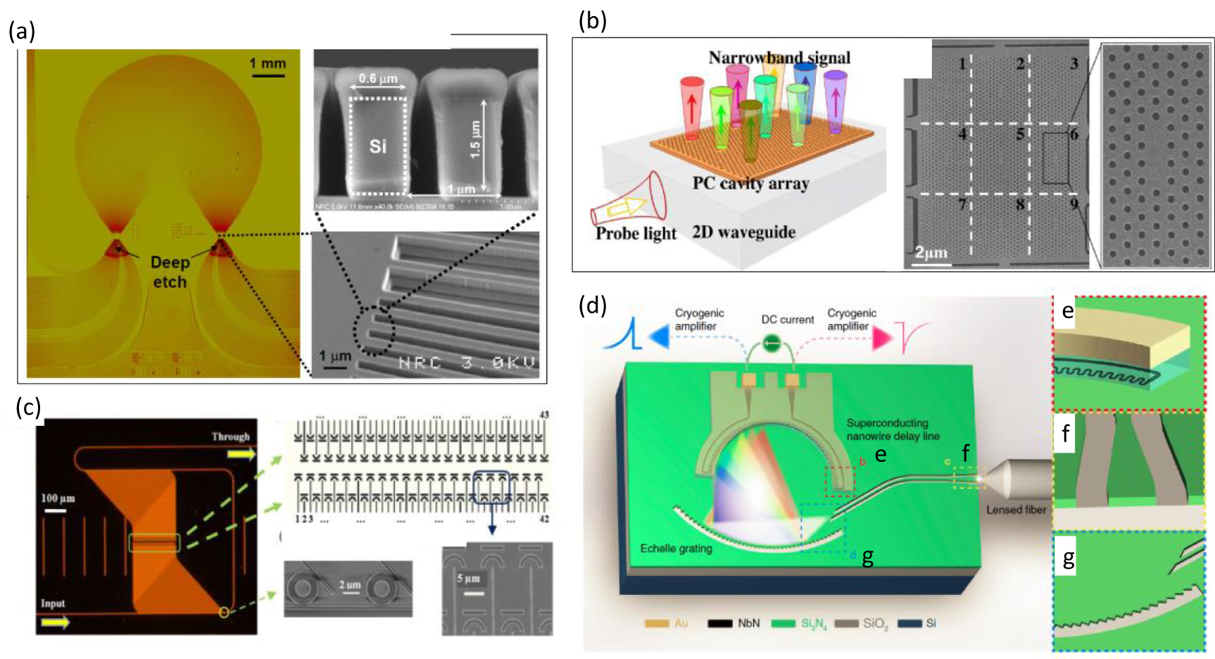
Figure 2. The typical micro-monochromatic light splitting component. (a) An optical microphotograph of a 100-channel silicon on insulator arrayed waveguide grating (AWG) spectrometer and its scanning electron microscopy (SEM) images. (b) Schematic of the compact spectrometer based on a planar PC (PPC) cavity array coupled with a 2D waveguide, and SEM images of a fabricated PPC cavity array; (c) Micrograph of the spectrometer with microdonut resonators array, its 2D array of the scatters with channel numbers labeled and the SEM image of two microdonut resonators coupled to the input waveguide and the SEM image of a portion of the 2D array of the scatters. (d)–(g) 3D sketch of the device of the on-chip focusing echelle grating operates as wavelength-discriminating micro-photonic component while the superconducting nanowire functions simultaneously as a single-photon detector (SCD) [15, 41, 42, 47].
Download figure:
Standard image High-resolution imageMeanwhile, some remarkable progress has been done recently. By integrating an on-chip dispersive Rowland circle echelle grating with a single element propagating superconducting nanowire detector, the first broadband chip-scale single-photon spectrometer with R less than 7 nm covering both visible and infrared wavebands spanning from 600 nm to 2000 nm was realized by Hong X Tang [32] as shown in figure 2(d). New structure like random scattering DPH grating [30] as well as disordered random PC [46] greatly enhance the OPL of miniature spectrometer resulting in extremely fine R and broad BW. That employed mini-filter array [13] with multilayers demonstrated very narrow transmission band and realized R = 1.7 nm and BW over a 158 nm, which is smaller than 1 cm3. Not only the new structures, the new nanomaterial can also give narrow transmission spectra combined with algorithm process. Bao et al fabricated 195 unique filters array with colloidal quantum dots [22] and realized a compact spectrometer with R = 2 nm and BW over a 300 nm, which is comparable with a US quarter.
The following are some state-of-the-art typical broad-band monochromatic based miniature spectrometers with remarkable performance merits with discussion in details.
2.1.1. Digital planar hologram grating on-chip spectrometer
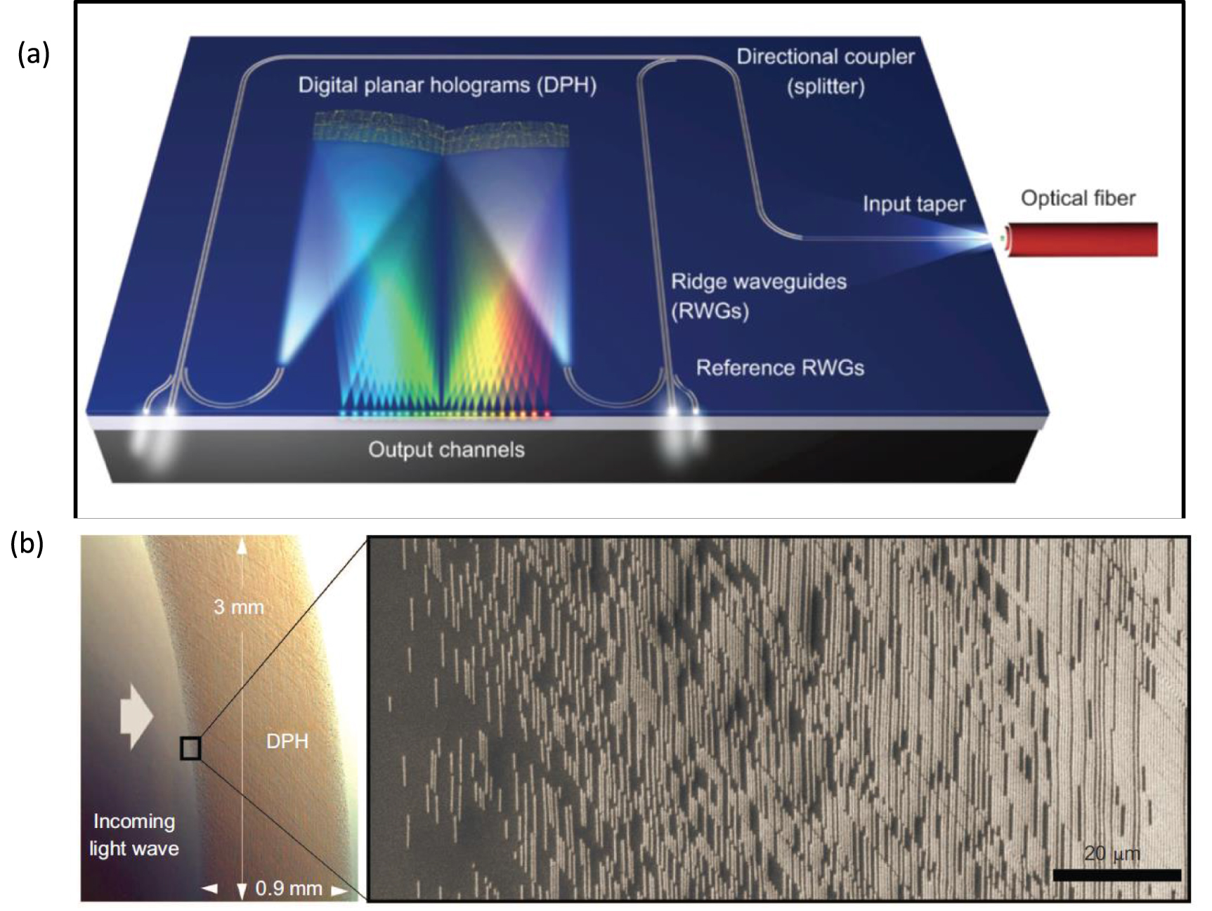
As we know that the great challenge coming from shrinkage of spectrometer is the limited OPL resulting in poor R and SR, which are two very important metrics for a spectrometer. DPH grating is a new approach for designing devices with the programmed properties to control light scattering many times to gain longer OPL [28–30]. This technology belongs to the class of computer generated holograms and can encode any specific optical transfer function by manipulating the light in the spectral and spatial domains. DPH involves millions of lines specifically located and oriented in order to direct the output light into the designed focal points according to the wavelength as illustrated in figure 3(a). Spectrometers were fabricated on dielectric material such as silicon nitride or silicon dioxide or hafnium dioxide planar waveguides using electron beam lithography (EBL) and dry etching, a typical linewidth of grating's grooves was 100–140 nm linewidth and 50–150 nm depth for SiO2Gex waveguide core, and about 80 nm linewidth and 10–20 nm depth for devices with HfO2 core as shown in figure 3(b). Each DPH works in one specific spectral bandwidth, whereas the integrated circuitry includes several functionalities (taper, splitter, and waveguide) to efficiently manipulate the light and guide it to the holograms. Integration multiple DPHs on the same device can broaden the measurement spectral range. In this way a high-resolution, broadband spectrometer-on-chip can be realized with performance that is similar to conventional spectrometers. In 2014 [30], the newly developed spectrometer achieved a high spectral resolution of 0.15 nm in the red and near infrared range, over a 148 nm spectral range (630–694 nm, 766–850 nm) with 926 channels, while maintaining the total device footprint below 2 cm2. In addition to the bandwidth and linewidth, the dispersion curve of a DPH spectrometer can be customized to assume any specific profile, allowing resolution changes over different bands of interest for specific applications. While the spectral range is mainly limited by the number of channels. Another disadvantage is the scattering loss (is around −15 dB) and the Cross-talk (defined as the ratio between the light intensity in one channel and the intensity of the interfering light in lateral channels ∼10 dB) along light propagation. Despite the loss, an input spectral intensity as low as 50 pW nm−1 can be detected with an integration time of 10 ms. For practical application, high quality of structure with small roughness is highly desired to reduce the optical loss. And the requirement will become stricter for application in light with shorter wavelength for the finer nanostructure of DHP grating should be fabricated.

Figure 3. (a) Schematic of an integrated DPH spectrometer. The spectrometer-on-chip integrates one or multiple DPHs and optical circuitry for coupling and wave-splitting operations. The light is brought to the chip with an optical fiber and coupled through a planar taper; light is guided with low losses by ridge waveguides and split based on its bandwidth by directional couplers; once directed to the hologram operating in the relative band, light is demultiplexed and focused on several different output channels at the edge of the chip. (b) DPH spectrometer fabrication details. DPH, digital planar hologram [30].
Download figure:
Standard image High-resolution image2.1.2. Miniature spectrometer with mini-filters array
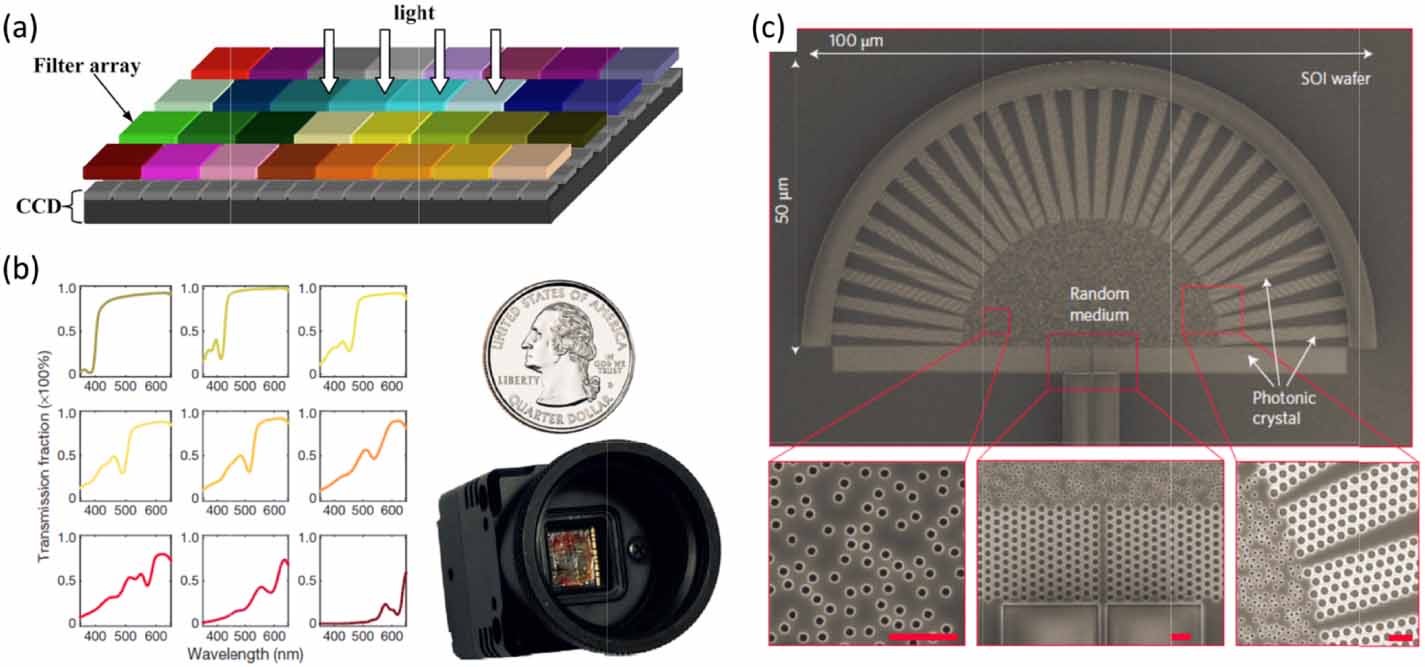
Narrow-band pass filters are another important monochromatic dispersion component, modern optics engineering lay the foundation for complex components fabrication, such as plasmonic metal array and dielectric mini-filters array. A high-resolution miniature spectrometer with 128-channel integrated mini filter array has been demonstrated in 2007 by Lu et al [13] schematically shown in figure 4(a) with ultra-narrow transmission spectra. These filters were fabricated by using the combinatorial deposition technique to deposit film layers to form Bragg-cavity with selected wavelength, and work as a dispersive component whose passbands range from 722.0 to 880.0 nm with a bandwidth (or spectral resolution) from 1.7 to 3.8 nm. The miniature spectrometer is smaller than 1 cm3. Total pixel number is 795 × 596 with each pixel size of 6.5 μm × 6.25 μm, is just put in front of a charge-coupled device (CCD) camera, without any moving parts. Incident light propagate through the ultra-narrow band-pass filter to form monochromatic light and detected by the CCD underneath at different location, then the signals are collected by computer to form a continuous spectrum. This kind of miniature spectrometer has the advantages of very low payload, high resolution. But the complex fabrication process and small amount of incident light on each filter make the sensitivity a great challenge.

Figure 4. (a) Schematic diagram of a compact spectrometer composed of the 128-channel integrated filter array and a CCD; (b) transmission spectra for some of the CQD filters and a microspectrometer in the form of a digital camera with electronics and circuits, made from the 195 CQD filters and a CCD array detector, which is comparable in size to a US quarter; (c) the SEM image of a chip-based spectrometer based on multiple scattering in a disordered photonic structure. The dispersive element is a semicircular array of randomly positioned air holes, surrounded by a PC lattice [13, 22, 46].
Download figure:
Standard image High-resolution image2.1.3. Compact spectrometer employing semiconductor colloidal quantum dots as filter array
Most current microspectrometers rely on interference filters and interferometric optics that limit their photon efficiency, resolution and spectral range. Bao and Bawendi have developed an efficient, cost-effective microspectrometer that overcomes many of these limitations by replacing interferometric optics with a 2D absorptive filter array consisting of 195 different semiconductor colloidal quantum dots array with transmission features that cover a broad spectral range [22], figure 4(b) gives the typical transmission spectral of colloidal quantum dots (CQDs) and the device picture. With it the authors reconstructed spectra with R of 2–3 nm and broad BW of 300 nm, where R is related to the variation of the CQDs size and BW is determined by the optical properties of intrinsic semiconductor material. The dynamic spectral range can be extended to a quiet a broad range by using the other kind of CQDs such as ZnS or InP, respectively [48]. This approach gives a simple and easy way for a miniature spectrometer with high performance, especially potential higher R could be obtained by well controlled CQDs fabrication. But its operation spectral range depends on the semiconductor's property, as a result, a limited measurable spectral range. As well as basically, the delta transmission spectra contribute to the spectra reconstruction, this approach still does not improve the weak light–matter interaction strength caused by size shrinkage.
2.1.4. Compact spectrometer with PC filter
Photonic crystal nanocavity or random structure can function as monochromatic dispersion component. A compact spectrometer with an array of high-quality-factor PC nanocavities [49], coupled via a planar 2D waveguide enables spectral analysis of incident light with resolution as high as the bandwidth of the cavity mode –0.3 nm at 840 nm. Due to limited OPL, the BW is only about 20 nm with 100 cavities. Unfortunately, it is very sensitive to fabrication errors. In addition to these carefully designed systems, disorder and scattering system have also been explored for spectroscopy applications benefiting from its longer OPL [41, 49]. Early in 2003, Xu et al used the spatial-spectral transmission patterns induced on low coherent field by disordered PCs to construct multimodal spectrometers which are designed to measure the spectral density averaged over multiple spatial modes [50]. In 2010, Dogariu et al showed that random scattering materials have sufficient diversity in spectral transmission to allow for precise measurements of the spectrally dependent polarization state of an optical field [51]. In 2013, Cao et al used multiple scattering in on-chip random structure of semicircular (with radius of 25 μm) array of randomly positioned air holes [46] to build a compact spectrometer, which greatly increase the OPL and achieved fine spectral resolution of 0.75 nm and 25 nm bandwidth around 1500 nm with a small footprint. As shown in figure 4 (c). The incident light is guided by a waveguide then diffuses through the random array via multiple scattering and eventually reaches 25 defect waveguides which will couple the signals to the detectors array (not integrated). The distribution of intensities over the detectors is used to identify the input spectrum. But, losses coming from scattering and the out-of-plane leakage limit its sensitivity. By replacing the detector array with superconducting nanowire SCDs, most recently Pernice et al employed the similar random PC (with radius of 100 μm) structured spectrometer equipped with a SCD and realized high sensitivity down to powers of −111.5 dBm in the telecom band [32, 52]. They reconstructed near infrared spectrum with super fine linewidth of 4 nm and 30 pm (around 1500 nm and around 800 nm, respectively) and high sensitivity in 1.3 K ambient.
The working principle of such disordered PC devices is based on the analysis of the speckle pattern which is formed by light after propagation through a disordered medium. The speckle pattern provides a unique 'fingerprint', which is usually stored beforehand in a calibrated transmission matrix. This matrix contains the spectral-spatial-mapping of the spectrometer. By measuring this 'fingerprint', any probe signal can be reconstructed by inverse multiplication with the transmission matrix. There are two main advantages of this smallest spectrometer: fine spectral resolution can be achieved due to the greatly enhanced OPL; the other is the spectrometer can work in a broad dynamic spectral range determined by the calibrating spectra. However, this kind of spectrometer will be damaged if the probe light is out of the calibrating light. Meanwhile the limited number of output channels result in narrow BW for each measurement.
A summary of some remarkable monochromatic dispersive micro spectrometers is presented in table 1, with respect to device footprint, bandwidth, resolution, sensitivity and so forth.
Table 1. A summary of the monochromatic dispersive microspectrometers with key performance metrics.
| Configuration | Device footprint | Bandwidth (nm) | Resolution | Detector/Sensitivity related | CMOS compatible | Ref. |
|---|---|---|---|---|---|---|
| AWG | 8 × 8 mm2 | 1537–1557 | 0.2 nm | Detector array | YES | [42] |
| Spiral Waveguides | Radius = 250 µm | 545–725 | 20 pm | Detector array | YES | [41] |
| Grating prism | 11 × 11 mm2 | 350–650 | 9 nm | Detector array | YES | [10] |
| DPH grating | 2 cm2 | 630–694 & {7}66–850 | 0.15 nm | Detector array 50 pW nm−1 | YES | [30] |
| Concave grating | 1 × 4 × 3.7 mm3 | 750–1000 | 2 nm | Detector array | YES | [25] |
| Microdonut resonator | ∼cm2 | 1540–1610 | 0.6 nm | Detector array | YES | [15] |
| Mini filter array | 12 × 12 mm2 | 722–880 | 1.7–3.8 nm | Detector array | YES | [13] |
| Echelle grating with SCD | <1 cm2 | 600–2000 | 7 nm | Single Photon detection (@1.5 K) | +SCD NW Assembling | [47] |
| Disorder PC with SCD | Radius = 100 µm | 1530–1580/799–799.8 | 4 nm @1500 nm/30 pm @880 nm | −111.5 dBm (SCD @1.3 K) | +SCD NW Assembling | [32] |
| Disorder PC | 25 µm × 50 µm | 1500–1525 | 0.75 nm | Detector array SNR∼1000 | YES | [46] |
| CQD | ∼cm2 | 390–690 | 2–3 nm | Detector array | +CQDs painting | [22] |
2.2. Fourier transform based infrared micro spectrometer
Mid-infrared (IR) (2–20 μm wavelength range) is a technologically important wave band that encompasses multiple atmospheric windows (e.g. 3–5 μm and 8–14 μm) and covers the important absorption bands of most chemical molecules as well as the fingerprint region (7–20 μm), both of which are of great interest to spectroscopic sensing [47, 53]. However, mid-IR optical system are susceptible to the fluctuation of thermal for this band light having much lower photon energy, requiring different measuring system from their counterpart UV–Visible or near IR. Different from dispersive spectrometer, FTIR spectrometers overcome the trade-off between signal to noise ratio (SNR) and spectral resolution taking the advantage of wavelength multiplexing, also known as Fellgett's advantage [16]. Traditional benchtop FTIR spectrometers use moving mirrors to get a tunable OPL and recorded by one detector (infrared detectors like MCT are usually costly) in time domain to produce interferogram, spectra can be retrieved by Fourier transforming. Available high-performance commercial FTIR. Which is not easy to be integrated to planar photonic chip [54]. Prior work has demonstrated Fourier-transform spectrometers using planar waveguide array [55, 56], arrays of discrete MZIs [18, 47, 55, 57, 58] or spatial heterodyne Fourier transform spectrometer (SHFTS) [58] can achieve extremely high R but with BW ∼ 1 nm. Due to excessive chip footprints, these approaches are not practical for large spectral channel counts but only practical for sparse spectra such as laser lines. Furthermore, microring resonator-assisted Fourier-transform (RAFT) [44] spectrometer achieved R = 0.47 nm and BW = 90 nm, which was realized by using a tunable MZI cascaded with a tunable microring resonator (MRR), integrated with a photodetector onto a single chip as shown in figure 5(c). As well as micro-opto-electro-mechanical system (MOEMS) FT-IR System [59] is based on a classical Michelson interferometer design with the MOEMS mirror as the key element to change the OPL, which demonstrate a 4000–700 cm−1 at a spectral resolution of 13 cm−1. But the devices still have a large footprint and constrain the spectral resolution, far inferior compared to their benchtop counterparts. The above methods still need moving parts. Meanwhile, (dFT spectrometer [60] architecture that resolved the performance and scalability challenges with R = 0.025 nm and dynamic BW determined by number of parallel MZI and optical switches. As well as by using detectors array recording near field of standing wave of Lippman's interferometer, the footprint of spectrometer is greatly reduced to less than 10 mm2, further improved by using electro-optic LN waveguide, the spectrometer achieved an operational bandwidth of 500 nm in the near- and short-wavelength infrared.

Figure 5. Typical infrared miniature spectrometers. (a) and (b) Images and schematics of the dFT architecture. (a) Block diagram illustrating the generic structure of a dFT spectrometer with j switches and photo of the fully packaged, plug-and-play dFT spectrometer. (c) A schematic of the microring RAFT spectrometer consisting of a MRR and an MZI. (d) Stationary-wave integrated Fourier-transform spectrometry. (a) (left) In the Lippmann configuration, the forward propagating wave coupled in the waveguide is reflected on the mirror, leading to a stationary wave. If the light is polychromatic, the sum of the stationary waves forms a Lippmann interferogram. (right) Schematic of the near-field detection of the guided mode using a collection of nanodetectors. (e)–(g) Electro-optic sampling of the broadband interferogram under different voltages [17, 22, 44].
Download figure:
Standard image High-resolution imageHere we briefly introduce the most latest advanced method of Fourier Transform based on-chip spectrometers.
2.2.1. Scalable broadband on-chip Fourier transform spectrometer
Both the limited channel counts and moving parts are the challenges for FTIR spectrometers scaling down. In 2018, Hu et al proposed and experimentally demonstrated a novel dFT spectrometer architecture that resolved the performance and scalability challenges [60] by digitally controlling exponentially increase in channel counts. The device consists of two arms of MZI with number j optical switches on each arm that direct light to waveguides of unique path lengths illustrated in figure 5(a). And thus the channel counts increase by 2j . This approach claims three key advantages over state-of-the-art techniques. First, both the resolution and spectral channel count scale exponentially with j. The unique exponential scaling laws inherent to the dFT architecture enable high-resolution spectra to be acquired with minimal chip space and control electronics. Second, direct modification of the waveguide path offers over two orders of magnitude larger OPL modulation per unit waveguide length compared to thermo-optic- or electro-optic-based index modulation, enabling superior spectral resolution within a compact device. Third, the device benefits from the multiplex advantage and requires only a single-element photodetector rather than a linear detector array, which reduces cost and system complexity. They used this spectrometer with 64-channels (device picture is given in figure 5(b)) to restore a broadband spectrum from 1550 to 1570 nm with super fine resolution of 0.025 nm. The dynamic spectral range can be expanded by increasing the number of the switches as well as the length of MZI.
This work pioneers dFT spectroscopy as a high performance, scalable solution for on-chip optical spectrum analysis. Moreover, its proven compatibility with industry-standard foundry processes enables scalable manufacturing and drastic cost reduction. They further developed an elastic-D1 machine learning regularization technique to achieve significant noise suppression and resolution enhancement. The powerful combination of dFT spectroscopy and machine learning techniques will empower future applications of spectroscopy such as chemical and biological sensors-on-a-chip, space-borne spectroscopy, optical network monitoring, and radio-frequency spectrum analysis.
2.2.2. Stationary wave integrated Fourier spectrometer (SWIFT)
SWIFT working without any moving parts is promising for integration by analyzing light by standing wave, which was first proposed by Gabriel Lippmann in 1891, unfortunately, this principle was too complex to use, even though there has been great progress in more than one century [61]. In 2007, Coarer et al taking advantage of the development of photonics and near-field optics, proposed a new kind of stationary-wave integrated Fourier-transform spectrometry (SWIFTS) [17, 62], in which direct sampling of evanescent standing waves was achieved using a collection of optical nanoprobes of gold nanowires (named as evanescent field samplers (EFSs)) with 4  × 50 nm in size, around 3
  in space, illustrated in figure 5(d). Light is coupled into a single mode waveguide terminated with a mirror. When reflected onto the mirror, the waves become stationary. Miniature localized detectors are placed in the evanescent field of the waveguide mode in order to extract only a small fraction of the guided energy. As different light has different OPL difference between the incident light and reflected light, the position of stationary wave of different light are different, the target spectrum can be recovered by computing the discrete Fourier transform of the stationary-field profile.
This method can be realized mainly due to the advanced waveguide fabrication and development of detecting and imaging the near field intensity, this technology enables high-resolution spectrometers with compact and robust design. At this stage, the prototype 1 mm2 device with a spectral resolution of 4 nm over a working spectral range of 96 nm centered on 1500 nm face strong bandwidth limitations due to undersampling of the standing wave. Integrated spectrometers based on the SWIFTS principle have been demonstrated on various material platforms including silicon, silicon nitride, quartz and polymers. However, due to the inevitably extreme undersampling of the standing-wave pattern, the resolvable bandwidth of devices based on SWIFTS is limited to 5–14 nm at a wavelength of 630–1100 nm.
A short summary of some remarkable Fourrier transform based micro spectrometers is presented in table 2.
Table 2. A summary of the FTIR based microspectrometers with key performance metrics.
| Configuration | Device footprint | Bandwidth | Resolution | Detector/Sensitivity related | CMOS compatible | Ref. |
|---|---|---|---|---|---|---|
| MZI-dFT | ∼1.7 cm × 1.7 cm | 1550–1570 nm | 100 pm | One detector | YES | [22] |
| RAFT | <1 mm | 1526–1616 nm | 0.47 nm | One detector | YES | [44] |
| SHFTS | <1 mm | 1550.1–1550.9 | 0.045 nm | Detector array | YES | [58] |
| MEMS based parallel FTIR | 9.1 × 12 mm2 | 1.1–2.6 μm | 4.9 nm (11 cm−1) | One detector/ SNR = 760:1 | YES | [67] |
| MEMS-based lamellar grating interferometer | >10 mm2 | 2.5–16 μm | 15–20 cm−1 | One detector | YES | [3] |
| MOEMS FT-IR | <1 mm | 1100–1700 nm | >30 | Detector | YES | [59] |
| SWIFT | ∼10 mm2 | 630–1100 nm | 5–14 nm | EFS | YES | [17] |
| Electro-optic SWIFT | 10 mm2 | 500 nm | ∼1.7 nm | EFS | YES | [33] |
3. An integrated broadband spectrometer on electro-optic Fourier transform
Based on the same working principle of SWIFT, great efforts have been made to overcome the undersampling problem, including by multiplexing, by adding a moving mirror [63], and by external optical path delays by using a slab waveguide [64]. In 2018, Loridat et al proposed the concept of an electro-optic spectrometer using titanium-indiffused waveguides in bulk LN [65], with a metallic mirror on one end. Because the optical mode is weakly confined in indiffused waveguides due to the low refractive index contrast (Δn ≈ 0.02 [66]), sampling of the interferogram is challenging and the electro-optic efficiency is limited. In 2019, Pohl et al exploited the electro-optic properties of thin film LN to retrieve the complete spatial interferogram and demonstrated an integrated single-waveguide Fourier transform spectrometer with an operational bandwidth of 500 nm in the near- and short-wavelength infrared with a footprint of less than 10 mm2 [33]. The working principle is that the strong electro-optic effect in LN can overcome the bandwidth limitations imposed by under sampling. By means of an electro-optically induced change in the refractive index, the phases of the counter-propagating modes can be modulated with respect to each other as schematic illustration in figures 5(e)–(f). Therefore, by continuously increasing the phase difference between the modes, the zero OPD will shift along the waveguide. Recording the sampled intensity of a single EFS while varying the OPD, a temporal interferogram is obtained at the position of this EFS allowing one to overcome the under sampling and to fulfil the Nyquist–Shannon sampling criterion [17]. The standing wave is partially recovered around the position of the EFS by means of retrieving the sampled intensity of an individual EFS as a function of the voltage. The measured spectral resolution of 5.5 nm at a wavelength of 1550 nm (corresponding to a resolution of 0.69 THz or 22.9 cm−1) with BW of 50 nm. Extending the sampled length of the interferogram linearly enhances the resolution. Consequently, wavelength resolutions down to the picometre scale are achievable with this technology. By using the electro-optic effect in LN, the spectral resolution can be overcome and the recoverable spectral bandwidth is now limited only by the single-mode condition of the waveguide. However, the complex fabrication and integration of detector array will dramatically increase the cost, which limit its commercial application.
3.1. Broadband dispersive compact spectrometer
Based on the same wavelength multiplexing principle as the FTIR spectrometers, but unlike that needs regular (sine or cosine) modulation signal to produce the interferogram for spectra restoration by Fourier transform method, a new type of broadband dispersive type spectrometer appeared employing new materials or structures such as composition graded semiconductor nanowire, plasmonic filters or PC structures which can produce series of unique broadband spectral response information. Combined with modern machine aid algorithms, the original spectra could be reconstructed as explained in figure 1(c). Here, let us take the composition graded CdSx
Se1−x
single spectrometer as a sample illustrated in figure 7(a) to discuss the spectra reconstruction algorithm. Dispersive photodiode array is integrated along the nanowire. Owing to the gradually changed band-structure, the photodiodes are with different spectral photo-response Ri(λ), where λ is the wavelength. Thus for a fixed incident light with spectrum S(λ), the ith photodiode has a theoretical photo-current  . With the prior knowledge of Ri(λ), the light spectrum S(λ) can be estimated by minimizing the difference between calculated Ii
and measured photocurrent Ii_m
. This is a typical inverse problem. It can be solved by standard regularization method. For this type spectrometer, prior calibration by a known light source is necessary and a calibrated Ri(λ) then be used for spectra retrievement. This type of spectrometer could have small footprint and cover a broad BW.
. With the prior knowledge of Ri(λ), the light spectrum S(λ) can be estimated by minimizing the difference between calculated Ii
and measured photocurrent Ii_m
. This is a typical inverse problem. It can be solved by standard regularization method. For this type spectrometer, prior calibration by a known light source is necessary and a calibrated Ri(λ) then be used for spectra retrievement. This type of spectrometer could have small footprint and cover a broad BW.
3.1.1. Miniature spectrometer using plasmonic metal filter array
A plasmon has a resonant frequency that depends on the metal used and on the nanostructure of its surface [67]. As early as in 2001, first attempt at exploiting plasmonics for color pixels was using subwavelength grid nanostructures fabricated on top of complementary metal oxide semiconductor (CMOS) for imaging in the visible [68]. High responsivities and transmissivities were shown at red, green and blue wavelengths by tuning the grid periodicity and spacing [69]. This approach was later used to demonstrate plasmonic color filtering on the scale of tens of micrometers [70–73]. It seems like these approaches are very promising, however, they still require complex fabrication steps. To overcome this difficulty, researchers found a simpler route to plasmonic filters in the form of subwavelength hole arrays instead of numerous layers [74, 75]. Tuning the size of the holes and their mutual distance alters the resonant frequency of the array and hence the color that they transmit. In this configuration, most of the light is transmitted and relatively narrowband color filters can be produced [69, 76, 77]. The plasmonics metal array can be used as filter in the miniature spectrometer for its superior small size. In 2011 Kurokawa et al reported this kind of filter-based miniature spectrometer as well as a method for spectral reconstruction using adaptive regularization [14, 78]. The schematic of the prototype low-cost nano-optic filter-based spectrum sensor is shown in figure 6(a). The core technology of this spectrum sensor on-a-chip is based on nano- optical filter array integrated onto a regular CMOS imager. By introducing nanoscale structures on metal films, plasmonic devices can provide a unique way to control polarization and wavelength of light passing through the structures. Four typical transmission spectra out of the 195 filter array are given in figure 6(b). Notably, unlike the ideal filter with ultra-narrow delta-shape transmission curve, the transmission function of these filters are broad and overlapped containing multiple peaks, and long tails as illustrated in the figure. When these non-ideal spectral filters are used, the raw outputs of spectral filters cannot compose a spectrum automatically. Therefore, a spectrum reconstruction process converting the raw data from spectral filters into spectrum is necessary.

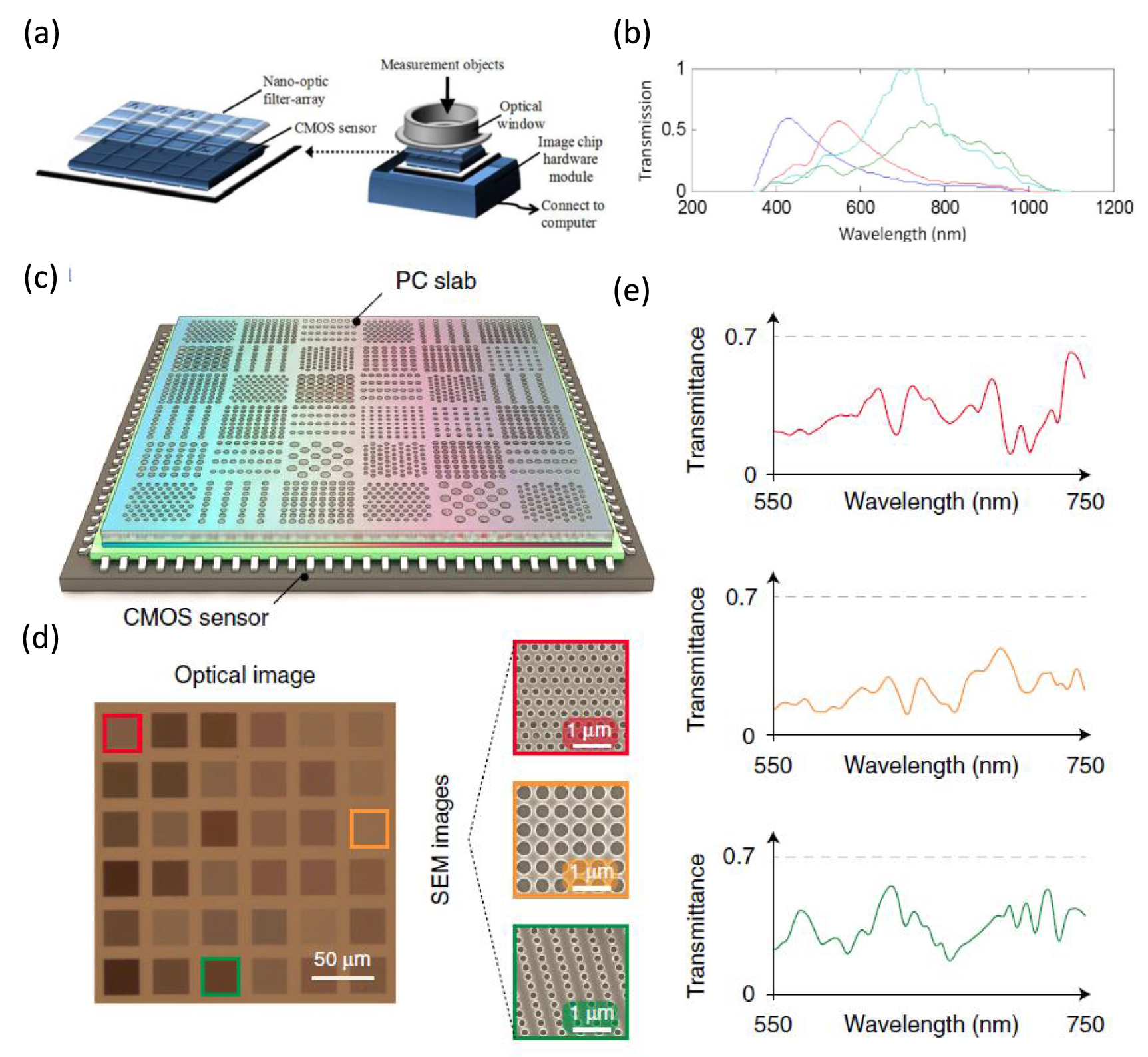
Figure 6. (a) Schematic of the low-cost nano-optic filter-based spectrum sensor used in this work for spectrum reconstruction and (b) transmission functions of four of the 195 nano-optic filters. Micro-spectrometer based on PC slabs. (c) Schematic of the spectrometer, which consists of an array of PC slabs with different parameters. These slabs are integrated on top of a CMOS sensor array. (d) Optical image of the fabricated 6 × 6 PC structures. Three SEM images of selected PC-slab structures marked by red, orange, and green frames, respectively, are shown on the side. (e) Measured transmission spectra T(λ) of the three structures in (d). For each PC slab, the corresponding T(λ) is characterized using a monochromater [14, 20].
Download figure:
Standard image High-resolution image
Figure 7. (a) Real-color PL image of a typical bandgap-graded CdSx Se1−x nanowire and corresponding spectra collected from the marked representative regions (spot size 5 μm). Scale bar is 20 μm. (b) A typical nanowire spectrometer in the form of a packaged chip. (c) Sensitivity of nanowire photo-detectors. Low-frequency noise density spectra of typical photodiode and photo-conducting detector (photoconductor) under different bias conditions. The instrumental background is also shown. (d) Schematic and image of the end-to-end configuration for on-chip PL measurement. (e) Schematic illustration of silicon nanowire microspectrometer, comprising 24 pixels arranged in a circular pattern. (f) Schematic illustration (cross sectional view) of a single pixel [21, 34, 35].
Download figure:
Standard image High-resolution image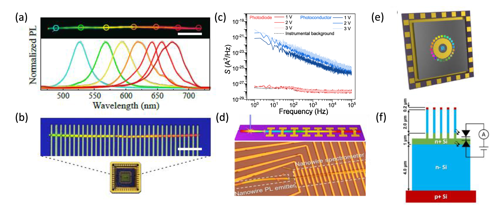
Accurate spectrum reconstruction was realized by regularization techniques and constrained optimization method shall be applied [79]. The method of Tikhonov regularization and with the L-curve method for parameter selection for stabilizing the solution of inverse problems is applied to the prototype nano-optic filter-based spectrum sensor for spectrum reconstruction, which was found useful to deliver satisfactory estimate. NanoLambda has been developing a chip scale spectrum sensor based on the new plasmonic filter array technology as well as this spectrum reconstruction method.
3.1.2. Photonic-crystal slabs miniature spectrometer
A photonic bandgap fiber bundle spectrometer is realized in 2010 with very limited R of 30 nm. Unlike the regular bandgap dispersion, series of broad irregular but coded transmission spectra could be used for spectra reconstruction, which benefits from wavelength multiplexing and advanced spectra reconstruction algorithm, meanwhile overcomes the limitation like the FTIR spectrometers need regular sine or cosine modulation to obtain interferogram for spectra retrievement. A single-shot spectral imaging method was proposed by Yu et al by using complex optical interference in PC slabs array as the dispersive filter [20, 80], which are micrometer-thin dielectric layers with periodic patterning. Light incident from free-space can couple to lateral propagation modes, where the periodic nanostructures allow light to bounce back and forth many times. Unlike microcavities, where the path enhancement only occurs at resonant frequencies, the effect of path enhancement in PC slabs spreads over a broader spectral range and creates a transmission spectrum with rich spectral features, including sharp peaks due to guided resonances, broad background variation by Fabry–Perot resonance, and irregular line shapes due to Fano interference. To work as a spectrometer, arrays of different PC slabs are fabricated on top of a CMOS imaging sensor. Each PC slab has a different periodicity, lattice constant, and hole sizes. These slabs creates a transmission spectrum with unique and rich spectral features. The authors recovered broadband spectrum from 550 to 750 nm with spectral resolution of ∼1.5 nm by regularization method. The spectrometer is CMOS compatible and promising application for lab-on-a-chip and hyperspectral imaging. However, the transmission through PC slabs is angle dependent, thus the spectrometer requires the incidence angle to be the same for the calibration and measurement, the performance degrades if the two angles are different by more than 1 degree, in practical application, it requires a collimating aperture to ensure a consistent incident angle. Alternatively, the PC slabs offer a flexibility to reduce the size of PC slabs to increase the angle tolerance at the cost of poorer spectral resolution.
3.1.3. Single bandgap-gradient CdSxSe1−x nanowire spectrometer
A monolithic single nanowire miniature spectrometer was realized by Hasan [34] and Wang [35], taking fully advantages of bandgap-graded semiconductor NW. Firstly, bandgap-graded semiconductor nanowire is a promising wavelength selective component for the advanced on-chip spectrometer because of its large and continuously tunable absorption range (from 505 to 710 nm). Secondly, the nanowire naturally supports fabricating linear array photo-detectors in a facile way and has a miniature footprint. The composition-graded CdSx Se1−x single nanowires which were first fabricated by Tong and Yang in Zhejiang University [81], are synthesized by vapor–liquid–solid method in a horizontal quartz tube mounted in a furnace using a source moving thermal evaporation technique. Figure 7(a) shows the fluorescent photo of a typical nanowire. The gradually changed luminescence color already implies a changing of bandgap.
Using these wires, Hasan et al fabricated conductive photodetectors array along the nanowire as shown in figure 7(b). By using this nanowire miniature spectrometer, they realized spectra reconstruction with R of 5 nm (with 38 devices, the more the devices the finer of the R), the BW is determined by the bandgap of the NW. They also demonstrated the capacity of spectral imaging from centimeter-scale focal planes down to lensless, single-cell-scale in situ mapping. Furthermore, Wang fabricated Schottky diode as photodetector array along the NW, instead of photoconductors, and demonstrate its very promising application in on-chip measurement. Comparing the Ohmic photo-conducting detectors, the Schottky diode has very low dark current, faster response time and, the most importantly, has very low figure of noise, and thus higher sensitivity larger than 1013 Jones which is almost two orders higher than its photoconductor counterpart given in figure 7(c). For the on-chip luminescence measurement, spectrometers with higher sensitivity is highly demanded for weak light detection. Another advantage is that nanowire also support waveguide-mode operation, in this way, it naturally allows detecting spot light source emitted from single quantum dot or molecule; as well as the waveguide mode can also enhance the light–matter interaction during light propagation along the guiding and active nanowire. And it does not change the photo-response dispersion as that operated in far-field mode.
Equipped with this high sensitivity nanowire monolithic spectrometer, on-chip PL measurement was carried out by aligning other long nanowires with the nanowire spectrometer in end-to-end configuration (figure 7(d)). Positioning an excitation laser at the far-end of emission nanowire, PL emits out from the near-end can directly enter the spectrometer by face-to-face coupling. And the spectrometer is operated in the waveguide mode, which allows all the photodiodes to simultaneously obtain photocurrent. Figure 14 shows the PL (at a power lower than 0.1 pW) and retrieved spectra. The reconstruction accuracy obviously relays on the sensitivity of the sensors, highlighting the importance of light–matter interaction in microspectrometer. For the commercial application, this strategy still needs well developed nanowire assembling technique for CMOS compatibility.
3.1.4. Detector-only miniature spectrometer
As we know silicon photodiode is a good detector for visible light. Vertical silicon nanowire (Si NW) array can act as filter due to its cavity effect, tunable absorption spectra can be achieved by tuning the radius of NW array [36]. Thus recently, Crosier et al employed Si NW photodetector array only as a miniature spectrometer [21, 82], on the one hand, the NW array act as filters for the effect of waveguide enhancing the resonant wavelength absorption, on the other hand, each Si NW is a photodetector which converts light to current recorded by the outer circuit. Given the absorption spectrum of each array and the output photocurrent signals, combining with the reconstruction method, the spectrum of the incident light can be retrieved. This spectrometer consists of 24 pixels of Si NW array that vary in radius from 60 to 175 nm, with height around 2.8 μm, each NW pixel has an extent of ∼150 μm × 150 μm. It demonstrates R with 5–6 nm and cover from 400 to 800 nm, practical measurement should make a trade-off between R and BW due to limited pixels. The paradigm of detector-only spectrometer of combining the detector and filter in one is a breakthrough in this area, but the complex fabrication process and reliability will be a challenge for practical application, especially the slow EBL writing process will limit its performance and device output.
A summary of the main bandgap dispersive micro spectrometers is presented in table 3.
Table 3. A summary of the broadband dispersive microspectrometers with key performance metrics.
| Configuration | Device footprint | Bandwidth | Resolution | Detector/Sensitivity related | CMOS compatible | Ref. |
|---|---|---|---|---|---|---|
| Nano-Optic filter | ∼mm2 | 350–1050 nm | 10 nm | Detector array | YES | 14 |
| Tunable Plasmonic filter | ∼mm2 | 480–570 nm | 1 nm | Detector array | YES | [76] |
| PC slab | 210 × 210 μm2 | 200 nm | 1.4 nm | Detector array | YES | [20] |
| CdSx Se1−x NW photoconductor | ∼100 μm | ∼500–750 nm | 5 nm | Self detection | YES | [34] |
| CdSx Se1−x NW photodiode | ∼100 μm | ∼500–750 nm | 5 nm | Self detection/1013 Jones | YES | [35] |
| Si NW | ∼cm2 | 300–700 nm | 5 nm | Self detection | YES | [21] |
'+' means additional requirement for integration.
4. Applications and conclusions
The selected examples that we have presented in the review show the remarkable paradigms for miniature spectrometer which also have great potential application outside laboratory for material and chemical analysis, such as portable devices and smartphone based chemical analysis. At present, a trade-off could be made among the metrics according to the requirement in different application situation. For the submarine where in situ analyze rare plants or animals by analyzing the fluorescence spectrum or space exploration laboratory where analyze spectrum to find new stars or determine the age of the celestial body, a portable compact spectrometer with satisfying resolution is space saving and versatile to do on-site measurement. For the application in microbiology, chemical analysis, food monitoring and gas sensing where optical spectrum with fine structure should be identified, resolution is more important than other factors. By leveraging advances in semiconductor microfabrication technologies, chip-integrated PL and Raman measurement and biosensors are poised to make an impact as scalable measurement tools for lab-on-a-chip applications where the miniature spectrometers with high sensitivity as well as low-cost are greatly demanding. The size of spectrometer has clearly gone through a period of rapid shrinkage with fine resolution and broad operation spectral range over the past decades. But rare work focus on the sensitivity, challenges come from inevitable small volume of incident light due to scaling down. Further work could take advantage of micro- and nano-photonics technologies such as polariton, evanescent near field to enhance the light–matter interaction to improve its sensitivity. The realization of scalable on-chip spectrometer with high performance is a systematic work including improving the performance of every key optical components such as detectors (sensitivity and spectra range), light splitter (discussed in the review), low loss light propagation components such as waveguide, interferometer and the light couplers. Efforts are still needed to explore new materials, new device structure and new mechanism to improve the performance of miniature spectrometer for a lab on-a-chip functionality.
In conclusion, miniature spectrometers with high performance will find a vast field of applications: research to commercial, industries to civilian, space to ocean, wearable to implantable, to name a lot. As the spectrometer has at least two parts: light splitting and detecting components, efforts for miniaturization should be made on these two parts. Among these spectrometers in this review, combining splitting and detection functionalities in one nanowire is really an inspiring and promising paradigm. As well as the nanowire spectrometer has an exciting potential application for hyperspectral imaging.
Acknowledgments
This project was primarily supported by the National Key R&G Program of China (Grant Nos. 2018YFA0307300, 2016YFA0200200 and 2018YFA0209100), the National Natural Science Foundation of China (Grant Nos. 61775092, 61934004, 61974064, 61874094 and 61674127), and the Collaborative Innovation Center of Advanced Microstructures. Strategic Priority Research Program of the Chinese Academy of Sciences (Grant No. XDB30000000) Program for high-level Enterpreneurial and Innovative Talent Introduction, Jiangsu Province.