

Abstract
We demonstrate a new technique for filling mm-scale microfabricated silicon and glass cavities with alkali vapors at the wafer-scale. A single etched silicon wafer contains an array of cavities containing alkali precursor materials offset laterally from the cell array. The wafer is heated to create an array of alkali droplets on an upper glass wafer, which is then translated laterally under vacuum and bonded to create the cells. This technique can be implemented in a commercially available bonding tool, allows the fabrication of cells with arbitrary buffer gas contents and pressures and can potentially produce cells with dimensions below 100 µm.
Export citation and abstract BibTeX RIS

Original content from this work may be used under the terms of the Creative Commons Attribution 4.0 license. Any further distribution of this work must maintain attribution to the author(s) and the title of the work, journal citation and DOI.
1. Introduction
Alkali vapor cells are important building blocks for microwave and optical frequency references [1], as as well as for precision magnetic [2, 3] and electric field [4] measurement instruments and other novel devices [5]. Fabricating these vapor cells is typically a complex and costly procedure because pure alkali metal, which is highly reactive with oxygen and water and readily consumed by glass at elevated temperatures, must be produced and distilled in an inert environment. Early demonstrations of microfabricated vapor cells used either direct deposition of alkali metal with a pipette [6] or in-situ [7] or ex-situ [8] chemical reactions. A review of approaches to the fabrication of alkali vapor cells using micromachining techniques can be found in [9].
The parallel fabrication of alkali vapor cells, in which an entire wafer of cells is fabricated using a single process sequence, has only been partially realized and existing methods have significant limitations. For example, alkali metal can be generated in a cell through UV-dissociation of RbN3 deposited into a cell cavity before bonding [7, 10]. However, the relative abundance of Rb and N2 is determined by the stoichiometry of the reaction, and only a few µg of Rb metal can be created in cells of volume 1 mm3, and N2 must necessarily be present. This precludes the fabrication of cells without buffer gases, which are needed for optical or Rydberg spectroscopy. A second wafer-level process is based on the dissociation of Rb2CrO4/Zr/Al in pill form which is thermally activated with a laser post-bonding [11, 12]. In this case N2 is gettered by the Zr/Al, making it challenging to include this buffer gas in the cell. Recently, it has been reported that some N2 can remain in the cell after activation [5]. This technique has been used successfully with a non-evaporable getter to produce a Rb vapor cell suitable for a high-performance, 2-photon optical clock [13]. In both cases, the post-activation is done cell by cell with a laser and residual chemical precursors remain in the cell, which can cause changes in the gas pressure over time [8] and obscure optical access. Often, a second cavity is needed separated by the vapor cell by thin channels to prevent the precursors or residual reactants from obscuring the windows of the cell cavity after activation.
In this letter, we demonstrate a novel method for fabricating alkali vapor cells in which the precursors are placed in an array of entirely separate filling chambers offset from the cell array by sim 1 mm. By heating the entire wafer under vacuum, Rb metal can be condensed into droplets on a glass surface placed over the cell array. The glass can then be translated laterally before bonding to move the alkali material into the cell cavities while leaving activated reactant residue behind in the 'deposition chambers'. The technique overcomes many limits imposed by alternative techniques. It allows for cells to be created with arbitrary buffer gases (or no gas at all); is compatible with whole wafers; potentially allows for very small cells with dimensions considerably below 1 mm; avoids reactant contamination; can incorporate isotopically enriched alkali metal; and uses a commercial anodic bonding tool, obviating the need for a custom vacuum system.
Historically, one of the first techniques used to microfabricate vapor cells employed a glass ampule situated above the cell to emit a beam of alkali metal into a cell cavity preform before bonding. The production of alkali metal was achieved using the substitution reaction BaN6+2RbCl  BaCl2+3 N2+2Rb [14] and enabled the separation of the reactants from the products. This proved important due to the observation of large drifts in vapor cells that retained both the reactants and products in the same chamber [8].
We adapt this technique to the wafer-scale by designing microstructures which incorporate the function of the alkali beam source into the wafer itself. This alleviates the complexity associated with having a retractable alkali beam source and permits arrayed fabrication using a single silicon wafer that contains both deposition cavities containing the reactants and the final cells themselves.
2. Experiment
We start with a silicon wafer 1 mm thick and 4 inches in diameter polished on both sides. In this wafer, we etch two arrays of holes using deep reactive ion etching, spaced by pitch 6 mm, and offset laterally from each other by 3 mm (see figure 1(a)). The holes on one array, which we term the 'deposition cavities', are square with dimension 0.75 mm and are designed to hold the chemical precursors. The holes in the second array, which we term the 'optical cavities', are also square but with dimension 1 mm, and will ultimately form the final cells. The 'unit cell' of this wafer is therefore composed of two cavities.
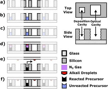
Figure 1. Right: Overview of the silicon geometry. Left: Overview of process. (a) Begin with a microstructured wafer of silicon replete with an array of pairs of holes (termed a 'preform wafer'). The small hole will form a 'Deposition Cavity' and the large hole will an 'Optical Cavity'. (b) Fill the deposition cavities with an aqueous mixture of RbCl+BaN6; allow to dry. (c) Place the preform wafer in a vacuum chamber and pump down with a glass wafer held above the preform wafer. (d) Heat the wafer stack; allow the precursors to react and observe the formation of alkali droplets on the uppermost window surface due to an induced thermal gradient. (e) Allow to cool; lift the glass wafer away allowing N2 gas to escape and translate the alkali droplets above the optical cavity. (f) Anodically bond the wafer stack shut at reduced temperatures. Upper right: depiction of the pair of cavities one termed the 'Deposition Cavity' which contains the initial reactants and a larger, adjacent cavity termed the 'Optical Cavity' which is to contain the alkali metal droplets isolated from the Deposition Cavity.
Download figure:
Standard image High-resolution imageThe silicon wafer is bonded to a standard borosilicate wafer (500 µm thickness) resulting in a 'preform wafer' with open holes on one side. The deposition cavities of this preform wafer are then filled with an aqueous solution of BaN6+RbCl using an automated pipetting system. The wafer is heated to 85 °C for 1 h to evaporate the water and leave a dried residue. This filled preform wafer is then inserted into an anodic bonding machine along with a second, standard borosilicate wafer (500 µm thickness) and placed under vacuum. The anodic bonding machine (AML AWB-04; Disclaimer: Certain commercial equipment is identified in this paper to foster understanding. Such identification does not imply recommendation or endorsement by the National Institute of Standards and Technology, nor does it imply that the materials or equipment identified are the best available for the purpose) is designed to allow the wafers to be moved with respect to one another under vacuum for alignment purposes. The two wafers are then brought into contact and the lower wafer is heated causing the precursors to react and evolve Rb and N2 gas. Due to the thermal gradient from the asymmetric heating profile, Rb droplets condense onto the lower surface of the upper glass wafer. The wafers are then passively cooled (typically overnight), decreasing the vapor pressure of the Rb and then pulled apart, releasing the N2 gas and allowing a second gas to be introduced if desired. The glass wafer with Rb droplets is then translated laterally and the droplets are positioned over the optical cavity. The two wafers are pushed together into contact and now the upper wafer is heated to 200 °C to enable a low-temperature anodic bond that takes place over 5 h. The thermal gradient is reversed and the Rb droplets are driven to the relatively cold preform wafer where they are not in contact with the hot glass surface to be bonded. A complete overview of this process is depicted in figure 1 on the left.
Two wafers were fabricated, one intended to contain evacuated cells with no residual gas, and the other where buffer gas is intentionally introduced at a known pressure into the chamber before the final anodic bonding step. After fabrication, optical spectroscopy on each cell on both wafers was performed at an elevated temperature with a laser, which we scanned across the Rb D2 line. The temperature of the buffer-absent cells was of 67 °C and the temperature of the buffer-present cells was increased to of 90 °C due to the decreased absorbance. From these measurements an estimate of the broadening and shift of the optical resonances with respect to a reference evacuated Rb cell can be extracted and hence establish the amount of residual gas density in each cell on the wafer.
For the evacuated cells, 125 deposition cavities were filled with chemical precursors and 35 of the final cells demonstrated clear Rb absorption signatures for a yield of 28%. Figure 2(a) depicts the normalized logarithm of the absorption for all microfabricated cells compared to a standard reference cell (indicated in green). We assume the dominant residual gas is N2 and use standard pressure broadening coefficients [15] to estimate the residual buffer gas pressure in each cell. A histogram of these pressures is shown in figure 2(b).

Figure 2. Experimental spectra and estimated residual background pressure. (a) Logarithm of the normalized absorption of the 35 successful cells across the wafer where the frequency axis is calibrated with a reference cell. The reference cell is measured in a typical saturated absorption spectroscopy configuration. A distribution of linewidths and center shifts is observed indicating some residual buffer gas contribution. Note the two cells with excessive pressure broadening. (b) Histogram of calculated residual buffer gas densities assuming N2 to be the dominant contaminant.
Download figure:
Standard image High-resolution imageMost cells show some residual gas. This can be partially attributed to the method of cleaning the wafers after filling with the aqueous solution. As the solution dries, it may precipitate proud of the surface of the preform wafer and prevent clean anodic bonding. This precipitate was cleaned but flakes were distributed into some of the optical cavities. While N2 drying was applied to flush the flakes out of the preform, some flakes were likely left behind. These flakes are able to evolve N2 when heated and may describe the variation in residual pressures in some of the cells see in figure 2.
The cell with the lowest residual pressure was measured using saturated absorption spectroscopy (SAS) as a fine measure of residual gas content. One trace of this spectroscopy is depicted in figure 3. The linewidth was measured as a function of optical power to extract the zero-power linewidth, which was measured to be 20.5 MHz and includes broadening due to residual gases, the magnetic field gradient from the heater, the DBR linewidth (≈1 MHz), Rb-Rb collisions (<100 kHz at an operating temperature of 67 °C), and angular mismatch of the pump/probe beams (≈650 kHz). Subtracting the known confounding variables yields 14.5 MHz of broadening due to the combination of the magnetic field gradient and the residual pressure. Neglecting the magnetic field gradient, the estimated residual pressure is ≈0.1 kPa of N2 gas at room temperature. The shift of the absorption spectrum was measured with respect to that of a reference cell to be less than 2.5 MHz implying a residual pressure of ≈0.06 kPa.
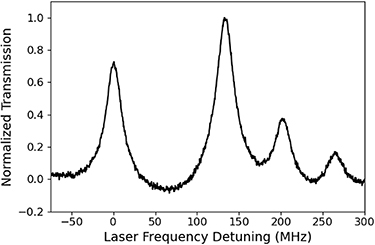
Figure 3. Optical spectroscopy of the lowest residual pressure vapor cell fabricated so far. Due to power broadening, the intrinsic linewidth of a hyperfine resonance is narrower than was measured here; the zero-power linewidth is estimated to be than 20.5 MHz implying approximately 14.5 MHz of broadening. The clear observation of hyperfine spectra indicates the low residual pressure in this vapor cell. This spectra has a quadratic function subtracted to approximate removal of the background Doppler-broadened profile.
Download figure:
Standard image High-resolution imageThe optical density also shows a distribution due to the impact of the buffer gas collisions on the atomic absorption cross section. However, due to variable beam clipping and the variable impact of optical pumping in each cell depending on the pressure, the extraction of the buffer gas pressure using optical density measurements contains greater uncertainty than the prior analysis.
This best cell indicates that sub-kPa residual pressures are achievable and further process refinements can reduce the distribution of residual pressures in these cells.
The intentional addition of a buffer gas at the few tens of kPa level reduces wall relaxation, enables efficient optical pumping and reduces Doppler broadening of microwave transitions of atoms in the cell. A buffer gas is therefore a desirable feature of CPT atomic clocks and magnetometers.
A wafer of buffer gas cells was fabricated as follows. After the Rb droplets are deposited on the upper glass wafer surface and the wafer stack is allowed to cool (step d in figure 1), the wafers are lifted apart and any residual N2 gas evolved during the reaction is pumped away. After cooling to room temperature, the bonding chamber is backfilled with N2 at a pressure of 28 ± 1 kPa at a temperature of approximately 35 °C, measured after a gate valve connecting the chamber to the vacuum pumps is closed. This corresponds to approximately 11.2 mol m−3 (0.25 amg) of N2 gas within the chamber. The wafers are pressed together and then bonded at a temperature of 200 °C. In this case, the wafer was patterned with 499 cavity pairs, of which 350 were filled with precursors. After bonding, Rb absorption was observed in 109 optical cavities for a yield of 31%.
The optical spectra of the cells in the second wafer are shown in 4(a). We simplify the hyperfine structure by approximating the manifold as a single resonance positioned in the center of mass of the hyperfine spectrum. The logarithm of the normalized transmission spectrum is taken and the resulting lineshape is fit to a sum of four Lorentzians with fixed relative amplitudes and center separations but variable linewidths corresponding to the 85Rb Fg
= 1  F
F = (0,1,2), 85Rb Fg
= 2
= (0,1,2), 85Rb Fg
= 2  Fe
= (1,2,3), 87Rb Fg
= 2
Fe
= (1,2,3), 87Rb Fg
= 2  Fe
= (1,2,3), and 87Rb Fg
= 3
Fe
= (1,2,3), and 87Rb Fg
= 3  Fe
= (2,3,4) resonances present in the D2 absorption spectrum. Because the buffer gas linewidth broadening is an order of magnitude greater than the Doppler-broadening, we neglect the Doppler broadening. The resulting Lorentzian linewidths are then used as a measure of the optical broadening due to the applied buffer gas density [16] and these linewidths are divided by 19.2 GHz amg−1 to convert the homogeneous broadening into a buffer gas density estimate. The results of this fit are displayed in figure 4.
Fe
= (2,3,4) resonances present in the D2 absorption spectrum. Because the buffer gas linewidth broadening is an order of magnitude greater than the Doppler-broadening, we neglect the Doppler broadening. The resulting Lorentzian linewidths are then used as a measure of the optical broadening due to the applied buffer gas density [16] and these linewidths are divided by 19.2 GHz amg−1 to convert the homogeneous broadening into a buffer gas density estimate. The results of this fit are displayed in figure 4.

Figure 4. (a) Experimental spectra measured at a temperature of 90 °C and fit with 4 pinned Lorentzians. (b) Histogram of calculated equivalent density distribution of buffer gas filled cells through linewidth conversion.
Download figure:
Standard image High-resolution imageThe results of this analysis result in a distribution of buffer gas pressures with a mean of 10.8 mol m−3 with a 1σ standard deviation of 1.1 mol m−3. The mean estimated density in these vapor cells 10.8 ± 1.1 mol m−3 is consistent with the estimated density added 11.0 ± 1.1 mol m−3). A photograph of a completed wafer is shown in figure 5 with a typical cell shown inset. This photograph shows the ability to produce macroscopic quantities of alkali metal with a hermetic anodic bond with high uniformity.

Figure 5. Photograph of a completed wafer of vapor cells. This wafer shows excellent bonding aside from some delamination in the upper left of the wafer. Inset: zoom of a single vapor cell demonstrating good bonding and no presence of fringes (fringes would indicate a bond void) and this cell contains a macroscopic volume of Rb metal. Modifications of the process recipe can result in less (or more) Rb deposited in each chamber and the excess Rb here is a notable advance over methods that employ RbN3 decomposition which limits the total volume of Rb metal by the fixed ratio of evolved N2 gas.
Download figure:
Standard image High-resolution image
3. Discussion
The process described here has several important advantages compared to existing methods of fabricating alkali vapor cells. First, it is a wafer-level process allowing many cells to be fabricated with a single process sequence. It uses commercially available bonding equipment, removing the need for designing a custom vacuum apparatus. Since the reactants other than the alkali metal remain in the deposition chambers, the cells contain few impurities which can cause long-term drifts in the buffer gas pressure and corresponding frequency drifts in atomic clocks [8]. Furthermore, the ability to decouple the volume of alkali metal produced from the final buffer gas pressure allow for arbitrary quantities of alkali metal to be contained in the cells as well as arbitrary buffer gas compositions and pressures limited only by buffer gases that would impede anodic bonding. By using microfabricated alkali effusion cells to deposit the alkali metal into the optical cavity, we achieve higher spatial localization of the metal than typically achieved through usual micropipetting. As a result, it may be possible to fabricate alkali vapor cells with dimensions well below 1 mm, and possibly as small as 50 µm. Such cells would further enable the integration of photonic devices with atomic vapors [17]. Small dimension cells also offer reductions in operational power and may enable new applications heretofore not realized.
4. Conclusion
In summary, we demonstrate a novel technique to produce alkali vapor cells at the wafer-scale using microfabricated alkali effusion cells integrated directly into the same wafer that forms the alkali optical cavities. We demonstrate clean, macroscopic quantities of rubidium with no residual precursor in the optical cavity in an anodically bonded package. We also demonstrate the mass fabrication of buffer gas alkali vapor cells with a narrow distribution of buffer gas pressures suitable for optical magnetometers. The capability to backfill with arbitrary buffer gas pressures and species overcomes the limitations of alternative wafer-level alkali vapor cell fabrication techniques.
Author's contributions
DGB and VMM contributed equally to this work.
Data availability
The data that support the findings of this study are available from the corresponding author upon reasonable request.
Acknowledgments
This work was performed at the National Institute of Standards and Technology using internal funding. Thanks to Jennifer Black and Matthew Simmons for helpful comments on the manuscript. Thanks to Susan Schima for processing expertise and time.