

Abstract
We report the effect of bias stress on the drain current and threshold voltage of n-channel thin-film transistors based on solution processed In2O3 layers. Application of a positive gate bias for variable time-periods led to displacements of the transfer curves in the positive gate bias direction. On switching off the gate bias, the transfer curves returned close to their pre-stress state on a timescale similar to that when the gate bias was switched on. The time dependence of the threshold voltage shift is described well by a stretched-exponential model. The temporal behaviour of the threshold voltage shifts is consistent with charge trapping as the dominant effect, although some defect formation cannot be ruled out.
Export citation and abstract BibTeX RIS

Original content from this work may be used under the terms of the Creative Commons Attribution 4.0 license. Any further distribution of this work must maintain attribution to the author(s) and the title of the work, journal citation and DOI.
1. Introduction
In recent years, transparent oxide thin film transistors (TFTs) have been extensively studied due to their high-performance and potential use in various low-effective technological application [1–6]. Recent investigations demonstrated the key properties of oxide TFTs, including device mobility [6], film uniformity over large areas [7], high optical transparency in the visible region [8], low off-current and compatibility with various fabrication methods [9, 10]. The development of large-area, low cost devices relies strongly on the fabrication methods and the choice of materials [11, 12]. A number of metal-oxide based TFTs such as indium oxide (In2O3), indium zinc oxide (IZO), and indium gallium zinc oxide (IGZO) have demonstrated high mobilities and reasonable device performance at low or room temperature, using different device dimensions and various fabrication methods [13–16].
In2O3 is one of the most important and promising semiconductor materials for such applications due to its wide band gap, high symmetry cubic structure, phase purity and low cost [17]. In2O3 has been effectively prepared by various techniques, such as magnetron sputtering [18], electro-spinning [5, 19], atomic layer deposition [6, 20, 21] pulsed laser deposition [22, 23] and spray pyrolysis [7]. One of the key issues for In2O3 thin-film devices is the stability of the threshold voltage after prolonged application of gate voltage, referred to as bias stress [24, 25].
Due to the attractiveness of its use in recent electronic devices, it is crucial to understand the key mechanisms that influence the performance and stability of the solution-processed metal oxide TFTs. We report an experimental investigation of the effect of bias stress effect on top-contact bottom-gate In2O3 device stability over prolonged bias stress. Device recovery after stress release and possible mechanisms of bias stress and recovery are discussed in the context of our experimental data.
2. Experimental procedure
The In2O3 precursor solution was prepared by dissolving anhydrous indium nitrate [In (NO3)3] (99%, Indium Corporation) in deionized water at a concentration of 30 mg ml−1. The solution was stirred at room temperature for 60 min before use. For the fabrication of low-temperature aqueous-based In2O3 TFT, the semiconductor thin-film deposition was carried out by spin-casting the In2O3 precursor solution onto highly doped Si substrates having a 100 nm thermally grown SiO2 gate dielectric layer at 3000 rpm for 30 s under ambient conditions, followed by a post-deposition thermal anneal process for 30 min at 200 °C. Procedures used for preparing and characterizing the films are described in [7, 26].
40 nm-thick Al top source and drain electrodes were deposited through a shadow mask. The sample size was 2 cm × 2 cm, and each sample included 98 devices. Where required, samples were cleaved to access fewer devices for use in the atomic force microscope (AFM). Transistors were bonded with gold wire of diameter 0.06 mm with conductive silver paint (Silverdag, Agar Scientific) under an optical microscope. Devices having channels of varying length (L) and width (W) were prepared and stored under vacuum to prevent degradation. Device current–voltage (I–V) data were recorded with a Keithley Picoammeter-6487, controlled using a python script. Scanning probe microscopy images were performed using a Bruker Multimode instrument in intermittent contact mode.
3. Results and discussion
As-grown films are found to be highly transparent across the entire visible spectrum (i.e. 400–700 nm), with an average transmittance of more than 95% (substrate-corrected values). A sharp absorption characteristic was observed in the UVA region as expected from the wideband gap property of indium oxide owing to its electronic inter-band transition (figure S1, supplementary information (https://stacks.iop.org/JPMATER/4/015003/mmedia)). AFM measurements were performed in intermittent contact mode to examine the surface morphology, as shown in figures 1(a) and (b), giving a root-mean-square surface roughness (σrms).
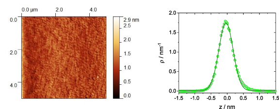
Figure 1. (a) AFM image of the 4 nm-thick indium oxide film in the region between transistor electrodes. (b) The corresponding height profile together with a fitted Gaussian curve. The root mean square (r.m.s.) surface roughness is 0.26 nm.
Download figure:
Standard image High-resolution imageIn terms of quantifying the performance of the transistor channel layer, the most important TFT property is its output and transfer characteristics. Figures 2(a) and (b) show a set of representative transfer and output characteristics of an In2O3 TFT of channel thickness 4 nm with channel width (W) and length (L) of 1000 μm and 30 μm, respectively. The source-to-drain current increase with increasing gate-source bias due to electron accumulation at the In2O3/SiO2 interface. The device shows excellent pinch-off characteristics, which indicates that electron transport in the channel is fully controlled by drain and gate bias. Furthermore, the device exhibits clear current–voltage modulation with drain current on-off ratio of nearly 105 and Vth = 2.1 V operating in accumulation mode in positive gate bias. The obtained saturation mobilities are in the range of 0.2–0.3 cm2 V−1 s−1 with n-type semiconductor behavior.

Figure 2. (a) The output characteristic for a In2O3 transistor (film thickness 4 nm, W = 1000 μm, L = 30 μm). The applied gate bias was incremented in 1 V steps from VG= 1 V to VG= 10 V. (b) The corresponding transfer characteristics at VD = 10 V. The resulting values for Vth and μsat are (2.07 ± 0.12) V and 0.22 cm2 V−1 s−1 respectively.
Download figure:
Standard image High-resolution imageThe electrical stability of TFTs is important for stable display performance. Bias stress instability leads to threshold voltage shift with time during application of gate voltage, which in turn causes a decrease in drain current. Therefore, the generation and recovery of these instabilities over time may lead to time-dependent operation of the device, followed eventually by dysfunction. Bias stress can potentially lead to instabilities such as charge trapping, defects in the active channel layer, in the gate dielectric, and at the active layer/dielectric interface. Mechanisms for such degradation have been proposed. For instance, Nomura et al [27] in the study of a-In-Ga-Zn-O suggested that shallow traps are the origin of large threshold voltage shift (∼10 V) and subthreshold deterioration observed in unannealed devices, while deep traps are responsible for small shifts (∼1 V), not removed by annealing. On the other hand, Lei et al (2008) and Suresh et al (2008) [25, 28] attributed degradation to charge trapping in the channel/dielectric interface and bulk semiconductor. Strategies to mitigate carrier trapping and reduce the associated bias-stress have also been reported [29].
With the source electrode grounded and the drain bias fixed at 10 V, the gate bias was applied for an extended period, with regular interruptions, each of 5 s, to record the transfer characteristics for a sweep of VG from −5 V to 16 V. The quoted stressing time is the cumulative time during which the bias stress was applied. Figure 3 shows a set of transfer curves of a TFT transistor having channel width and length of 1000 μm and 30 μm respectively. Transfer curves for different stressing times reveal progressive shifts toward larger threshold voltages. The positive shifts of threshold voltage with stress time could be due to electron trapping at the channel/dielectric interface or injected into the dielectric or creation of defect states at or close to the channel/insulator interface [24, 29–31].
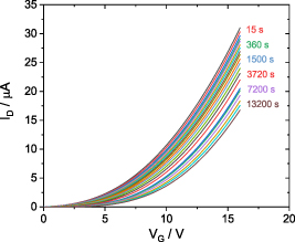
Figure 3. Transfer characteristic curves shift with stressing time of W = 1000 μm and L = 30 μm. The drain bias was 10 V and the stressing gate bias was maintained at 10 V for stress time durations of 0, 15, 30, 90, 150, 240, 360, 540, 780, 1080, 1500, 2100, 2820, 3720, 4920, 6720, 7200, 8400, 10 800, and 13 200 s.
Download figure:
Standard image High-resolution imageTrapped electrons at the interface between active layer and oxide dielectric reduce the effective gate bias and consequently shifts the threshold voltage in the positive direction. The lower effective gate bias results in smaller drain current flow through device channel, requiring increased gate bias to switch on the device and reach saturation [21]. The shift in threshold voltage as a function of time t is

It is well known for a TFT that there are two effects causing instability: defect creation in the channel and charge trapping in the dielectric material and at the channel/insulator interface [24]. Defect creation leads to lasting changes in the sub-threshold slope and device mobility, whereas charge trapping does not [32]. Figure 4 shows the variation of device mobility with stress time, which reveals a slight change in the device mobility over long stress periods.
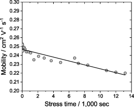
Figure 4. Variation of mobility with stress time (film thickness 4 nm, W = 1000 μm, L = 30 μm).
Download figure:
Standard image High-resolution imageCharge can be trapped either in the channel or at its interface with the dielectric or by injection into the dielectric. The major difference between charge trapping at the interface and injection into the dielectric is the amount of energy needed to remove the injected charge: higher energy is required to release charge injected into the dielectric, usually requiring thermal annealing or application of bias [33]. Our device dielectric material was 100 nm-thick thermally grown silicon dioxide which has a low density of bulk trap states so the fact that the device recovers quickly without annealing indicates that transient charge trapping or induced states are mainly involved.
The threshold voltage shift observed for our indium oxide TFTs can be well described as a function of time t with the stretched exponential equation [28, 34].

where ![$\Delta {V_{\mathrm{th}0}} = \left[ {{V_{\mathrm{th}}}\left( {{\text{t}} \to \infty } \right) - {V_{\mathrm{th}}}\left( {t = 0} \right){\text{ }}} \right].$](https://content.cld.iop.org/journals/2515-7639/4/1/015003/revision5/jpmaterabc608ieqn1.gif) Here,
Here,  is the stretched function exponent and τ represents the characteristic trapping time (time constant) which correlates with the average effective energy barrier. Equation (1) is an empirical function introduced by Rudolf Kohlrausch in 1854 to describe the time dependent discharge of a capacitor, sometimes known as the Kohlrauch function. The exponent
  describes the degree of deviation from an exponential function. When
  is close to unity, it indicates a narrow distribution of time constants, the limiting value of 1 corresponding to a single time constant. Smaller values of
  imply a broader distribution of time constants [35]. Figures 5(a) and (b) shows the fitting of threshold voltage shift with stressing time according to equation (1) on both a linear and a logarithmic scale.

Figure 5. Time dependence of the threshold voltage shift under an applied gate bias stress 10 V on a linear scale (left) and logarithmic scale (right). The green lines show the optimized fit of the Kohlrausch function (equation (1)) to the data, the resulting fitted parameters being ΔVtho = 1.86 ± 0.06 V, β = 0.53 ± 0.14, and τ = (3.64 ± 0.23) × 104 s.
Download figure:
Standard image High-resolution imageThe experimental data of the threshold voltage shift with stressing time agree well with the stretched exponential function presented in equation (2) and the extracted fitting parameters from curve fitting are ΔVth0 = 1.86 ± 0.06 V, β = 0.53 ± 0.14, and τ = (3.64 ± 0.23) × 104 s. Based on the gradual channel model and the stretched exponential function of  , the drain current can be written as [36].

Figure 6 shows the time-dependent drain current under positive stress. The reduction in current with stress time is clear with a fast initial decrease and a slow decrease at extended time without establishing a steady state. After the gate bias was switched off, the current recovery was rapid in the first few seconds but slows thereafter. The measured drain current under varied stressing time also agreed with equation (2), giving fitting parameters β = 0.52 ± 0.11, τ = (3.60 ± 0.16) × 104 s, consistent with those obtained from the fit to the threshold voltage shift. As noted, in common with many experimental studies of bias stress, the threshold voltage shift as a function of stressing time was monitored by regular transfer characteristics. Ideally, the bias stress should be applied without such interruptions in which VG is swept repeatedly. Each sweep of VG took 5 s, during which it is estimated that the threshold voltage shift reduced by ∼0.04 V, about 2% of ΔVth0 . The cumulative effect of such partial stress relaxations may influence the threshold voltage shifts recorded for extended stress times. The alternative approach of measuring each threshold voltage shift on a singly stressed new sample would considerably increase the experimental effort involved.
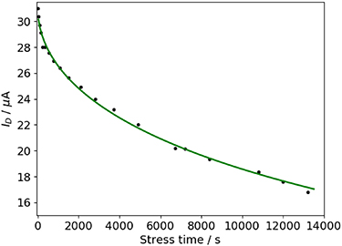
Figure 6. Drain current decrease with stress time according to equation (2). The extracted fitting parameters are Ido = 3.08 × 10⁻⁵ A, β = 0.52 ± 0.11, and τ = (3.6 ± 0.16) × 104 s.
Download figure:
Standard image High-resolution imageThe values of the time constant τ and the stretching parameter β obtained from these fits are similar to those reported for IGZO. For IGZO, reported values of τ are generally in the range 2000–20 000 s [28, 37–39] with occasional reports of values of the order of 105–106 s [40]. The reported values of β for these papers lie in the range 0.4–0.8. Multilayer hybrid In2O3/ZnO nanoparticle TFTs display strong stability to bias stress with a long time constant τ = 2.6 × 10⁸ s and β = 0.40 [41]. (For these multilayers, n-type doping of the Zn nanoparticles with aluminium reduces τ to 6000 s with β = 1.0 [41], likely related to the lineup of the dopant levels with the conduction band minimum.) Our fitted values indicate that the bias stress behaviour in solution-processed In2O3 films is similar to that observed in IGZO.
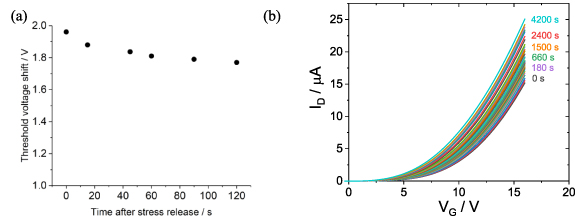
In some electronic applications such as active matrix displays, the TFT is switched on only for limited time, so the resulting shift in threshold voltage relaxes in the off state. Therefore, recovery is as important as stress and the device should return to its original state after stress release. The recovery of  after switching off the bias stress was monitored, and we found that the threshold voltage shift is almost fully reversible and recovered gradually, as seen in figure 7, with
  = 0.17 V after 4200 s, ∼10% of its value in the stressed state before relaxation. The drain current ID
after 4200 s is also slightly reduced compared to that at a corresponding VG in figure 3. This reversibility indicates that the stress is rapidly and almost fully released when the gate bias switched off.
= 0.17 V after 4200 s, ∼10% of its value in the stressed state before relaxation. The drain current ID
after 4200 s is also slightly reduced compared to that at a corresponding VG in figure 3. This reversibility indicates that the stress is rapidly and almost fully released when the gate bias switched off.
Figure 7. (a) Threshold voltage shift as a function of relaxation time immediately after stress release. The data indicate a threshold voltage shift of ∼0.04 V (∼2%) within the 5 s period for each sweep of VG in measuring regular transfer characteristics for figures 5 and 6. (b) Transfer characteristics back shift after stress release of device W= 1000 μm and L= 30 μm. The gate bias switched off and a rapid sweep of ID vs VG was performed for t = 0, 15, 45, 90, 180, 240, 300, 360, 420, 480, 600, 660, 720, 780, 840, 900, 960, 1080, 1140, 1200, 1320, 1500, 1620, 1800, 2100, 2400, 2760, 3000, 3300, 3600, 4200 s.
Download figure:
Standard image High-resolution image
Published studies of the effects of bias stress in In2O3 films do not report fitting with a stretched exponential function for direct numerical comparison with our results. Vygraneko et al [24] measured threshold voltage shifts in In2O3 transistors, deposited by reactive ion beam-assisted evaporation, after applying a gate bias of + 10 V for 600 s and after 6000 s—and again 300 s after switching off the gate bias. Their results show broadly similar behaviour to ours, also showing fast recovery without annealing. A puzzling difference is their observation of a slight decrease in the threshold voltage shift for long stress times (>3000 s) whereas our results show an asymptotic approach to a constant value. Lee et al [42] compared the electrical stability of solution-processed In2O3 devices maintained under vacuum with those maintained in air. Repeated measurements of transfer characteristics showed a slow decrease in mobility in air and a slight increase under vacuum. Larger threshold voltage shifts in air were interpreted by the authors as the result of electrostatic interactions between electrons and polar water molecules at grain boundaries in the nanocrystalline In2O3 films [42].
4. Summary and conclusions
We fabricated solution-processed indium oxide TFTs with a top-contact bottom-gate structure exhibiting n-channel accumulation during operation. The effect of bias-stress measurements on indium oxide based TFT were investigated to check the device stability under prolonged gate bias. Fitting of the stressing time dependence of the threshold voltage shift with a stretched exponential function yields similar values of τ and β to those reported for IGZO. The trapping time constant is widely distributed: during the early stages of bias stress, traps of small time constant are initially filled. As the stressing time increases, traps with increasingly higher time constant get filled. Accordingly, a mechanism of wide distribution of time constants should provide either a distribution of energy barriers between majority carriers and traps or both. The rate at which Vth shifts during gate bias stress decreases with time (figure 5), as is observed in metal oxide, organic and amorphous silicon TFTs [34–36, 43–45].
Following bias stress of 10 V applied for 13 200 s, once switched off the threshold shift decreases, reaching around 10% of the value in the stressed state after 4200 s, indicating rapid and relatively complete relaxation during this time period. It suggests that charge trapping is the dominant process rather than defect creation which is irreversible at room temperature, though some defect formation cannot be ruled out. The exact nature and location of charge trapping cannot be unambiguously determined. A recent study comparing devices operated in air and in vacuum has proposed electron binding to water molecules at nanocrystalline grain boundaries in the channel as an alternative trapping mechanism [42]. Thus, future studies should focus on addressing the impact of microstructure on bias-stress stability of the TFTs. A simple way forward would be to study the impact of annealing temperature on In2O3 TFT operation, while microstructural analysis of the channel layer via non-destructive techniques, such as x-ray diffraction, could enable a detailed structure-property relationship(s) to be established. There is no doubt that elucidating the key processes responsible for the observed bias-instability in many oxide TFTs could help scientists to develop new materials and/or mitigation strategies, thus further accelerating the incorporation of the technology in commercial products.
Acknowledgments
IA acknowledges Salahaddin University for ongoing support. TDA acknowledges the King Abdullah University of Science and Technology (KAUST) for financial support.
Supplementary Material
Supplementary material for this article is available online
Supplementary data (0.1 MB PDF)