Article

Voltage-Mode Multifunction Biquad Filter and Its Application as Fully-Uncoupled Quadrature Oscillator Based on Current-Feedback Operational Amplifiers

1
Department of Electronic Engineering, National Chin-Yi University of Technology, Taiping, Taichung 41170, Taiwan
2
Department of Electronic Engineering, Ming Chi University of Technology, New Taipei 24301, Taiwan
3
Department of Electrical Engineering, California State University Fullerton, Fullerton, CA 92831, USA
*
Author to whom correspondence should be addressed.
Sensors 2020, 20(22), 6681; https://doi.org/10.3390/s20226681
Submission received: 4 October 2020 / Revised: 21 November 2020 / Accepted: 21 November 2020 / Published: 22 November 2020
(This article belongs to the Section Electronic Sensors)

Abstract

:
This research introduces a new multifunction biquad filter based on voltage mode (VM) current-feedback operational amplifier (CFOA) and a fully uncoupled quadrature oscillator (QO) based on the proposed VM multifunction biquad filter. The proposed VM multifunction biquad filter has high impedance to the input voltage signal, and uses three CFOAs as active components, while using four resistors and two grounded capacitors as passive components. The VM CFOA-based multifunction biquad filter realizes band-reject, band-pass, and low-pass transfer functions at high-input impedance node simultaneously, which has the feature of easy cascading in VM operation without the need for additional voltage buffers. Additionally, the filter control factor parameter pole frequency (ωo) and quality factor (Q) of the proposed VM multifunction biquad filter can be independently set by varying different resistors. By slightly modifying the VM multifunction biquad filter topology, a VM fully-uncoupled QO is easily obtained. The difference from the previous VM CFOA-based multifunction biquad filter is that the proposed VM CFOA-based multifunction biquad filter can be independently controlled by the filter control factor parameters, ωo and Q. The proposed VM CFOA-based multifunction biquad filter can be transformed into a VM QO with fully-uncoupled adjustable of the oscillation condition and the oscillation frequency. The oscillation condition and the oscillation frequency can be fully-uncoupled and controlled by varying two sets of completely different resistors. The proposed VM fully-uncoupled QO solves the amplitude instability. The constant amplitude ratio of two quadrature sinusoidal waveforms can be realized when tuning FO. PSpice simulation and experimental results prove the performances of the proposed VM multifunction filter and VM fully-uncoupled QO. Simulation and experimental results confirm the theoretical analysis of the proposed circuits.

1. Introduction

Voltage-mode (VM) analog active filters and oscillators using different active components have received extensive attention. Some innovative approaches to realize VM biquad filters [1,2,3,4] and oscillators [5,6,7,8,9] can be found in the open study. Single-input three-output VM multifunction biquad filters, such as band-pass filter (BPF), low-pass filter (LPF), high-pass filter (HPF) or band-reject filter (BRF), are applied to the phase-locked loop, the high fidelity 3-way speaker, the touch-tone telephone tone decoder, and the phase sensitive detection (PSD) [8,9,10,11]. PSD is suitable for detecting and measuring low frequency electrical signal from the sensor [8,9]. The conceptual scheme of a dual PSD including a VM quadrature oscillator (QO), an auto-balancing bridge circuit, two multiplier circuits and two LPF circuits module is shown in Figure 1 [8,9,10]. VM QO can generate two sinusoidal wave output with a 90° phase difference and is the great significant part of a PSD [8,9]. Based on the dual PSD system, low-frequency QOs and filters research are required. The potential applications and advantages of using current-feedback operational amplifiers (CFOAs) to design VM biquads have attracted considerable attention in [12,13,14,15,16,17,18,19,20,21,22,23,24,25,26,27]. CFOA can be obtained by the cascade of a positive second-generation current conveyor and a voltage follower, so it can be implemented by the commercially integrated circuit (IC) namely Analog Device AD844AN [28,29]. The voltage on the non-inverting input port +IN of AD844AN is transferred to the inverting input port -IN, and the current flowing to the inverting port -IN is replicated to the port Tz. The voltage output port O follows the port Tz voltage. Compared with conventional operational amplifier (OP-AMP), AD844AN has the advantages of wider bandwidth and higher slew rate [28,29]. Therefore, for a specific purpose design, a dual PSD system, or a small number of circuits, using a commercially available ICs to design a VM biquad filters and QOs is better choice. According to the AD844AN datasheet [29], the rated temperature range of AD844AN is −40 °C to +85 °C, which is industrial temperature range, and the power supply range of AD844AN is ±4.5 V to ±18 V. Hence, when the circuits operate at different temperatures, the performances of the circuits will not have obvious fluctuations. Based on the above advantages, AD844AN has been widely used in the open literature [12,13,14,15,16,17,18,19,20,21,22,23,24,25,26,27,28,29,30,31,32].
As mentioned above, it is beneficial to use CFOA as an active component to implement a variety of high-input impedance VM multifunction biquads. The VM biquads, which has a high impedance for the input voltage signal, has aroused great interest because this biquads can be easily cascaded without any voltage buffer [21,22,23,24,25,26,27]. Singh and Senani [23] proposed a VM multifunction biquad HPF, LPF, and BPF transfer functions, but it employed four CFOAs and eight passive components. Horng and Lee [24] proposed a VM multifunction biquad HPF, LPF, and BPF transfer functions using three CFOAs and seven passive components, but it had the disadvantage of using three capacitors. Shan and Malik [25] proposed another VM multifunction biquad BRF, BPF, LPF, and HPF transfer functions using four CFOAs and six passive components, but it had the disadvantage of using four CFOAs. CFOA-based VM multifunction biquad HPF, LPF, and BPF has been proposed [26]. The transfer functions of the proposed filter use three CFOAs and four passive components, where one of the X terminals of the CFOA is connected to a grounded capacitor, which will lead to an improper transfer function and poor performance at high frequency. In 2019, a CFOA-based high-input impedance VM multifunction biquad has been proposed [27]. This circuit has important advantages, such as using only three CFOAs and realizing the transfer functions of BRF, BPF and LPF at the same time. In addition, the circuit also has the advantages of single input and three outputs, high-input impedance, and quadrature adjustable pole frequency (ωo) and quality factor (Q), and easily converted to VM QO. However, a further advantage cannot be achieved in [27], that is, the independent tunability of the filter control factor parameters ωo and Q. Although the topology of VM multifunction biquad [27] can be converted to VM QO, it cannot achieve a fully-uncoupled tuning methods, and cannot obtain the condition of oscillation (CO) and the frequency of oscillation (FO). Note that only when CO and FO are determined by two completely different sets of components, CO and FO are called completely decoupled [30].
This research proposes a new topology for the realization of an independently tunable VM multifunction biquad filter. The proposed topology uses three CFOAs as active components, while using four resistors and two grounded capacitors as passive components. The advantages of the proposed CFOA-based VM multifunction biquad filter are follows: (i) use only three CFOAs, (ii) use only two grounded capacitors, (iii) realize three standard filter transfer functions with one input and three outputs at the same time, (iv) high-input impedance, (v) the input parasitic resistances of the X ports of the CFOAs can be easily accommodated in an external resistors, (vi) independent control of the filter control factor parameters ωo and Q, and (vii) transformed into a VM QO with fully-uncoupled adjustable of CO and FO. Table 1 compares the proposed VM multifunction biquad filter with previously published researches [12,13,14,15,16,17,18,19,20,21,22,23,24,25,26,27]. It can be seen that the proposed VM multifunction biquad filter can simultaneously achieve all the above imported properties. Unlike the recently reported in [27], the attractive feature of the proposed VM multifunction biquad filter can be controlled independently of the control factor parameters ωo and Q, and transformed into a VM QO with fully-uncoupled adjustable of CO and FO. Furthermore, the proposed VM QO with fully-uncoupled is advantageous to achieve amplitude stability. Table 2 summarizes the performance of the filter and oscillator, and compares the specific characteristics of the study [27].
In this research, a new VM multifunction biquad filter with high-input impedance and a VM fully-uncoupled QO using the proposed VM multifunction biquad filter are presented. Compared with the previous research [27], the proposed VM multifunction biquad filter can overcome the independent control of the filter control factor parameters ωo and Q, and the proposed VM CFOA-based QO can also overcome the fully-uncoupled adjustability of CO and FO. The CFOA-based biquad filter and QO are suitable for PSD system based on the use of commercially available ICs. The filter control factor parameters ωo and Q are independently tuned and controlled. The QO control factor parameters CO and FO are fully-uncoupled tuning controlled. The effective frequency ranges of the bqiaud filter circuit is around 1 MHz, and the QO oscillation frequency varies from 8.16 to 628 kHz. Moreover, the proposed QO with fully-uncoupled is advantageous to achieve amplitude stabilization. The remaining sections of the research is structured as follows. Section 2 will introduce the characteristics and non-ideality of the VM CFOA-based multifunction biquadratic filter. Subsequently, based on the proposed VM CFOA-based multifunction filter, the VM fully-uncoupled QO is introduced. Section 3 verifies the proposed VM CFOA-based circuits and the theoretical comparison between experimental data and simulation data. Finally, Section 4 will summarize the research.

2. Proposed VM CFOA-Based Circuits

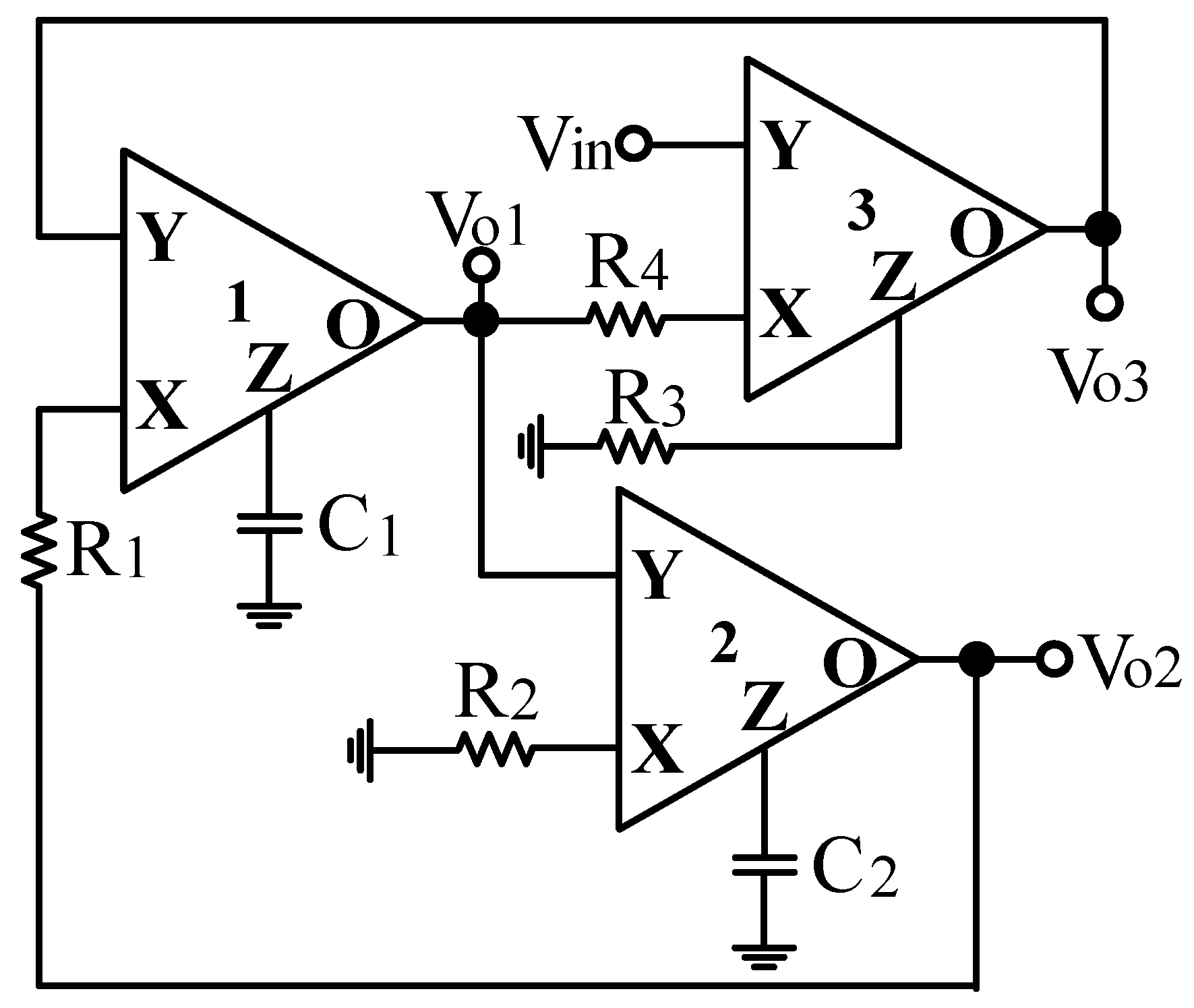
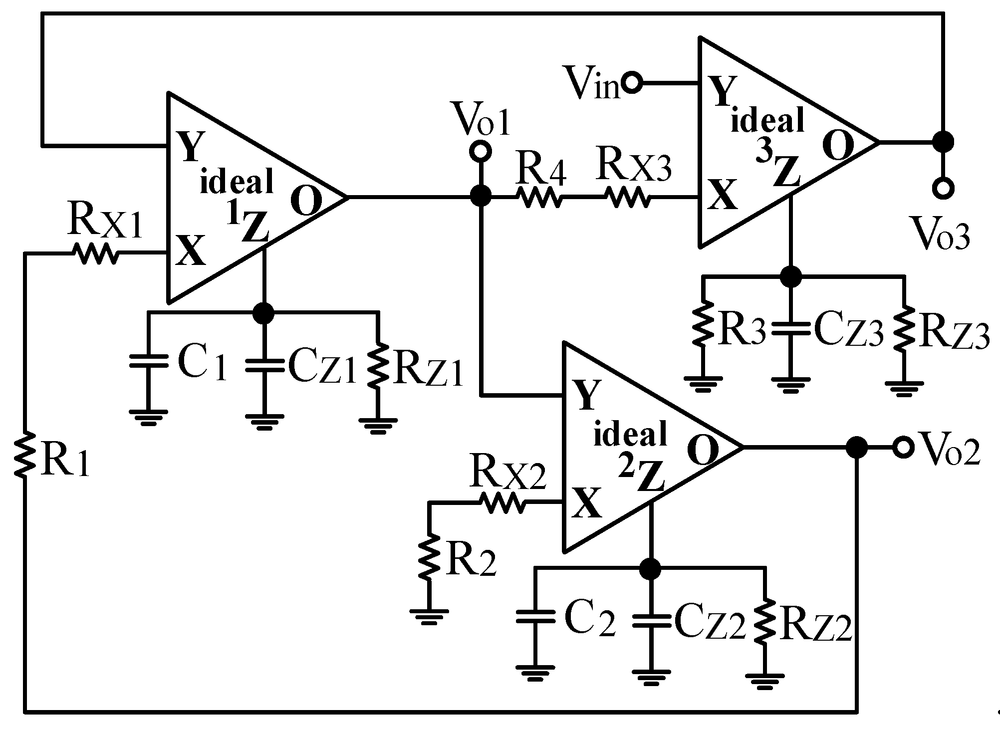
2.1. Proposed VM CFOA-Based Multifunction Biquad Filter

CFOA is a four-port versatile active component and its commercially available IC is AD844-type CFOA. The four-port characteristic of CFOA can be described by VX = VY, VO = VZ, IY = 0 and IX = IZ [31,32]. Figure 2 shows the proposed CFOA-based VM multifunction biquad filter with high-input impedance, including three CFOAs as active components, four resistors, and two grounded capacitors. Using only two grounded capacitors is particularly attractive for IC implementation. Routine analysis of the proposed filter yields the following BPF, LPF, and BRF voltage transfer functions.
V o 1 V in = s ( R 3 C 2 R 1 R 4 ) s 2 + s R 3 C 1 R 1 R 4 + 1 C 1 C 2 R 1 R 2
V o 2 V in = ( R 3 R 4 ) ( 1 C 1 C 2 R 1 R 2 ) s 2 + s R 3 C 1 R 1 R 4 + 1 C 1 C 2 R 1 R 2
V o 3 V in = ( R 3 R 4 ) ( s 2 + 1 C 1 C 2 R 1 R 2 ) s 2 + s R 3 C 1 R 1 R 4 + 1 C 1 C 2 R 1 R 2
As shown in Equations (1) to (3), the biquadratic BPF transfer function is obtained from Vo1, the biquadratic LPF transfer function is obtained from Vo2, and the biquadratic BRF transfer function is obtained from Vo3. The pass-band gain of the biquadratic BPF transfer function is unity. The pass-band gains, GLP and GBR, of biquadratic LPF and BRF transfer functions are given by
G LP = G BR = R 3 R 4
According to the denominator polynomial of the transfer functions of the CFOA-based VM multifunction biquad filter given in Equations (1) to (3), the filter control factor parameters Q and ωo of the filter can be calculated as
Q = R 4 R 3 C 1 R 1 C 2 R 2 ,   ω o = 1 C 1 C 2 R 1 R 2
Based on Equation (5), the following techniques for obtaining independent control of Q and ωo can be suggested. By changing R3 and/or R4, the control factor parameter Q can be independently controlled without disturbing ωo. For fixed-value capacitors, by simultaneously changing R1 and R2 while keeping the ratio of R1 and R2 constant, the control factor parameter ωo can be independently controlled without disturbing Q. Thus, the CFOA-based VM multifunction biquad filter has independent tuning capability for the filter control factor parameters ωo and Q. Assuming that C1 = C2 = C and R1 = R2 = R, the filter control factor parameters of Q and ωo in Equation (5) become
ω o = 1 CR ,   Q = R 4 R 3
Equation (6) describes that the control factor parameter ωo can be independently controlled by changing R, and the control factor parameter Q can be independently controlled by changing R3 and/or R4. Hence, the filter control factor parameters of Q and ωo of the CFOA-based VM multifunction biquad filter can be independently controlled.
Next, the parasitic impedances of non-ideal CFOA is studied. The non-ideal CFOA model has parasitic resistances and capacitances from the Y port and Z port to the ground, and a series parasitic resistance RX at the port X. The parasitic impedances of non-ideal CFOA are RYj//CYj of port Yj, RZj//CZj of port Zj, and Rxj of port Xj where j = 1, 2, 3 and represents the jth non-ideal CFOA [22]. Taking into account the parasitic impedances of non-ideal CFOA, the biquad filter presented in Figure 2 is modified to Figure 3. The proposed VM multifunction biquad filter employs external capacitors C1 and C2 connected in parallel at the first and second CFOA Z ports, respectively. This method has the characteristic that the parasitic capacitance, CZ, is directly incorporated into Z terminal of CFOA as a part of the main capacitance. Hence, C1 and C2 can be selected to increase the parasitic capacitances at the Z ports of CFOAs. Each X port of the CFOA is directly connected to a resistor. This method has the feature of incorporating parasitic resistance, RX, directly into the X port of CFOA as a part of the main resistance. However, the parasitic resistances at the Z port of CFOA will change the type of the impedances. If the following conditions can be satisfied, the influence of the non-ideal CFOA parasitic impedances in Figure 3 can be ignored.
1 s ( C 1 + C Z 1 ) < < R Z 1
1 s ( C 2 + C Z 2 ) < < R Z 2
R 3 < < R Z 3 1 + sR Z 3 C Z 3

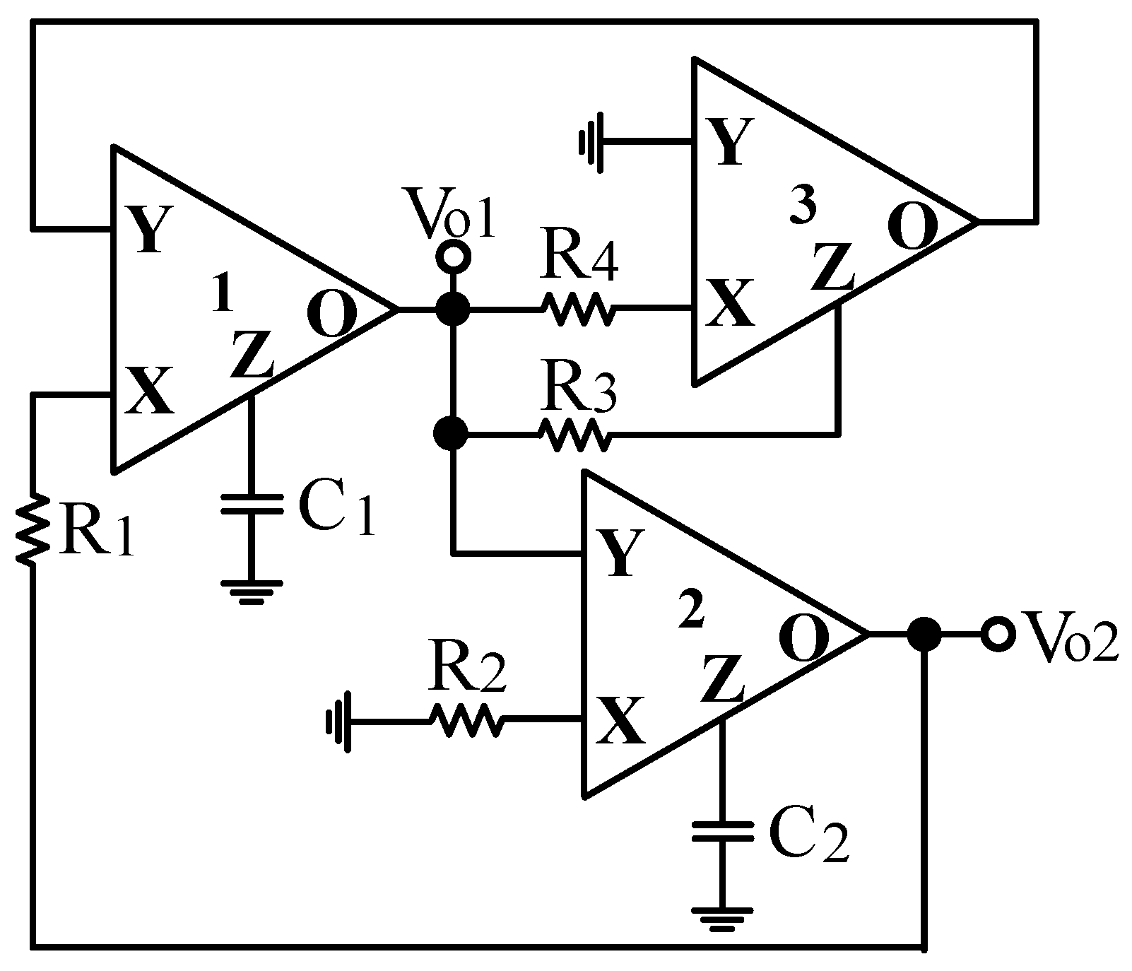
2.2. Proposed Fully-Uncoupled VM QO

Based on the VM multifunction biquad filter structure in Figure 2, the input signal Vin is grounded, the grounding resistor R3 is floating, and the floating terminal of the resistor R3 is connected to the output voltage signal Vo1. Thus, the CFOA-based VM multifunction biquad filter can be transferred to the VM fully-uncoupled QO as shown in Figure 4. Routine analysis of the proposed VM fully-uncoupled QO results in the following characteristic equation.
s 2 + s 1 C 1 R 1 ( R 3 R 4 1 ) + 1 C 1 C 2 R 1 R 2 = 0
According to Equation (10), the CO and FO of Figure 4 are obtained as:
CO :   R 3 R 4
FO :   ω o = 1 C 1 C 2 R 1 R 2
Equations (11) and (12) illustrate that by controlling R3 and/or R4, CO can be tuned fully independently without affecting FO. Similarly, by controlling R1 and/or R2, FO can be tuned fully independently without affecting CO. This means that both CO and FO can be fully-uncoupled controlled by adjusting two sets of completely different resistors. The QO output voltages Vo1 and Vo2 are given by
V o 1 = sC 2 R 2 V o 2
In the steady state, the QO output voltages Vo1 and Vo2 are expressed as
V o 1 = ω o C 2 R 2 e j φ V o 2
where the phase difference φ = 90° to ensure that the output voltages, Vo1 and Vo2 are in quadrature phase shifted.
From Equation (14), the magnitude ratio of the quadrature output voltages Vo1 and Vo2 is given by
| V o 1 V o 2 | = ω o C 2 R 2 = C 2 R 2 C 1 R 1
Assuming that C1 = C2 and R1 = R2, the magnitude ratio of the QO output voltages Vo1 and Vo2 in Equation (15) becomes
| V o 1 V o 2 | C 1 = C 2 ,   R 1 = R 2 = 1
Equation (16) describes that the phase shift of the two quadrature output voltages is 90°, and the magnitude ratio of two quadrature output voltages is also equal. Thus, the proposed VM fully-uncoupled QO solves the amplitude instability and improves the unbalance of the generated quadrature output amplitudes Vo1 and Vo2. When tuning FO, the constant amplitude ratio of two quadrature sinusoidal waveforms can be realized. Hence, the proposed VM fully-uncoupled QO is advantageous to the stability of the combined amplitude.
The phase noise figure-of-merit (FoM) for oscillators summarizes the important performance parameters. The conventional phase noise FoM of the oscillators is defined as follows [33].
FoM ( Δ ω ) = L ( Δ ω ) + 20 log ( ω o Δ ω ) 10 log ( P DC 1 mW )
where Δω is the offset frequency relative to the carrier, ωo is the oscillation frequency, and L(Δω) is the phase noise at the offset frequency to the carrier. PDC is the power (in mW) consumed by the oscillator. In order to estimate FoM of the proposed VM fully-uncoupled QO, the phase noise FoM will be discussed in the next Section.

3. Simulation and Experimental Results
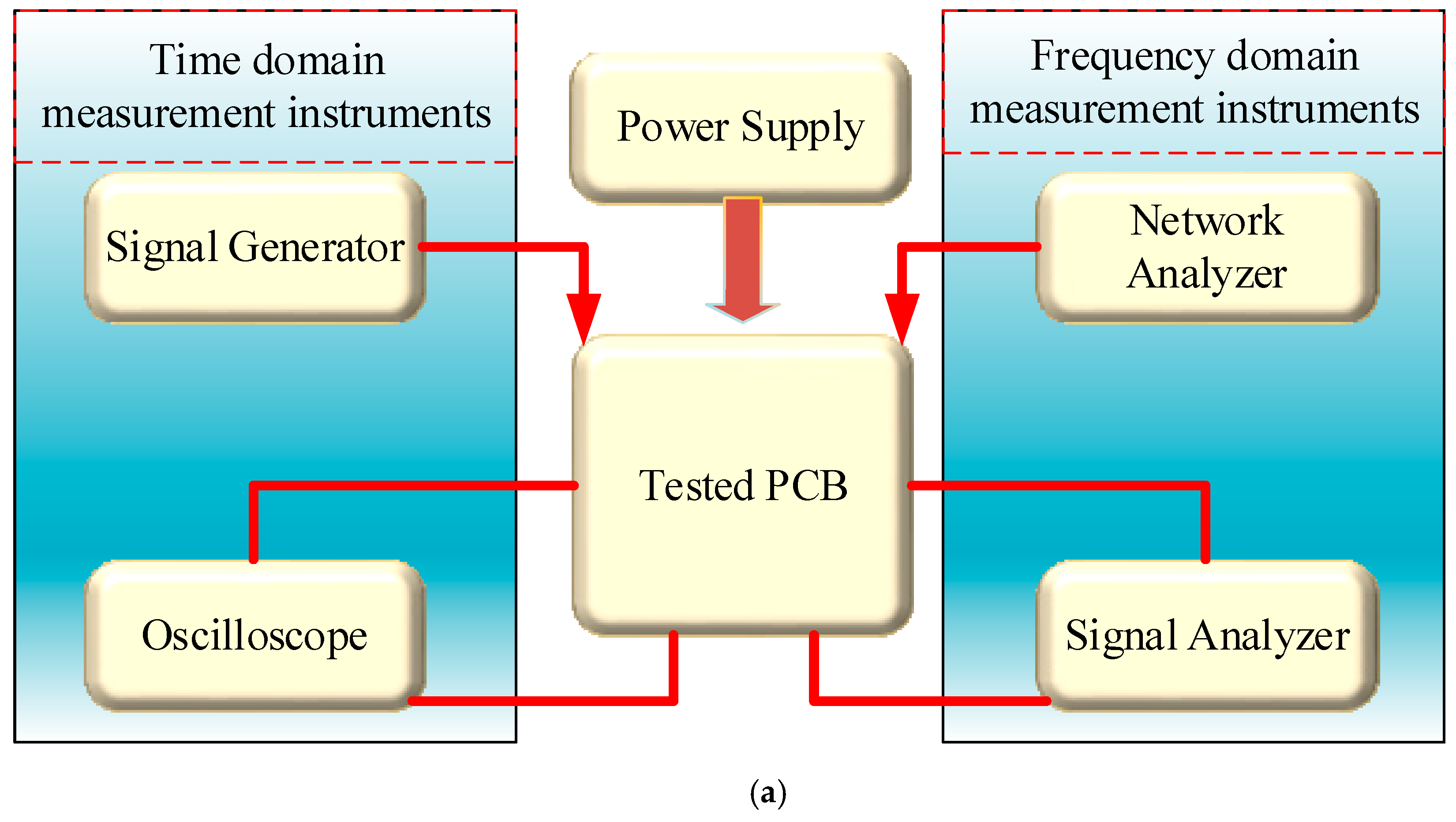
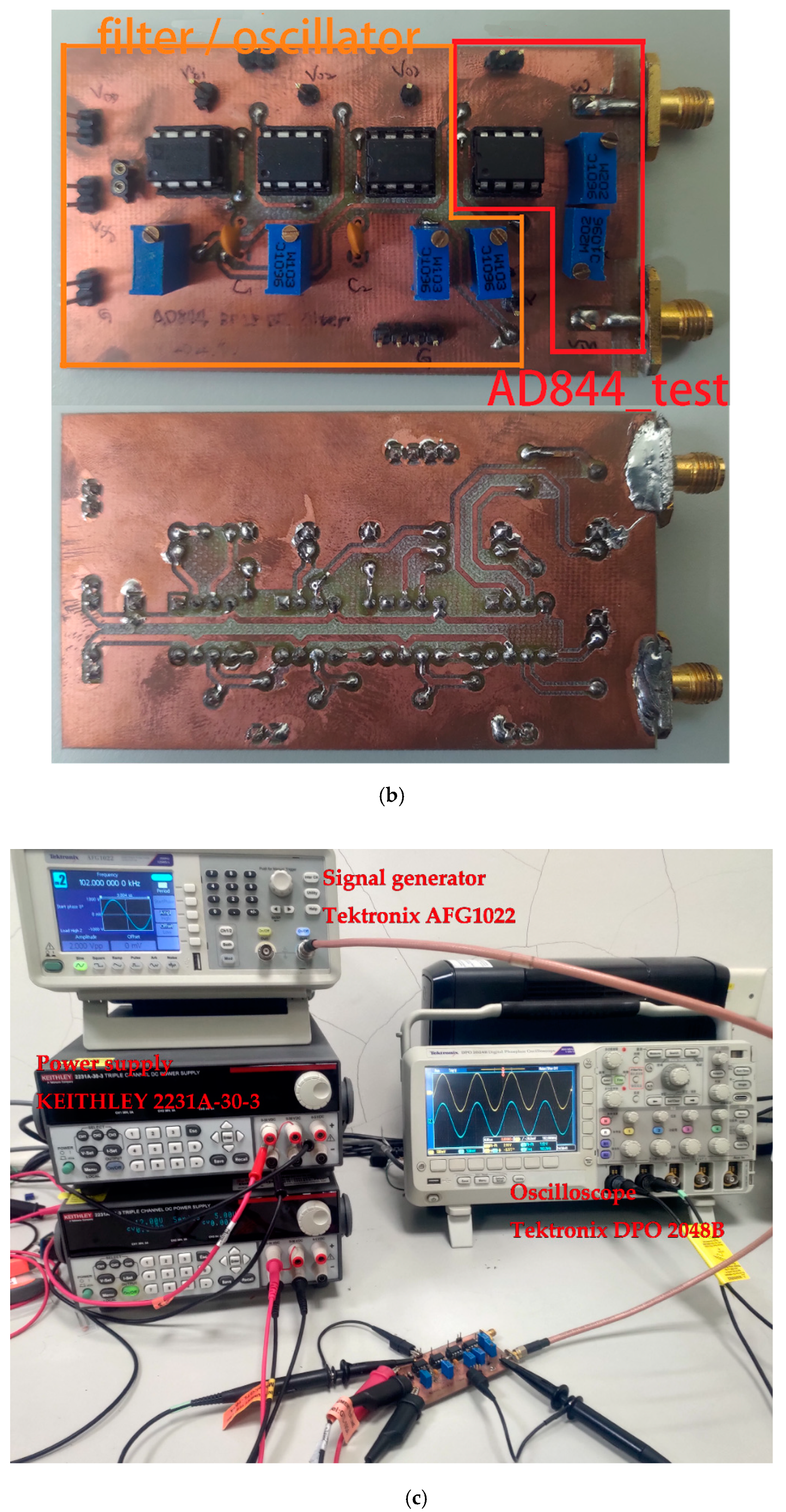
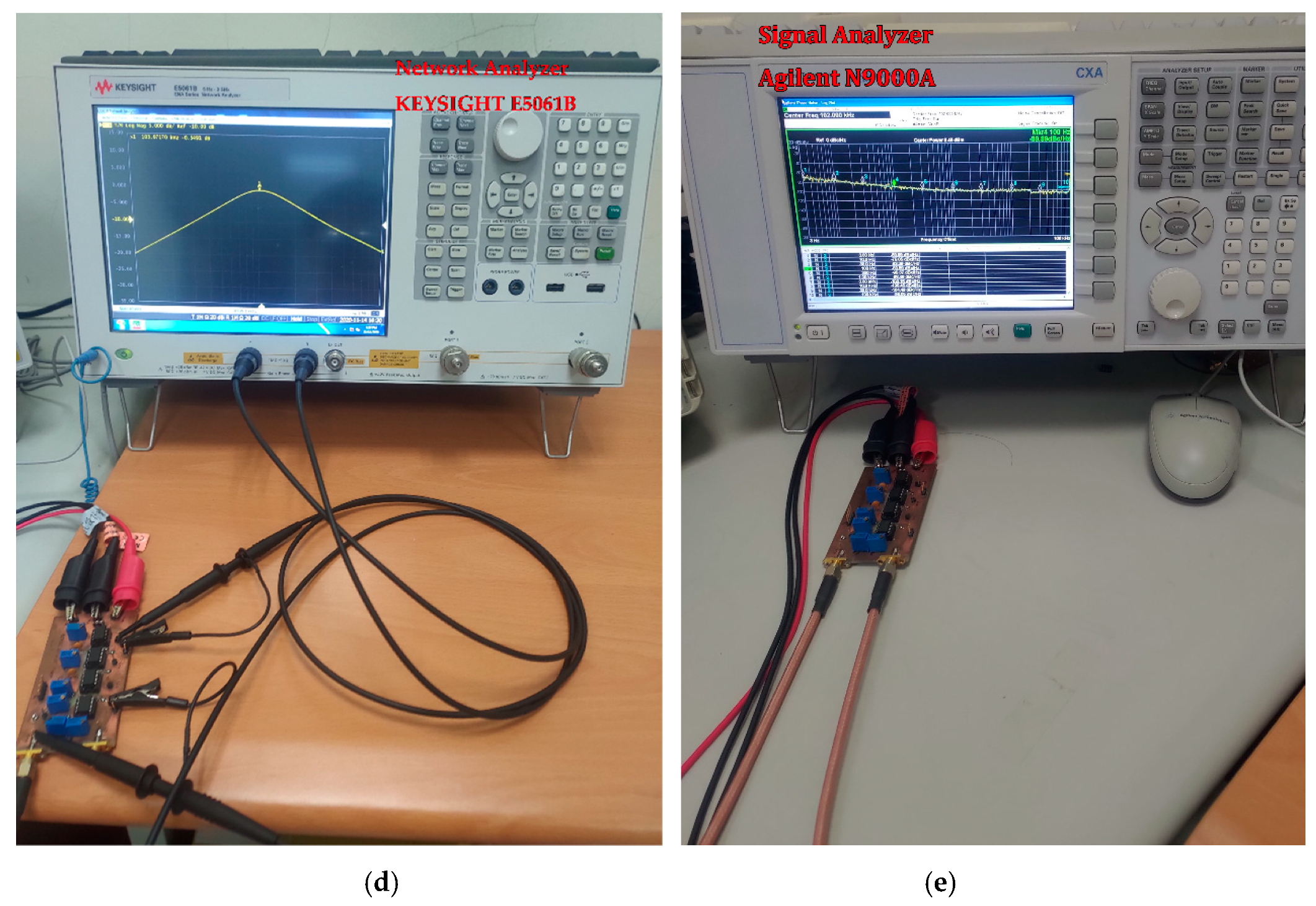
3.1. Test Setup

In order to use the commercial AD844AN IC to prove the real behavior of the proposed VM multifunction biquad filter and fully-uncoupled QO, an experimental test bench was developed, as shown in Figure 5. In Figure 5, the experimental setup uses a printed circuit board (PCB), DC power supply voltage, signal generator, oscilloscope, network analyzer, and signal analyzer. Keithley 2231A-30-3 power supply provides DC power supply voltage to PCB. The time domain of the filter and the output voltage swing of the oscillator are measured by the Tektronix DPO 2048B oscilloscope, and a Tektronix AFG1022 signal generator is used to generate the input signal of the filter. The frequency domain of biquad filter responses is measured by Keysight E5061B-3L5 network analyzer. One dB power gain compression point (P1dB), intermodulation distortion (IMD), phase noise, and output frequency spectrum are measured by the Keysight-Agilent N9000A CXA signal analyzer.

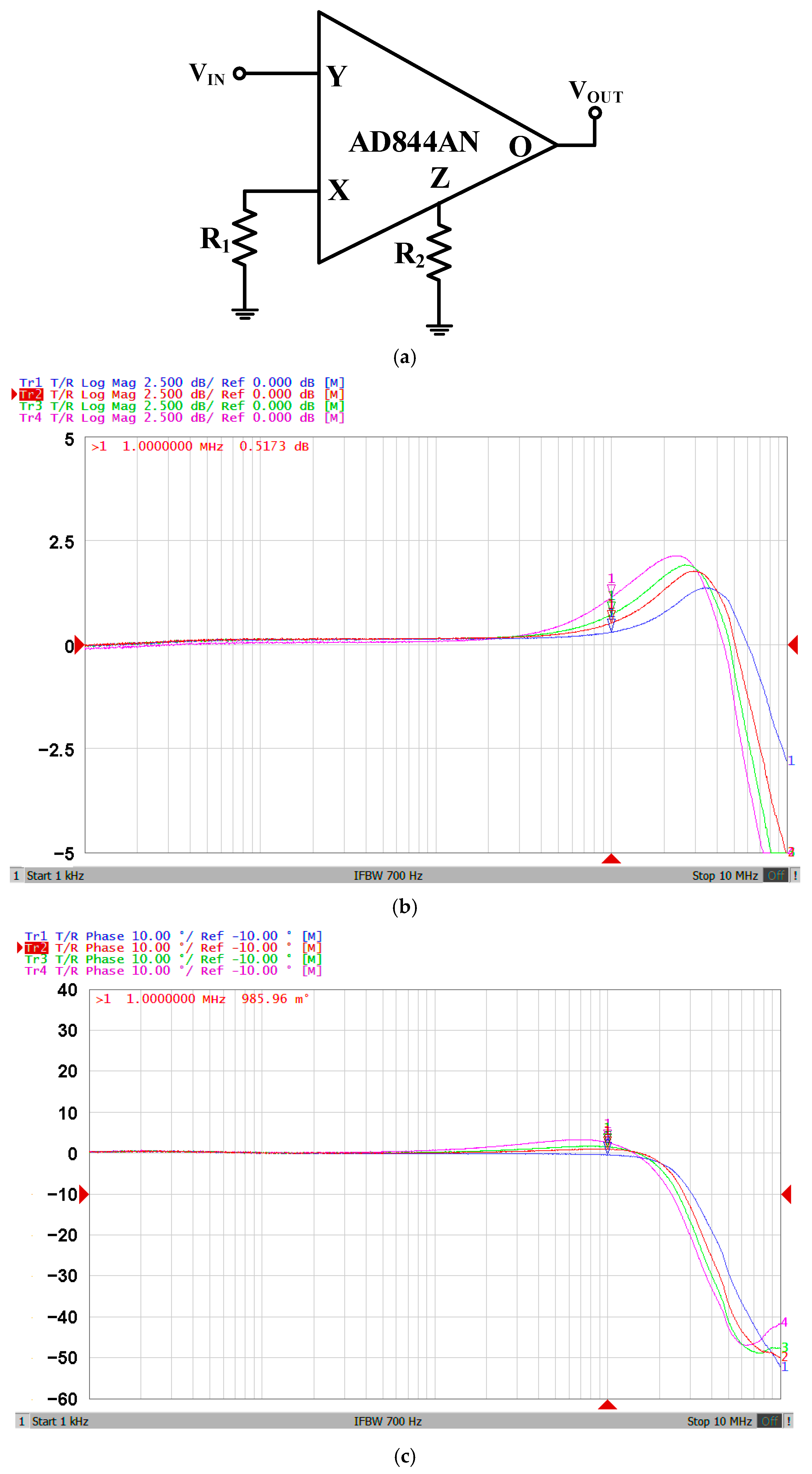
3.2. Effective Frequency Ranges of AD844AN-Based Circuit

The proposed VM multifunction biquad filter and fully-uncoupled QO circuits are simulated by Cadence OrCAD PSpice version 16.6 software. The model parameters of CFOA come from the built-in library AD844/AD. Programming using Intel Core i5-8400 CPU and MATLAB version 2019a has confirmed the effectiveness of simulation and theoretical analysis. For the experiments, the proposed CFOA-based VM multifunction biquad filter and fully-uncoupled QO circuits use AD844AN ICs. The supply voltages for simulation and experiment are ±6 V. In general, the applicability of such filters and oscillators based on CFOA circuits and using AD844AN ICs is usually limited to a few hundred kilohertz [31,32]. To test the frequency ranges of AD844AN, the test circuit based on AD844AN is shown in Figure 6. The supply voltages are ±6 V. In Figure 6a, the selected resistance values are R1 = R2 = R = 2 kΩ (4 kΩ, 6 kΩ, 10 kΩ). Figure 6b shows the measured gain responses of the AD844AN characteristics. Figure 6c shows the measured phase responses of the AD844AN characteristics. As shown in Figure 6, the frequency range of the AD844AN-based circuit is limited to 1 MHz.

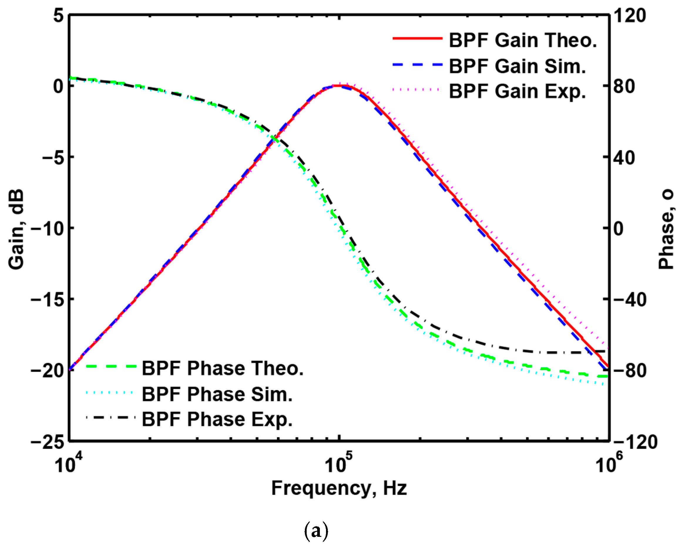
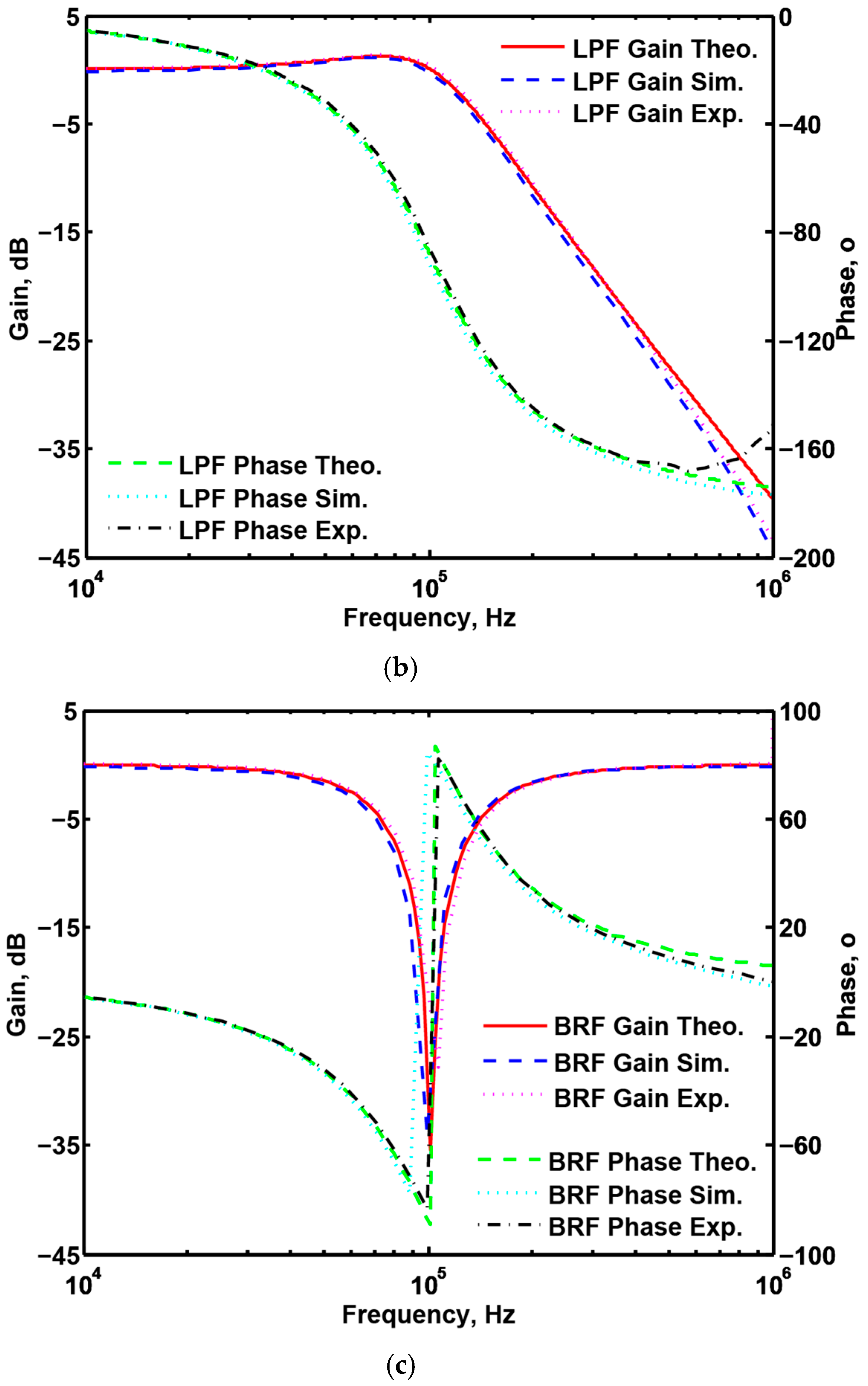
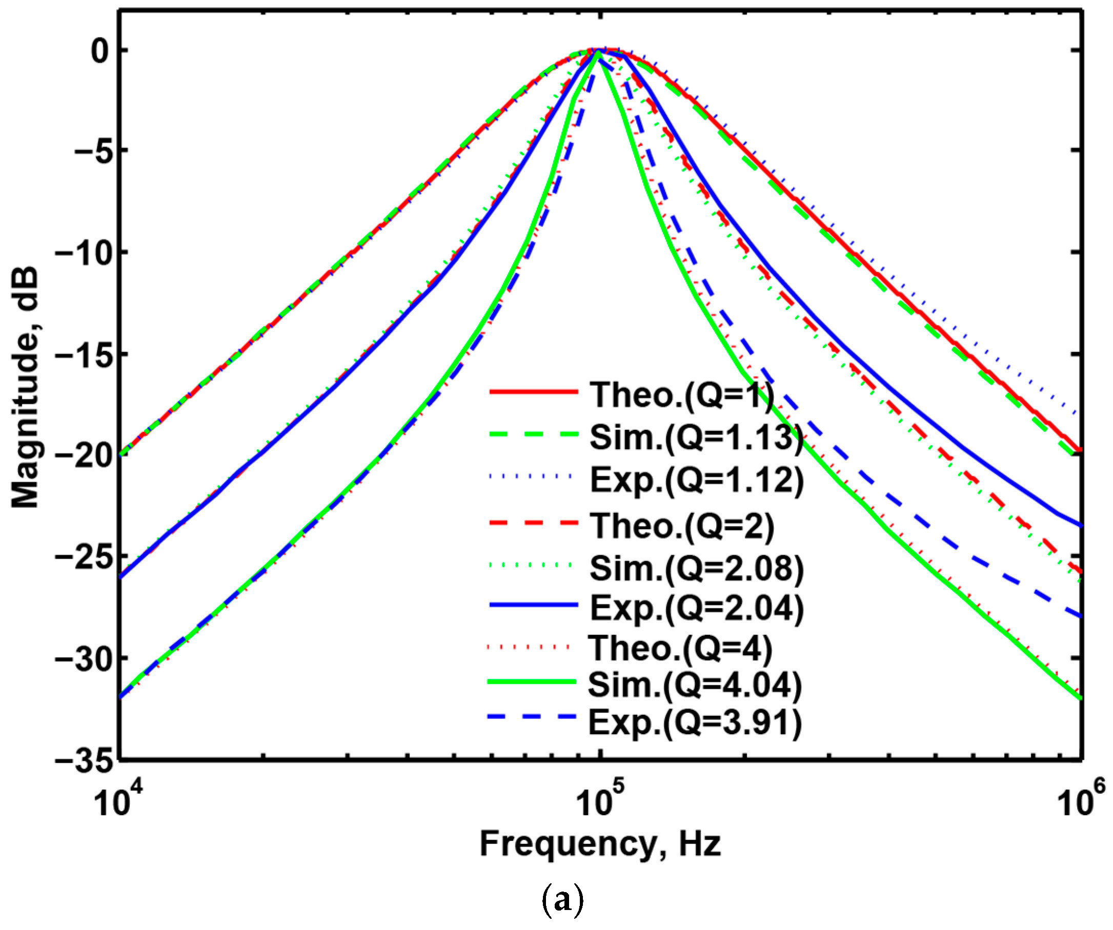
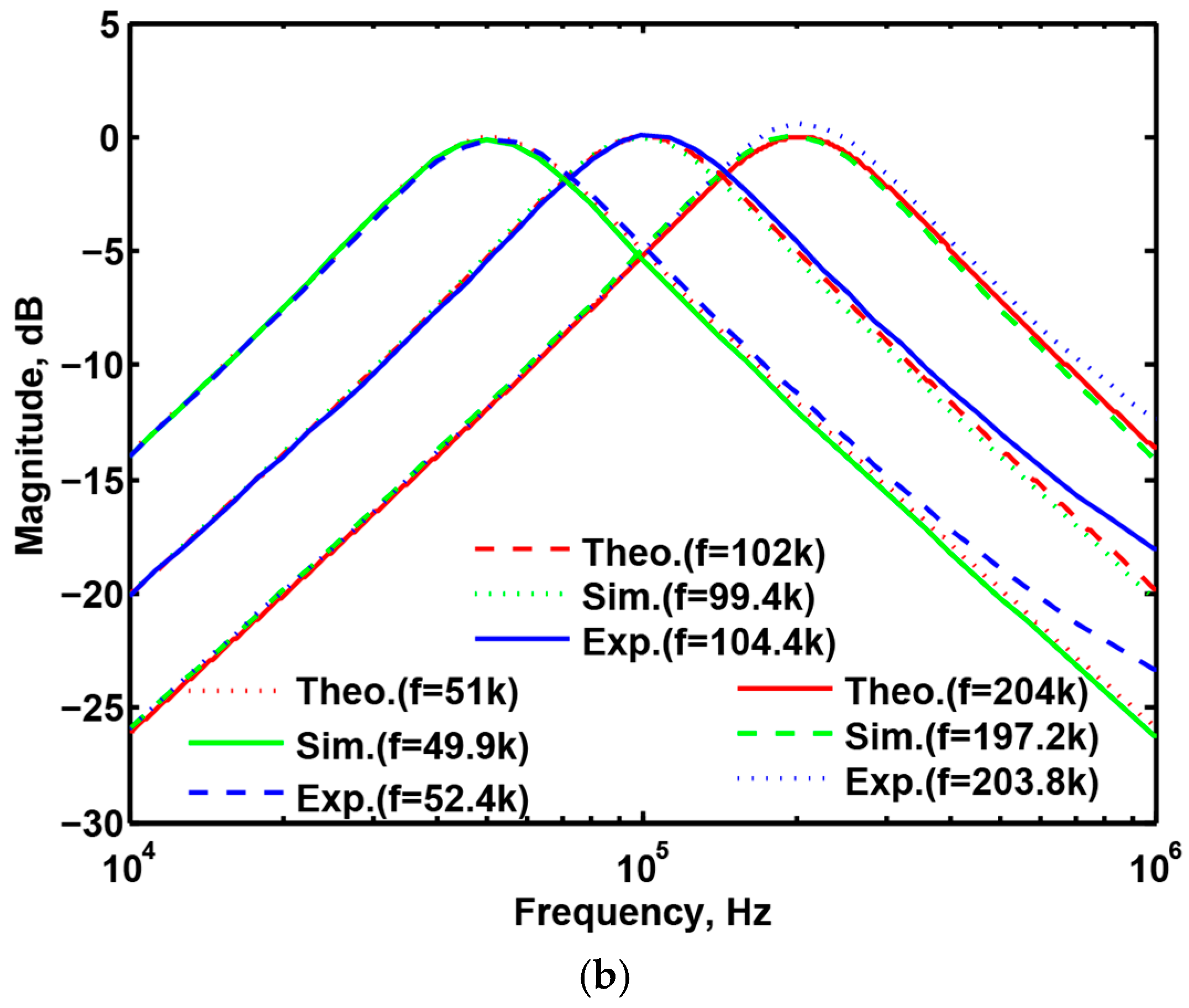
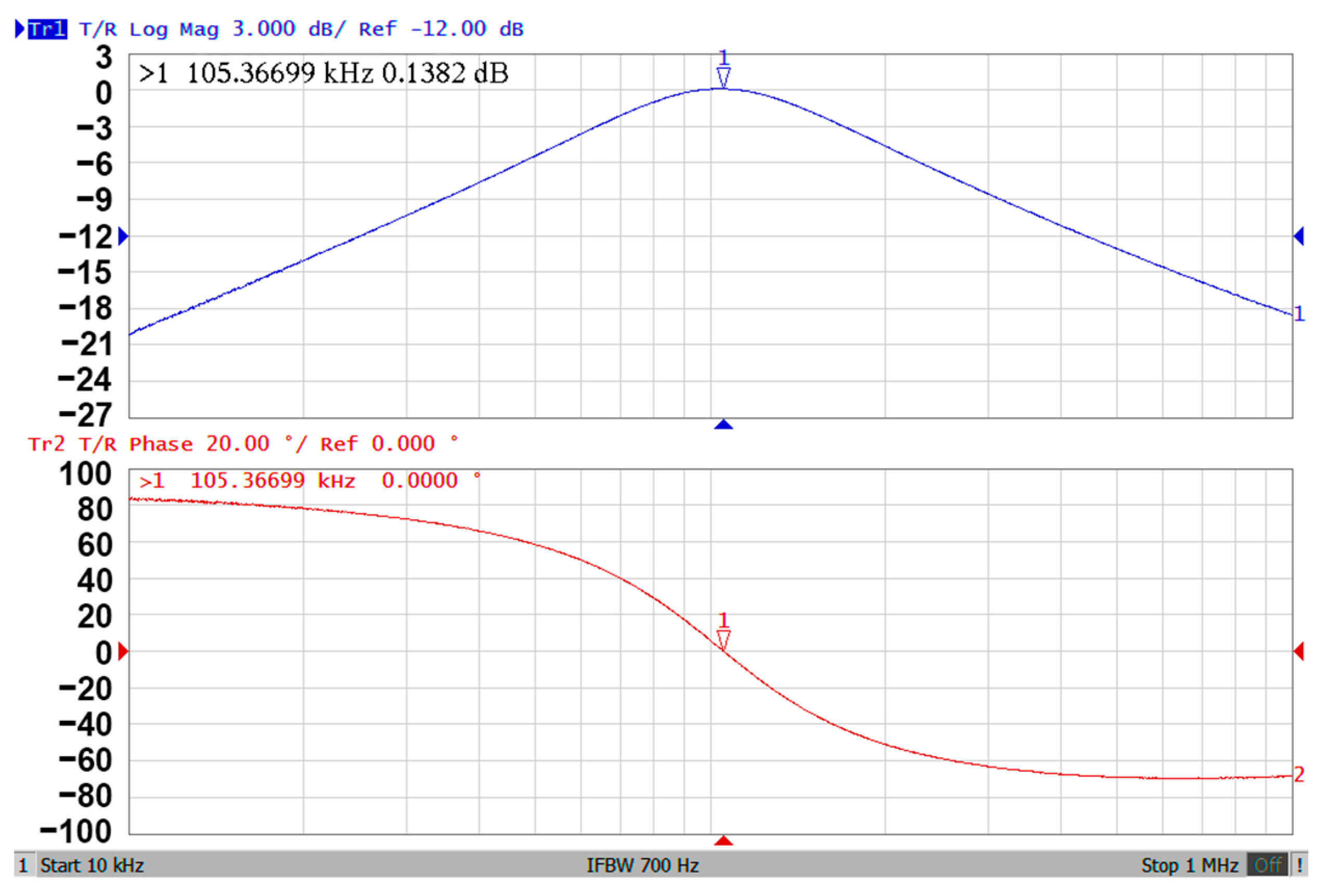
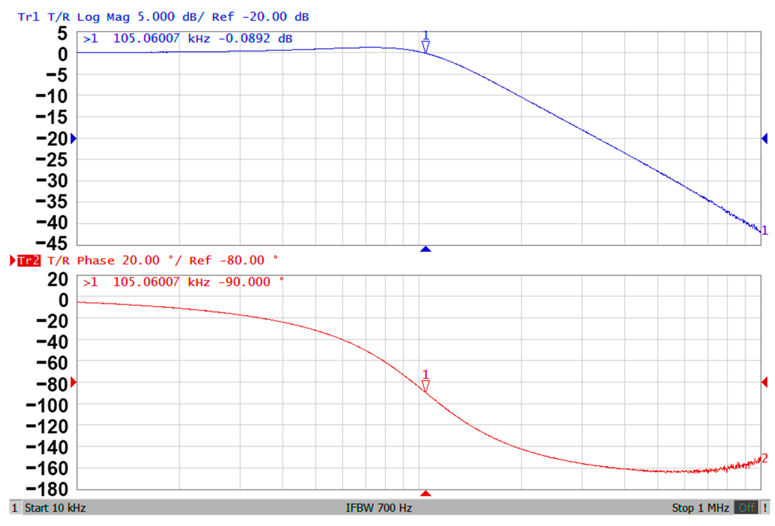
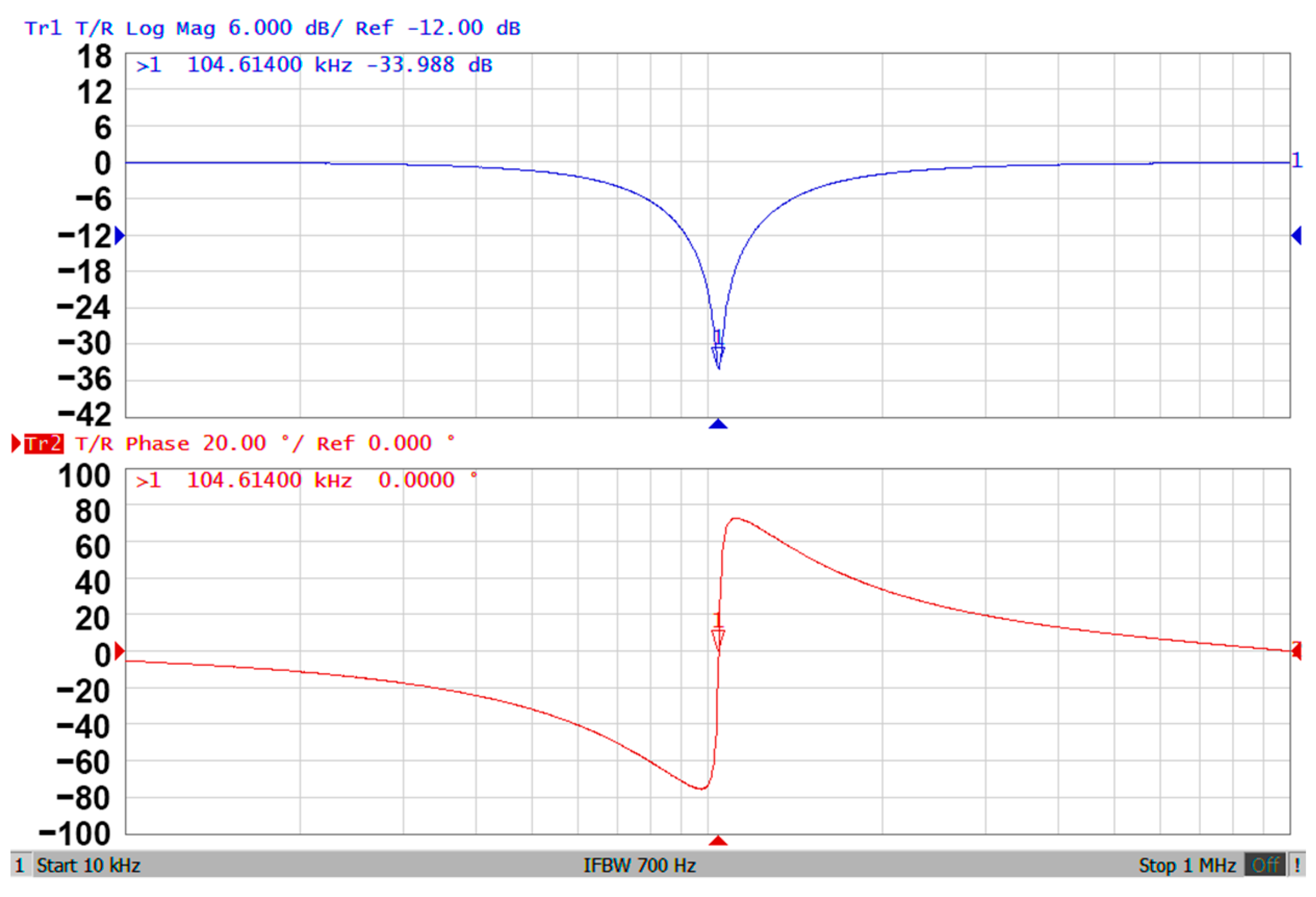
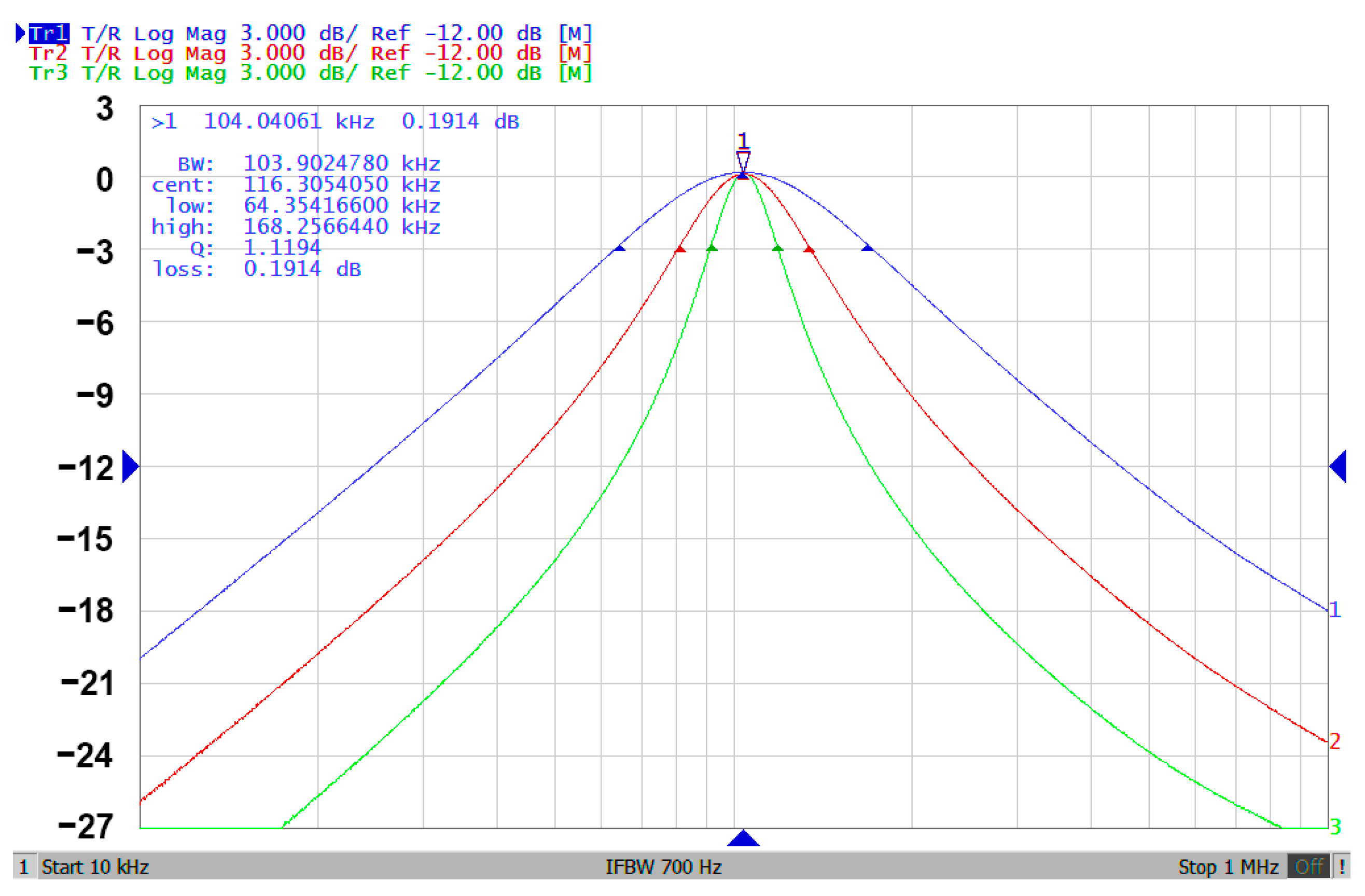
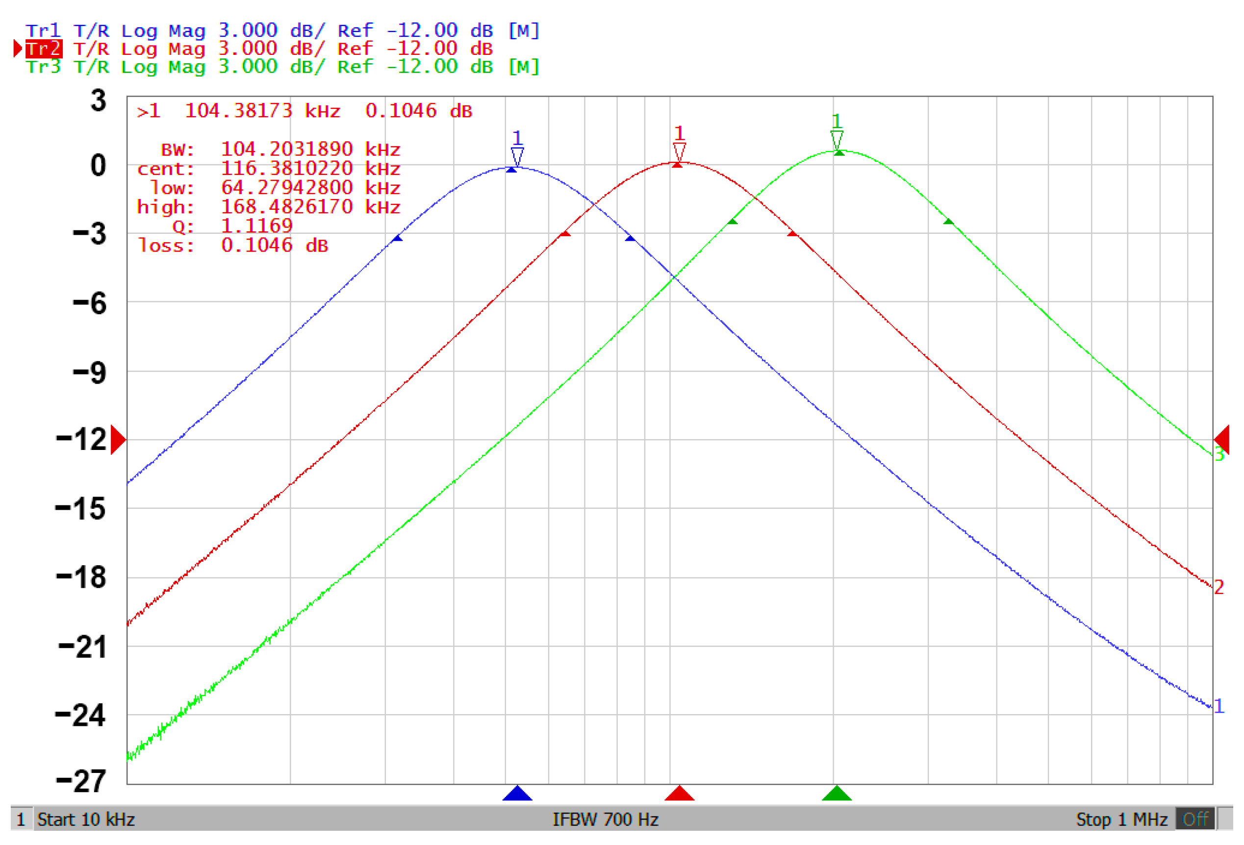
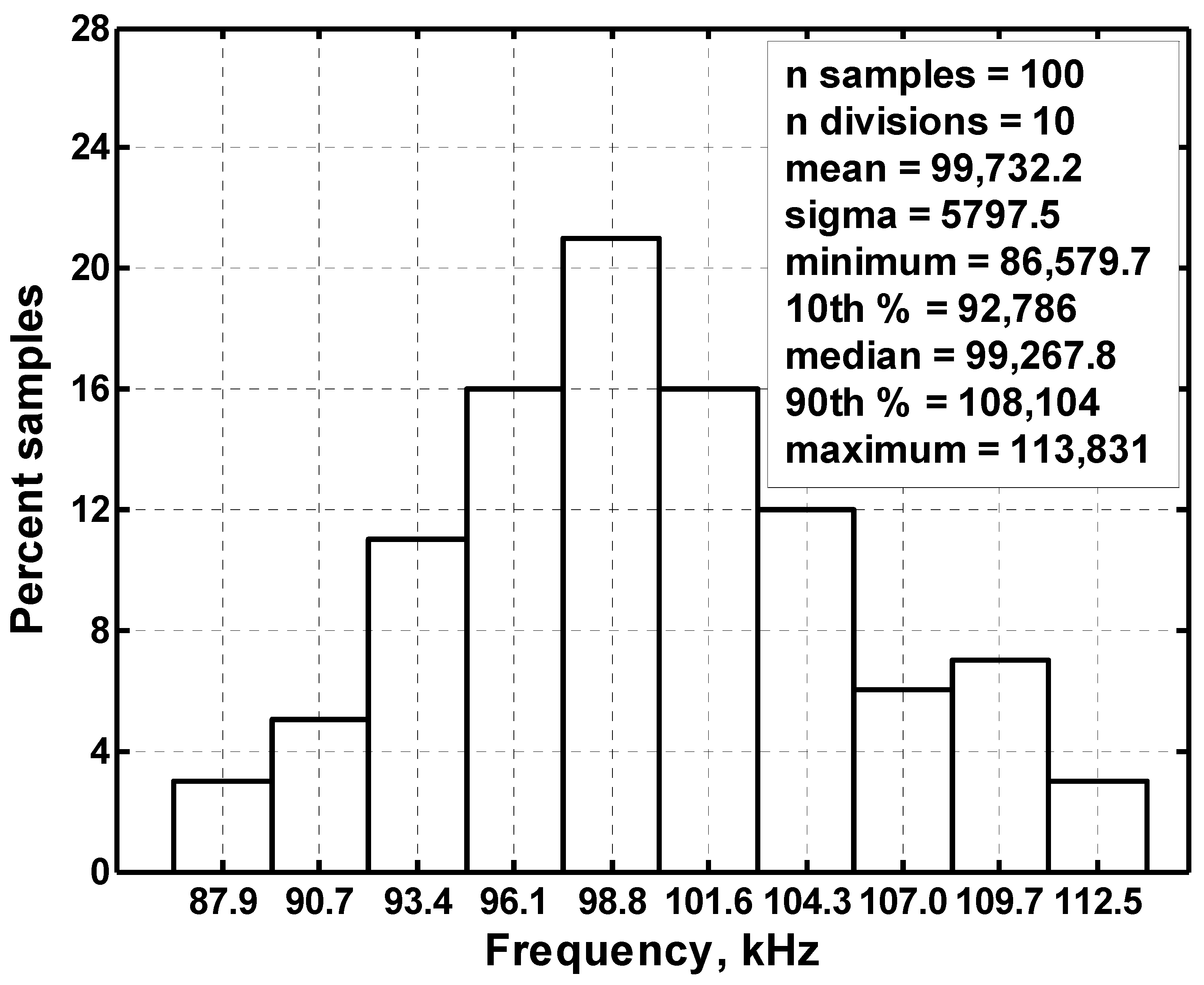
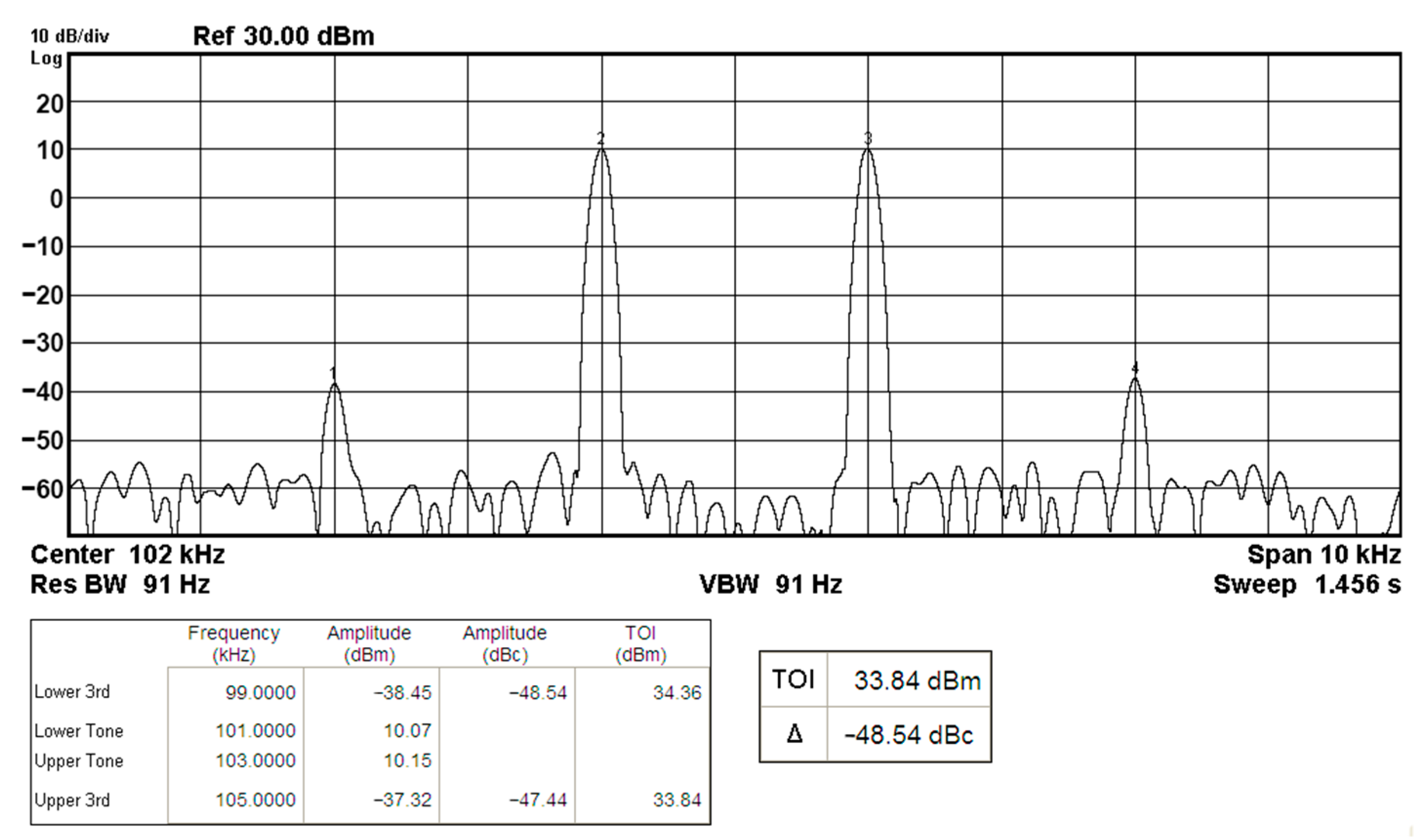
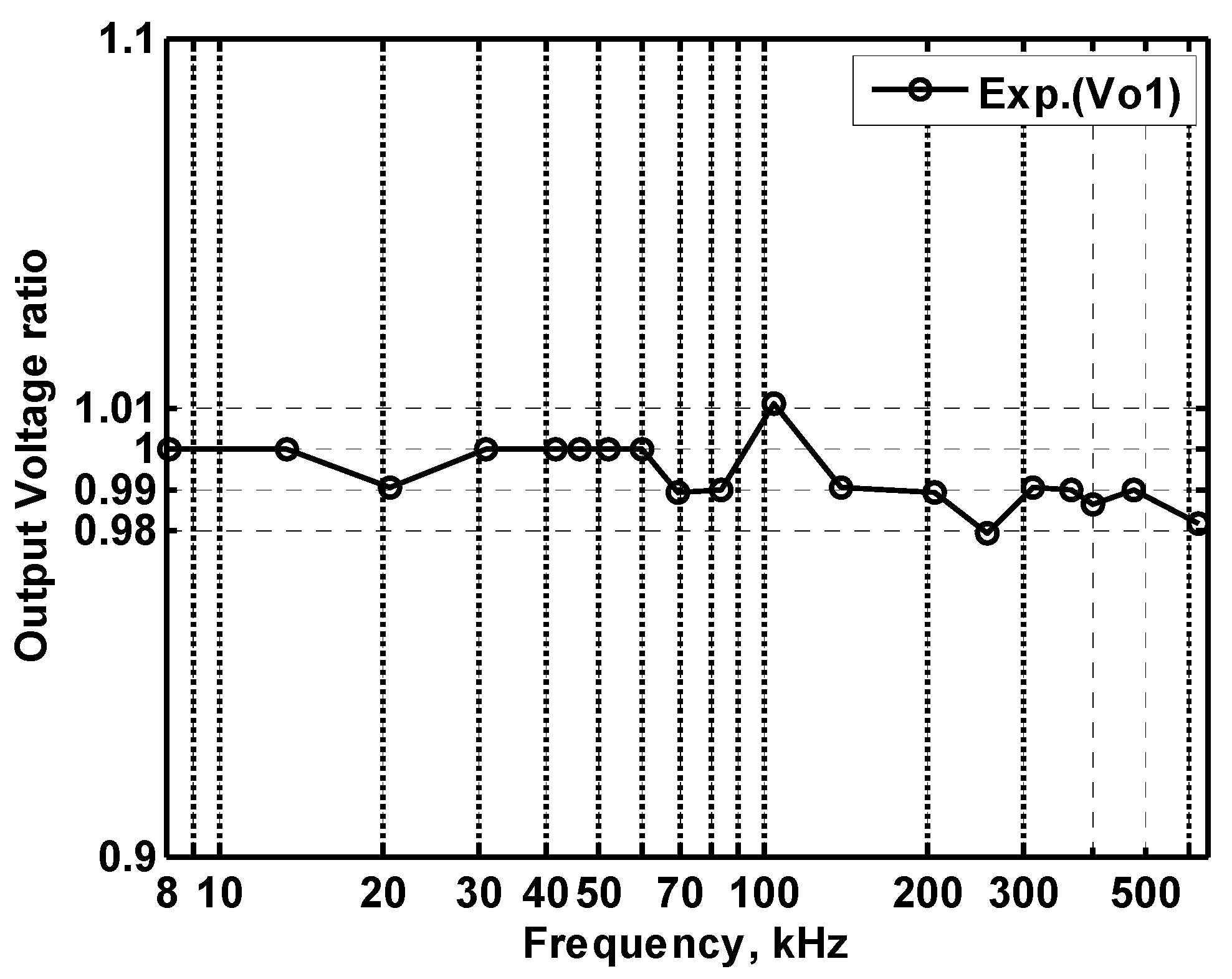
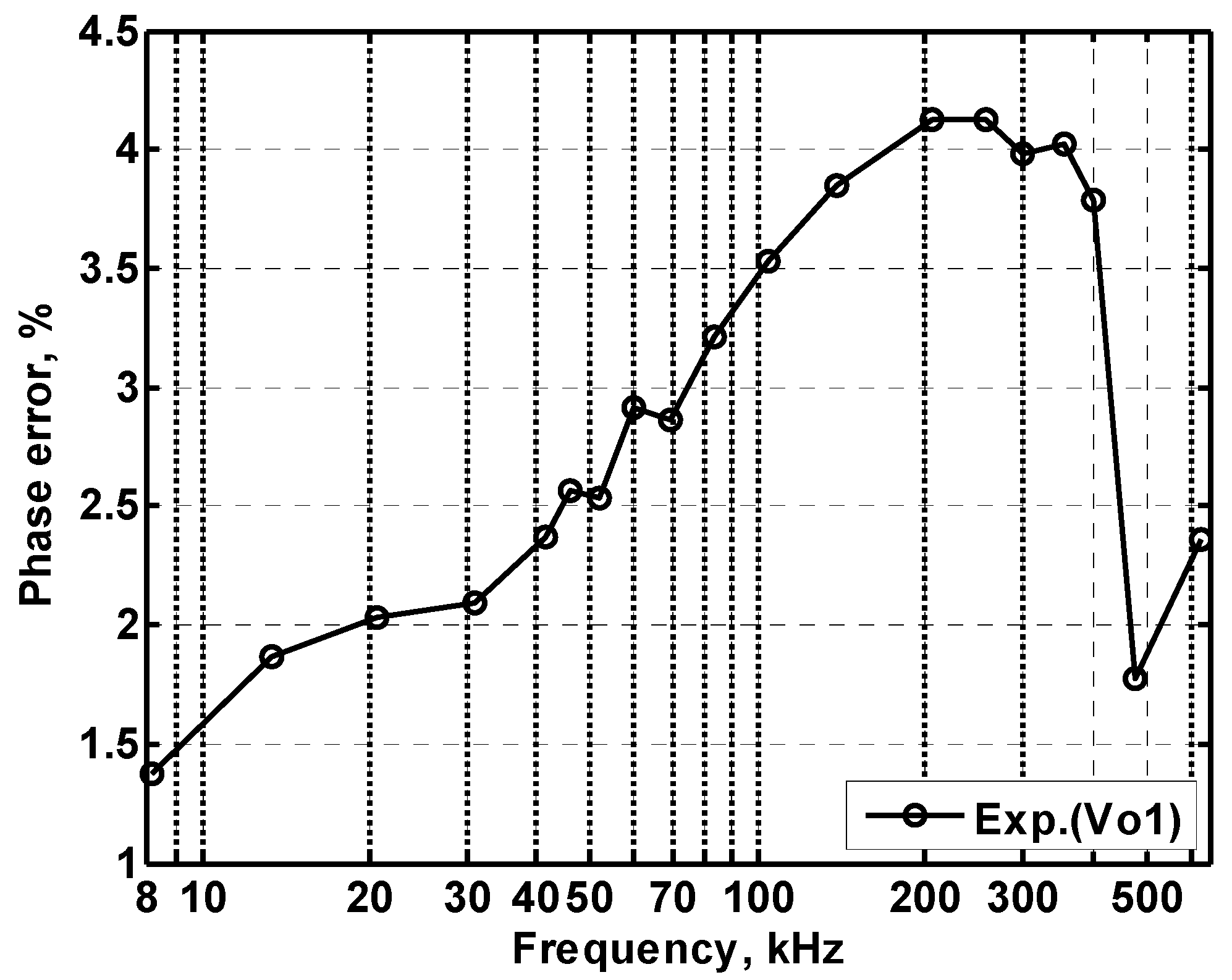
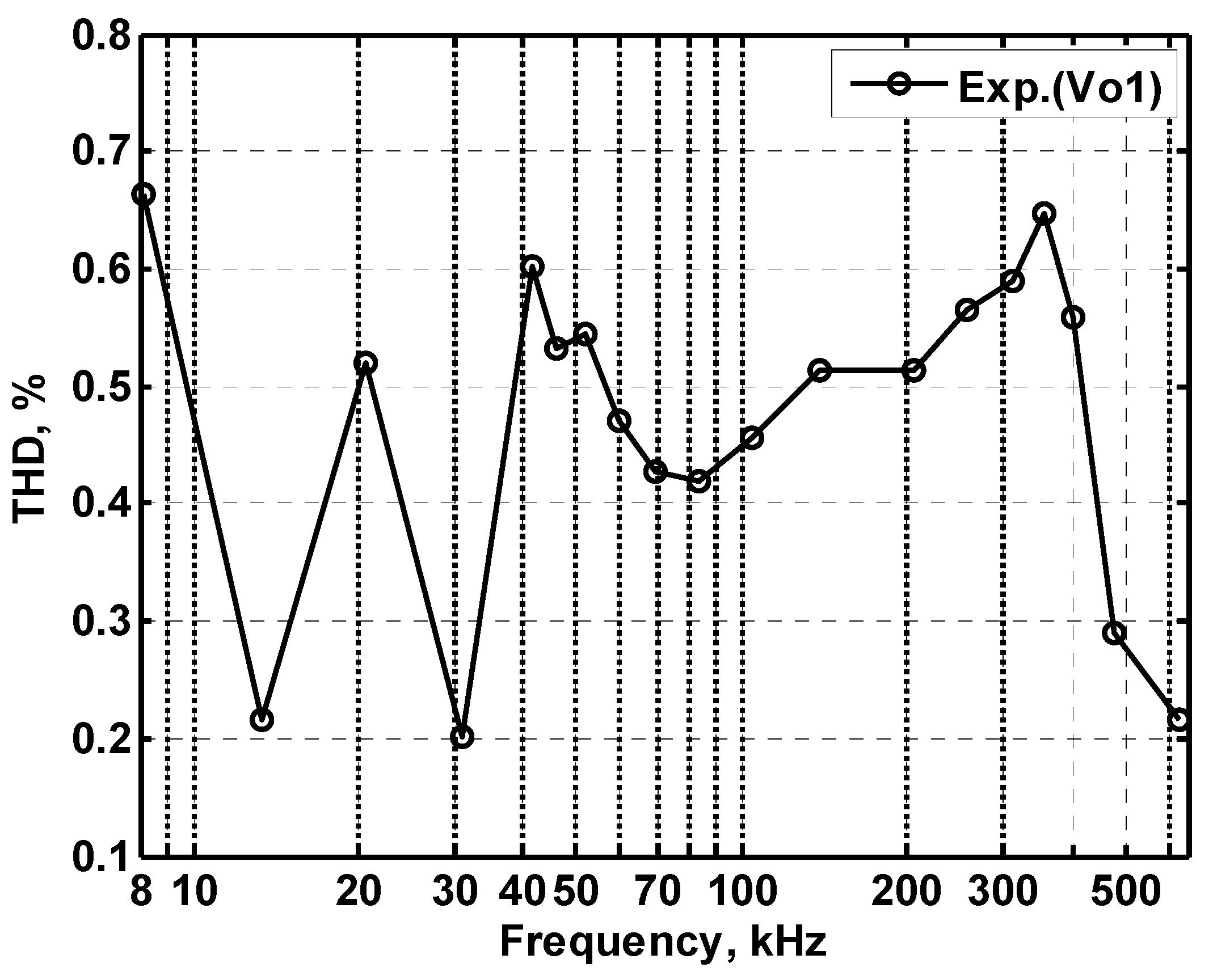
3.3. Proposed CFOA-Based VM Multifunction Biquad Filter

To validate the theoretical study of Figure 2, Figure 7a–c show the simulation and experimental results of the BPF, LPF and BRF with the theory responses, respectively. In Figure 7, the values of passive elements are selected as C1 = C2 = 390 pF and R1 = R2 = R3 = R4 = 4 kΩ. The selection of these values is to obtain a VM multifunction biquad filter with a center frequency of fo = 102 kHz and a quality factor of Q =1. The total power consumption of the simulation and experimental results is about 255 mW and 168 mW, respectively. By keeping the values of C1 = C2 = 390 pF, R1 = R2 = R3 = 4 kΩ, the control factor parameter Q of the characteristic filter can be tuned without disturbing fo. When the value of R4 changes between 16 kΩ, 8 kΩ, and 4 kΩ, this resulted in BPF responses are shown in Figure 8a. Similarly, by keeping the values of C1 = C2 = 390 pF, R3 = R4 = 4 kΩ, the control factor parameter fo of the characteristic filter can be tuned without disturbing Q. When Q = 1, and R1 and R2 are varied between 8 kΩ, 4 kΩ, and 2 kΩ, this resulted in BPF responses are shown in Figure 8b. This range is dependent on the bandwidth of AD844AN. Figure 8a,b show the CFOA-based multifunction biquad filter, whose filter control factor parameters Q and fo have independent tuning capabilities. Figure 9, Figure 10 and Figure 11 show the measured BPF, LPF and BRF responses obtained by a network analyzer, respectively. Figure 12 and Figure 13 show the measured gain responses of Q and fo respectively, as explained in Equation (5). In order to compare the theoretical analysis, the authors derived the measurement data of Figure 9, Figure 10, Figure 11, Figure 12 and Figure 13 and added them as additional traces to Figure 7a–c and Figure 8a,b, respectively. As can be seen, the simulation and experimental results are consistent with the theoretical values. However, the real active components have non-ideal characteristics, such as the parasitic impedance effect of AD844AN, the non-ideal characteristics caused by the frequency dependence of the internal voltage and current transmission of the AD844AN, and the parasitic impedance effect of PCB layout issue. These additional parasitic resistances and capacitances of the AD844AN, the PCB layout issue, and the tolerances of the working resistors and capacitors will have main effects on circuit accuracy.
The Monte Carlo analysis method is used to study the VM CFOA-based multifunction biquad filter. Statistical analysis of Monte Carlo 100 simulation can be performed. Figure 14 shows the histogram of center frequency obtained from the Monte-Carlo analysis of the BPF response in Figure 2. The resistor and capacitor values in Figure 2 are chosen as 4 kΩ and 390 pF, respectively, and the Gaussian variation of the resistance and capacitance is 5%. According to Monte-Carlo simulation, the center frequency varies between 86.6 and 113.8 kHz and the fo value of the BPF response is affected in the range of −15.1% to 11.6%.
To obtain the input dynamic range of the proposed CFOA-based VM multifunction biquad filter in Figure 2, the experiment was repeated for a sinusoidal input signal of 102 kHz to show the filter operation in time-domain. Figure 15 shows the input and output voltage waveforms of the experimental BPF. The waveform shows that the amplitude is 6.96 Vpp without signification distortion. The measured center frequency is about 101.8 kHz, which is close to theoretical value of 102 kHz with −0.2% error rate. To illustrate the linear range of the circuit, P1dB is an important parameter for evaluating linear range of the circuit, when the output is saturated in the circuit. This is defined as the input power that results in the circuit gain to decrease by 1 dB. Input and output power gain is the relationship of output power = input power + gain. To evaluate the linear range of the VM biquad filter, consider the BPF, LPF and BRF in Equations (1) to (3). Figure 16 shows the measured P1dB of the BPF at an input power with a center frequency of 102 kHz. The P1dB of the BPF measured at Vo1 is about 22 dBm with respect to input power. The measured linearity performance of P1dB and total power consumption with different input signal voltages are summarized in Table 3. It should be noted that Table 3 is the measurement results of spectrum analysis, whose input impedance is 50 Ω, so the measurement result of output power has slightly attenuated. The parasitic resistances and capacitances of the AD844AN, the PCB layout issue, and the tolerances of the working resistors and capacitors will also have effects on circuit accuracy.
To represent the nonlinearity of the proposed VM multifunction biquad filter proposed in Figure 2, the two-tone test of IMD has been used to characterize the nonlinearity of BPF response. Figure 17 shows the frequency spectrum analysis of BPF through intermodulation characteristics by applying two-tone signals, f1 and f2, around the corner frequency of fo = 102 kHz. In Figure 17, a low-frequency tone of f1 = 101 kHz and a high-frequency tone of f2 = 103 kHz are used with equal input amplitudes of 4.5 Vpp. As shown in Figure 17, the measured value of the third-order IMD is around −48.54 dBc, and the third-order intercept (TOI) point is around 33.84 dBm.

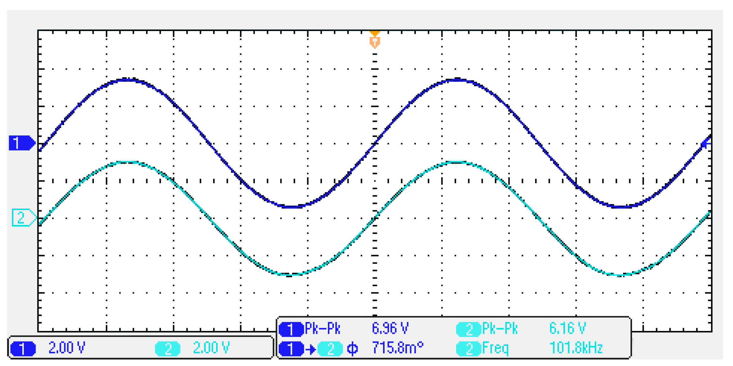
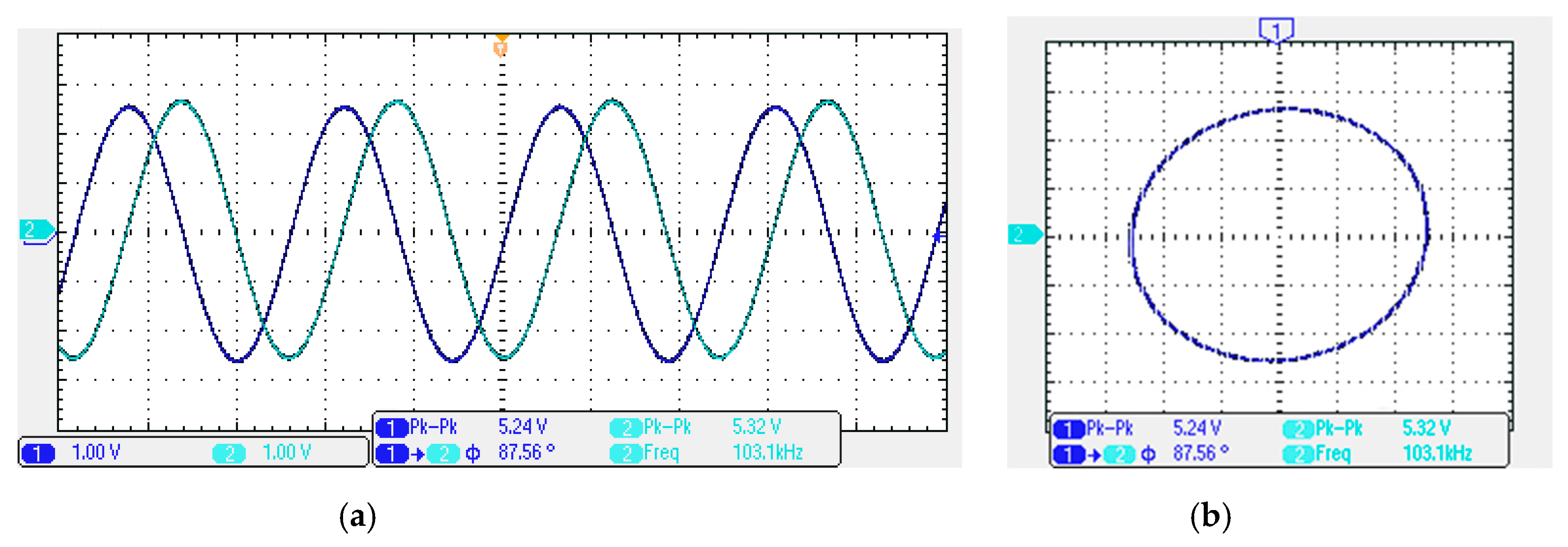
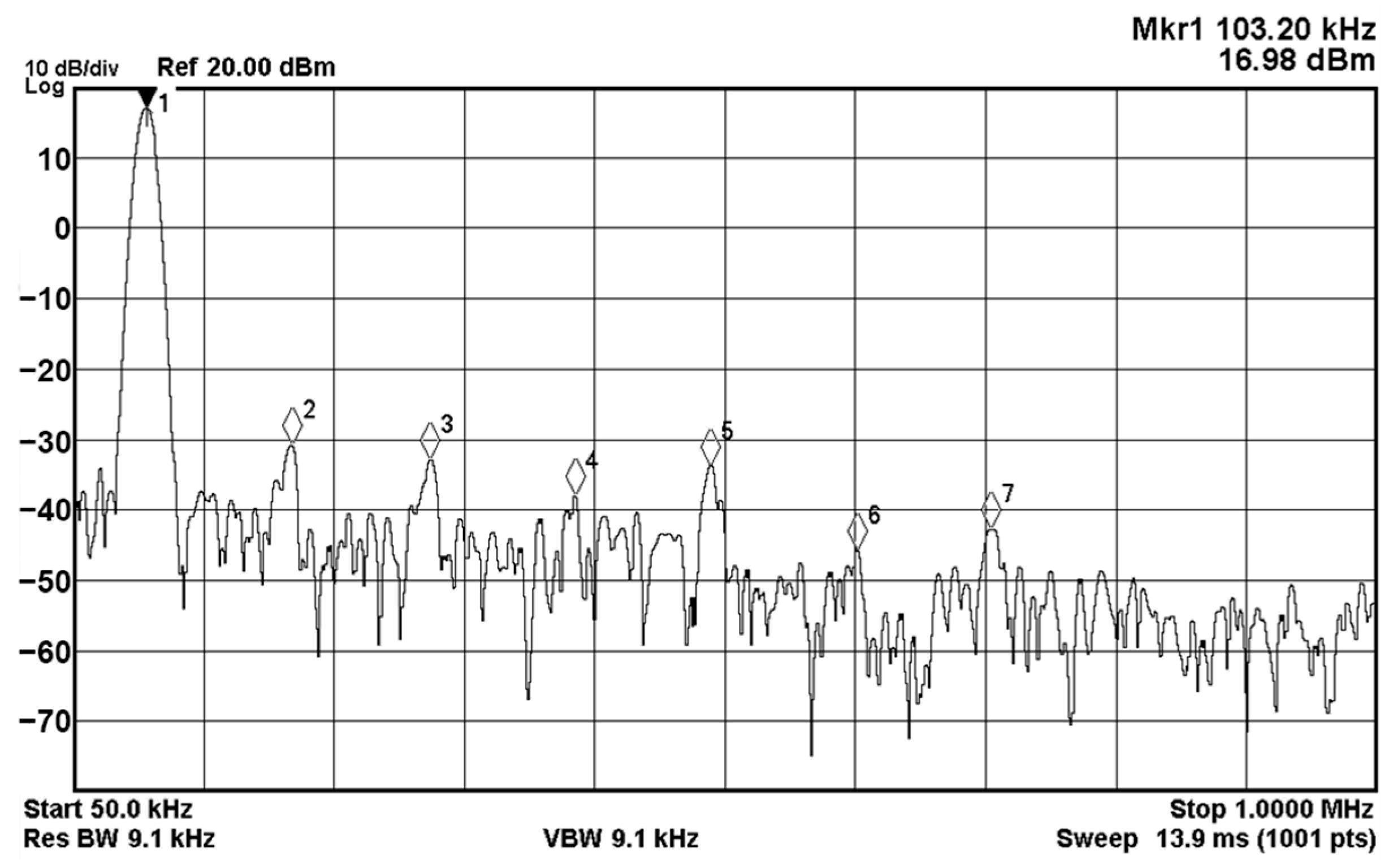
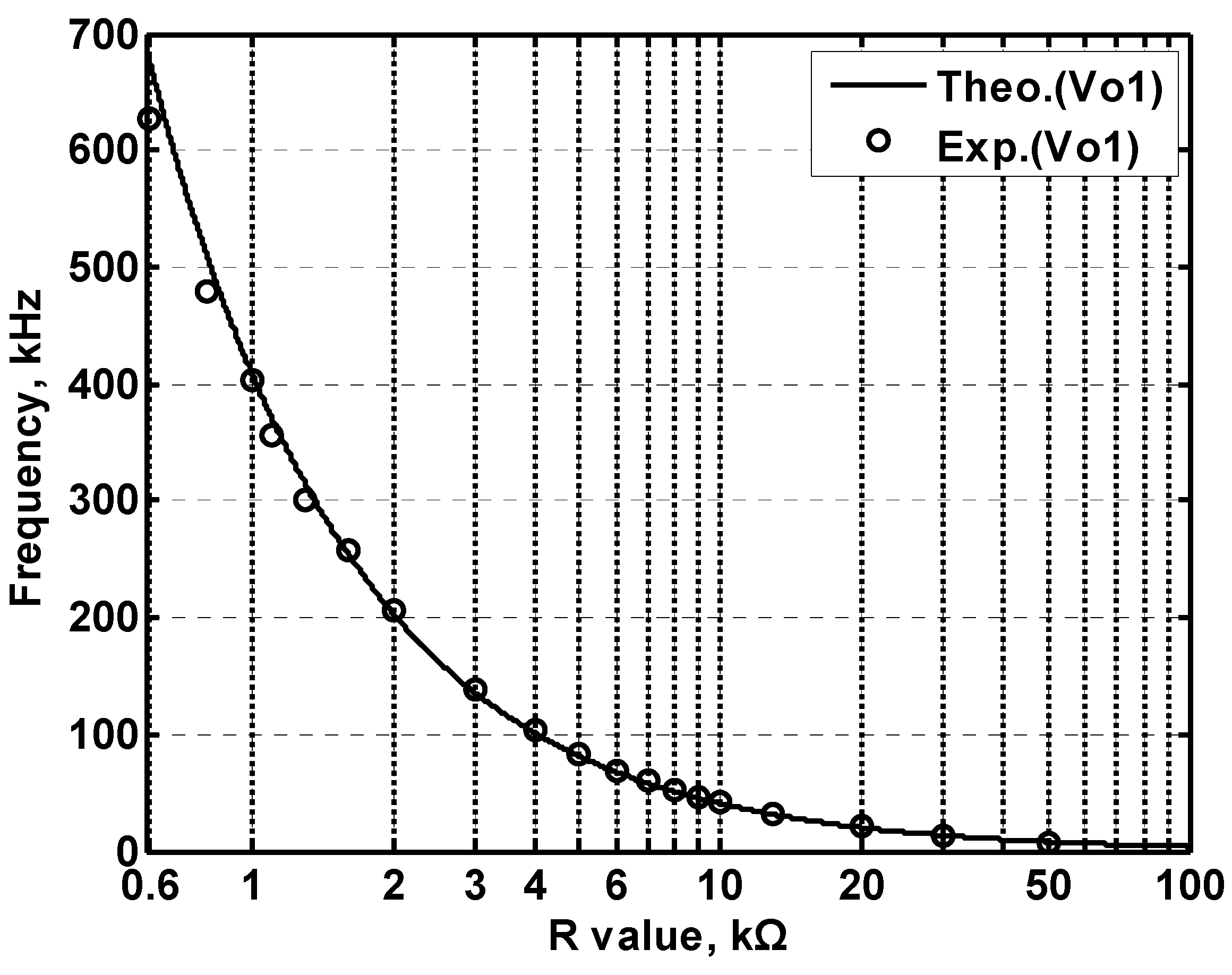
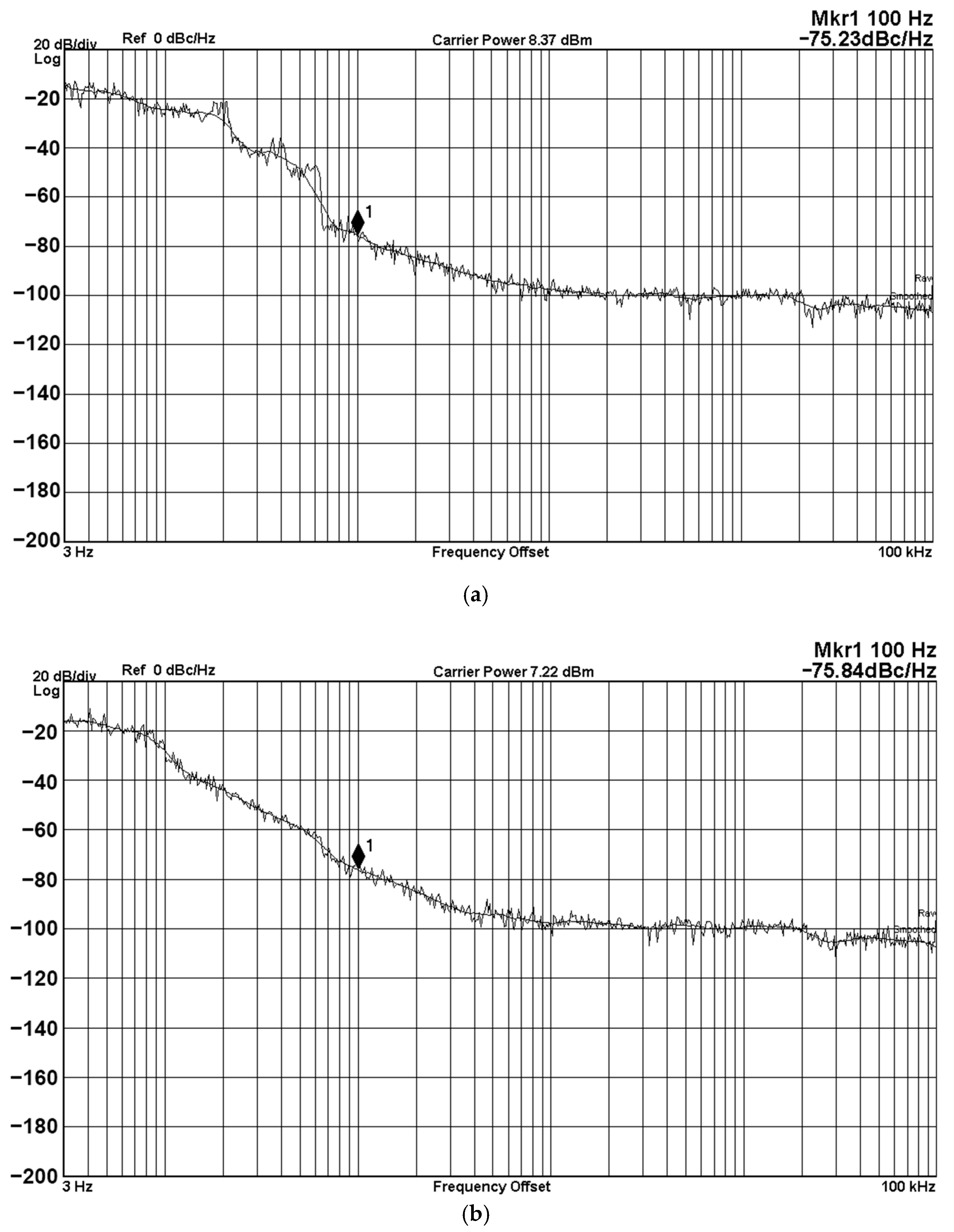
3.4. Proposed CFOA-Based VM QO Experimental Results

In order to get the theoretical oscillation frequency fo = 102 kHz of the VM fully-uncoupled QO proposed in Figure 4, the values of the passive components are selected as R1 = R2 = R3 = 4 kΩ, and C1 = C2 = 390 pF, and R4 = 4.02 kΩ is greater than R3 to ensure that the oscillations starts. Figure 18a shows the output waveforms of Vo1 and Vo2. Figure 18b shows Vo1 versus Vo2 in the X-Y plot. Figure 19 shows the frequency spectrum analysis of the oscillator output voltage. From Figure 18 and Figure 19, the measured oscillation frequency is 103.2 kHz, which is closed to theoretical result of 102 kHz. The error percentage between the theoretical oscillation frequency and measured oscillation frequency is 1.08%. Total harmonic distortion (THD) is about 0.63%. Figure 20 shows the measured value of the oscillation frequency of Figure 4, which is measured by simultaneously changing the values of resistors R1 and R2. According to Figure 20, the experimental oscillation frequency varies from 8.16 to 628 kHz. These measurement results are close to theoretical prediction and confirm the feasibility of the proposed VM QO. Figure 21 shows the measured oscillation frequency relative to the magnitude ratio of the two output voltages, as explained in Equation (16). As can be seen, the constant amplitude ratio of two quadrature sinusoidal waveforms can be realized when tuning FO. The magnitude ratio of the two output voltages fluctuates from −2.04% to 1.14%. Automatic level control can obtain better oscillation amplitude [34]. Figure 22 shows the measured phase error percentage of the quadrature voltage outputs. The VM QO operates at frequencies from 8.16 to 628 kHz, and the maximum deviation from 90° is less than 4.12%. The THD of the quadrature output voltage waveforms is shown in Figure 23. It was found that the measured THD percentage fluctuated between 0.2% and 0.66% when VM QO was operating in the frequency range of 8.16 to 628 kHz. Obviously, the experimental results are consistent with the theoretical values. However, the real active components have the non-ideal characteristics of AD844AN parasitic impedance effect and PCB layout issue. According to AD844AN datasheet [29], the actual AD844AN exhibits a non-zero input resistance of RIN = 50 Ω at the port -IN. The parallel combination of RZ and CZ is the parasitic impedances connected from the current output port TZ of the AD844AN. For AD844AN, the nominal values are RZ = 3 MΩ and CZ = 4.5 pF. These additional parasitic resistances and capacitances of the AD844AN, the PCB layout issue, and the tolerances of the working resistors and capacitors will have main effects on circuit accuracy.
The noise of the oscillator will affect the characteristics of frequency spectrum and timing. Even if a small amount of noise can cause large variants in the oscillator’s spectrum and timing. The Keysight-Agilent N9000A CXA signal analyzer provides a phase noise measurement solution starting at 3 Hz. Figure 24 shows the phase noise performance of the operating frequency from 3 Hz to 100 kHz with different frequency offsets. The phase noise measurement result in Figure 24 shows that the phase noise of the proposed VM QO is less than −75.23 dBc/Hz at a 100 Hz offset, which has little impact on the frequency spectrum and timing. Another interesting parameter is the phase noise FoM of the proposed VM fully-uncoupled QO. Table 4 lists the phase noise performance measured at different oscillator frequency at an offset frequency of 100 Hz with a supply voltages of ±6 V and a power consumption of 300 mW. According to Equation (17), and using the data in Table 4, the minimum phase noise FoMs of Vo1 and Vo2 are 90.3 dBc/Hz and 100.4 dBc/Hz, respectively. The measured phase noise performance under different oscillator supply voltages are summarized in Table 5.

4. Conclusions

The paper proposes an independently tunable VM multifunction biquad filter with high-input impedance and a VM fully-uncoupled QO realized by the proposed VM multifunction biquad filter. Both proposed circuits use three CFOAs as active components, while using four resistors and two grounded capacitors as passive components. The proposed VM multifunction biquad filter offers the following important features: (i) simultaneous realization of BRF, BPF, and LPF voltage transfer functions without component value constraints, (ii) high-input impedance, (iii) using only two grounded capacitors, (iv) the X ports of the CFOAs are connected directly to the resistors, (v) independent controllability of the biquad filter control factor parameters ωo and Q, and (vi) fully-uncoupled adjustable of CO and FO when transformed to VM QO. Unlike the recently reported VM CFOA-based multifunction biquad filter [27], the attractive feature of the proposed VM multifunction biquad filter is that it can independently control the filter control factor parameters ωo and Q, and due to the characteristics of fully-uncoupled adjustable of CO and FO, it can be converted into VM QO. The proposed VM fully-uncoupled QO improves unbalance of produced quadrature output voltages Vo1 and Vo2, and solves the amplitude instability. The constant amplitude ratio of two quadrature sinusoidal waveforms can be realized when tuning FO. The QO oscillation frequency could be tuned in the range of 8.16 to 628 kHz and tested with ±6 V voltage power supplies. The minimum phase noise FoM in the entire tuning range is 90.3 dBc/Hz at 100 Hz offset frequency. The measured THD is less than 0.7%. The measured P1dB and IMD of VM biquad filter are 22 and 33.84 dBm, respectively. PSpice simulations and experimental results based on commercial IC AD844AN are used to verify the theoretical characteristics of the proposed CFOA-based circuits.

Author Contributions

S.-F.W. and H.-P.C. conceived and designed the theoretical verifications; the optimization ideas were provided by Y.K.; H.-P.C. analyzed the results and wrote the paper; M.-X.Z. performed the simulations and experiments. All authors have read and agreed to the published version of the manuscript.

Funding

This research was funded by the Ming Chi University of Technology.

Acknowledgments

The authors thank the anonymous reviewers for their suggestions to improve the manuscript. The authors are also grateful the Editor and the Associate Editor for recommending the paper.

Conflicts of Interest

The authors declare no conflict of interest.

References

  1. Tran, H.D.; Wang, H.Y.; Lin, M.C.; Nguyen, Q.M. Synthesis of cascadable DDCC-based universal filter using NAM. Appl. Sci. 2015, 5, 320–343. [Google Scholar] [CrossRef]
  2. Herencsar, N.; Koton, J.; Hanak, P. Universal voltage conveyor and its novel dual-output fully-cascadable VM APF application. Appl. Sci. 2017, 7, 307. [Google Scholar] [CrossRef]
  3. Safari, L.; Barile, G.; Ferri, G.; Stornelli, V. A new low-voltage low-power dual-mode VCII-based SIMO universal filter. Electronics 2019, 8, 765. [Google Scholar] [CrossRef] [Green Version]
  4. Wang, S.F.; Chen, H.P.; Ku, Y.; Lin, Y.C. Versatile tunable voltage-mode biquadratic filter and its application in quadrature oscillator. Sensors 2019, 19, 2349. [Google Scholar] [CrossRef] [PubMed] [Green Version]
  5. Wang, H.Y.; Tran, H.D.; Nguyen, Q.M.; Yin, L.T.; Liu, C.Y. Derivation of oscillators from biquadratic band pass filters using circuit transformations. Appl. Sci. 2014, 4, 482–492. [Google Scholar] [CrossRef]
  6. Sotner, R.; Jerabek, J.; Langhammer, L.; Dvorak, J. Design and analysis of CCII-Based oscillator with amplitude stabilization employing optocouplers for linear voltage control of the output frequency. Electronics 2018, 7, 157. [Google Scholar] [CrossRef] [Green Version]
  7. Ullah, F.; Liu, Y.; Li, Z.; Wang, X.; Sarfraz, M.M.; Zhang, H. A bandwidth-enhanced differential LC-voltage controlled oscillator (LC-VCO) and superharmonic coupled quadrature VCO for K-band applications. Electronics 2018, 7, 127. [Google Scholar] [CrossRef] [Green Version]
  8. Márquez, A.; Pérez-Bailón, J.; Calvo, B.; Medrano, N.; Martínez, P.A. A CMOS self-contained quadrature signal generator for SoC impedance spectroscopy. Sensors 2018, 18, 1382. [Google Scholar] [CrossRef] [Green Version]
  9. Jaikla, W.; Adhan, S.; Suwanjan, P.; Kumngern, M. Current/voltage controlled quadrature sinusoidal oscillators for phase sensitive detection using commercially available IC. Sensors 2020, 20, 1319. [Google Scholar] [CrossRef] [Green Version]
  10. Wang, S.F.; Chen, H.P.; Ku, Y.; Lee, C.L. Versatile voltage-mode biquadratic filter and quadrature oscillator using four OTAs and two grounded capacitors. Electronics 2020, 9, 1493. [Google Scholar] [CrossRef]
  11. Ibrahim, M.A.; Minaei, S.; Kuntman, H. A 22.5 MHz current-mode KHN biquad using differential voltage current conveyor and grounded passive element. AEU Int. J. Electron. Commun. 2005, 59, 311–318. [Google Scholar] [CrossRef]
  12. Liu, S.I.; Wu, D.S. New current-feedback amplifier-based universal biquadratic filter. IEEE Trans. Instrum. Meas. 1995, 44, 915–917. [Google Scholar]
  13. Horng, J.W. New configuration for realizing universal voltage-mode filter using two current-feedback amplifiers. IEEE Trans. Instrum. Meas. 2000, 49, 1043–1045. [Google Scholar] [CrossRef]
  14. Tangsrirat, W.; Surakampontorn, W. Single-resistance-controlled quadrature oscillator and universal biquad filter using CFOAs. AEU Int. J. Electron. Commun. 2009, 63, 1080–1086. [Google Scholar] [CrossRef]
  15. Shah, N.A.; Iqbal, S.Z.; Rather, M.F. Versatile voltage-mode CFA-based universal filter. AEU Int. J. Electron. Commun. 2005, 59, 192–194. [Google Scholar] [CrossRef]
  16. Shan, N.A.; Rather, M.F.; Iqbal, S.Z. CFA-based three input and two outputs voltage-mode universal filer. Indian J. Pure Appl. Phy. 2005, 43, 636–639. [Google Scholar]
  17. Singh, V.K.; Singh, A.K.; Bhaskar, D.R.; Senani, R. New universal biquads employing CFOAs. IEEE Trans. Circuits Syst. II Express Briefs 2006, 53, 1299–1303. [Google Scholar] [CrossRef]
  18. Horng, J.W. Voltage-mode universal biquad with five inputs and two outputs using two current feedback amplifiers. Indian J. Eng. Mater. Sci. 2013, 20, 87–91. [Google Scholar]
  19. Chang, C.M.; Hwang, C.S.; Tu, S.H. Voltage-mode notch, lowpass and bandpass filter using current-feedback amplifiers. Electron. Lett. 1994, 30, 2022–2023. [Google Scholar] [CrossRef]
  20. Shah, N.A.; Malik, M.A. Multifunction filter using current feedback amplifiers. Frequenz 2005, 59, 264–267. [Google Scholar] [CrossRef]
  21. Nikoloudis, S.; Psychalinos, C. Multiple input single output universal biquad filter with current feedback operational amplifiers. Circuits Syst. Signal Process. 2010, 29, 1167–1180. [Google Scholar] [CrossRef]
  22. Topaloglu, S.; Sagbas, M.; Anday, F. Three-input single-output second-order filters using current-feedback amplifiers. AEU Int. J. Electron. Commun. 2012, 66, 683–686. [Google Scholar] [CrossRef]
  23. Singh, A.K.; Senani, R. CFOA-based state-variable biquad and its high-frequency compensation. IEICE Electron. Express 2005, 2, 232–238. [Google Scholar] [CrossRef] [Green Version]
  24. Horng, J.W.; Lee, M.H. High input impedance voltage-mode lowpass, bandpass and highpass filter using current-feedback amplifiers. Electron. Lett. 1997, 33, 947–948. [Google Scholar] [CrossRef]
  25. Shan, N.A.; Malik, M.A. High input impedance voltage-mode lowpass, bandpass, highpass and notch filter using current feedback amplifiers. Indian J. Eng. Mater. Sci. 2005, 12, 278–280. [Google Scholar]
  26. Shan, N.A.; Malik, M.A. New high input impedance voltage-mode lowpass, bandpass and highpass filter using current feedback amplifiers. J. Circuits Syst. Comp. 2005, 14, 1037–1043. [Google Scholar]
  27. Wang, S.F.; Chen, H.P.; Ku, Y.; Chen, P.Y. A CFOA-based voltage-mode multifunction biquadratic filter and a quadrature oscillator using the CFOA-based biquadratic filter. Appl. Sci. 2019, 9, 2304. [Google Scholar] [CrossRef] [Green Version]
  28. Soliman, A.M. Applications of the current feedback operational amplifiers. Analog Integr. Circuits Process. 1996, 11, 265–302. [Google Scholar] [CrossRef]
  29. AD844: 60 MHz, 2000 V/μs, Monolithic Op Amp with Quad Low Noise Data Sheet (Rev. G). May 2017. Available online: www.linear.com (accessed on 29 April 2019).
  30. Bhaskar, D.R.; Gupta, S.S.; Senani, R. New CFOA-based sinusoidal oscillators retaining independent control of oscillation frequency even under the influence of parasitic impedances. Analog Integr. Circuits Process. 2012, 73, 427–437. [Google Scholar] [CrossRef]
  31. Senani, R.; Singh, V.K. Novel single-resistance-controlled-oscillator configuration using current-feedback-amplifiers. IEEE Trans. Circuits Syst. I Fundam. Theory Appl. 1996, 43, 698–700. [Google Scholar] [CrossRef]
  32. Bhaskar, D.R.; Senani, R. New CFOA-based single-element-controlled sinusoidal oscillators. IEEE Trans. Instrum. Meas. 2006, 55, 2014–2021. [Google Scholar] [CrossRef]
  33. Andreani, P.; Wang, X. On the phase-noise and phase-error performances of multiphase LC CMOS VCOs. IEEE J. Solid-State Circuit 2004, 39, 1883–1893. [Google Scholar] [CrossRef] [Green Version]
  34. Razavi, B. A study of phase noise in CMOS oscillators. IEEE J. Solid State Circuits 1996, 31, 331–343. [Google Scholar] [CrossRef] [Green Version]
Figure 1. The conceptual scheme of a dual PSD system.
Sensors 20 06681 g001
Figure 2. Proposed VM multifunction biquad filter.
Sensors 20 06681 g002
Figure 3. Proposed VM multifunction biquad filter including the CFOA parasitic impedances.
Sensors 20 06681 g003
Figure 4. The proposed VM QO with fully-uncoupled controlled of CO and FO.
Sensors 20 06681 g004
Figure 5. Experimental setup. (a) Test setup block diagram; (b) the top and bottom of the measured prototype; (c) Tektronix DPO 2048B oscilloscope for measuring time domain voltage output, Tektronix AFG1022 signal generator for generating input signal, and Keithley 2231A-30-3 for power supply; (d) Keysight E5061B-3L5 network analyzer for measuring frequency domain filter responses; and (e) Keysight-Agilent N9000A CXA signal analyzer for measuring filter and oscillator output spectrum.
Sensors 20 06681 g005aSensors 20 06681 g005bSensors 20 06681 g005c
Figure 6. Experimental evidence of the frequency ranges of AD844AN with two equivalent resistances (R = 2 kΩ—blue line; R = 4 kΩ—red line; R = 6 kΩ—green line; and R = 10 kΩ—purple line). (a) Circuit diagram for testing gain and phase response frequency ranges of AD844AN; (b) measured gain responses of AD844AN; and (c) measured gain responses of AD844AN.
Sensors 20 06681 g006
Figure 7. Simulated and experimental filter gain and phase responses with the theory responses. (a) The band-pass filter response; (b) the low-pass filter response; and (c) the band-reject filter response.
Sensors 20 06681 g007aSensors 20 06681 g007b
Figure 8. Theoretical, simulated, and experimental gain response of the band-pass filter responses. (a) Variation in Q while keeping fo; and (b) variation in fo while keeping Q.
Sensors 20 06681 g008aSensors 20 06681 g008b
Figure 9. The experimental results of gain and phase responses of the BPF in Figure 2.
Sensors 20 06681 g009
Figure 10. The experimental results of gain and phase responses of the LPF in Figure 2.
Sensors 20 06681 g010
Figure 11. The experimental results of gain and phase responses of the BRF in Figure 2.
Sensors 20 06681 g011
Figure 12. The experimental results of gain responses by varying Q while keeping fo (Q = 1.12—blue line; Q = 2.04—red line; and Q = 3.91—green line).
Sensors 20 06681 g012
Figure 13. The experimental results of gain responses by varying fo while keeping Q (fo = 52.4 kHz—blue line; fo = 104.4 kHz—red line; and fo = 203.8 kHz—green line).
Sensors 20 06681 g013
Figure 14. Histogram of the Monte-Carlo analysis.
Sensors 20 06681 g014
Figure 15. The experimental results of input (channel 1, blue line) and output (channel 2, cyan line) time-domain experimental voltage waveforms.
Sensors 20 06681 g015
Figure 16. The simulation and measurement P1dB of the BPF with input power at the output voltage Vo1.
Sensors 20 06681 g016
Figure 17. The measured BPF output spectrum for a two-tone intermodulation distortion test.
Sensors 20 06681 g017
Figure 18. The experimental results. (a) The quadrature voltage outputs Vo1 (blue) and Vo2 (cyan); and (b) X-Y pattern.
Sensors 20 06681 g018
Figure 19. The measured output frequency spectrum of Vo1.
Sensors 20 06681 g019
Figure 20. The measured oscillation frequency with simultaneously varying the values of R1 and R2 for the proposed VM quadrature oscillator in Figure 4.
Sensors 20 06681 g020
Figure 21. The measured relationship between the oscillation frequency and the magnitude ratio of quadrature output voltages.
Sensors 20 06681 g021
Figure 22. The measured phase error of oscillation frequency.
Sensors 20 06681 g022
Figure 23. The measured THD of oscillation frequency.
Sensors 20 06681 g023
Figure 24. Phase noise performance with different frequency offsets measured from 3 Hz offset frequency. (a) Vo1 output phase noise; and (b) Vo2 output phase noise.
Sensors 20 06681 g024
Table 1. Comparison of the previous reported CFOA-based VM biquad filters.
Parameter(i)(ii)(iii)(iv)(v)(vi)(vii)Simul./Meas.Supply (V)Technology
Ref. [12]yesnononoyesnonoMeas.N/AAD844 ICs
Ref. [13]yesnononoyesnonoMeas.N/AAD844 ICs
Ref. [14]yesnononoyesnonoSimul.±12AD844 model
Ref. [15]yesnoyesnoyesnonoSimul.N/AAD844 model
Ref. [16]yesnononoyesnonoSimul.N/AAD844 model
Ref. [17]noyesyesnoyesnonoBoth±12AD844 ICs
Ref. [18]yesnononoyesnonoMeas.N/AAD844 ICs
Ref. [19]yesyesyesnoyesnonoMeas.N/AAD844 ICs
Ref. [20]yesnonononononoSimul.N/AAD844 model
Ref. [21]noyesnoyesyesnonoMeas.±5AD844 ICs
Ref. [22]yesyesnoyesyesnonoSimul.±5AD844 model
Ref. [23]noyesyesyesyesnonoSimul.N/AAD844 model
Ref. [24]yesnoyesyesnononoSimul.N/AAD844 model
Ref. [25]noyesyesyesyesnonoBothN/AAD844 ICs
Ref. [26]yesyesyesyesnononoSimul.±12AD844 model
Ref. [27]yesyesyesyesyesnonoBoth±6AD844 ICs
ProposedyesyesyesyesyesyesyesBoth±6AD844 ICs
Note: (i) Use up to three CFOAs; (ii) use only two grounded capacitors; (iii) realize three standard filter transfer functions simultaneously; (iv) high-input impedance; (v) CFOA’s X ports input parasitic resistances can be easily accommodated in an external resistors; (vi) independent control of the filter control factor parameters pole frequency and quality factor; (vii) transformed into a voltage-mode QO with fully-uncoupled adjustable of the condition of oscillation and the frequency of oscillation; Simul.: simulation result; Meas.: measurement result; ICs: integrated circuits; N/A—not available or not tested.
Table 2. Characteristic comparisons with recent previous study.
ParameterRef. [27]Proposed
Number of active and passive components of the biquad filter3 CFOAs, 3 R, 2 C3 CFOAs, 4 R, 2 C
Number of active and passive components of the quadrature oscillator3 CFOAs, 4 R, 2 C3 CFOAs, 4 R, 2 C
Center frequency of the biquad filter (kHz)39.79102
Independent tuning of the filter control factor parameters ωo and Qnoyes
Fully-uncoupled tuning of the oscillator parameters CO and FOnoyes
Constant amplitude ratio of quadrature waveformsnoyes
Measured the oscillation frequency range (kHz)N/A8.16~628
Measured the total harmonic distortion of the quadrature oscillator (%)N/A<0.7
Measured the power dissipation (mW)180168
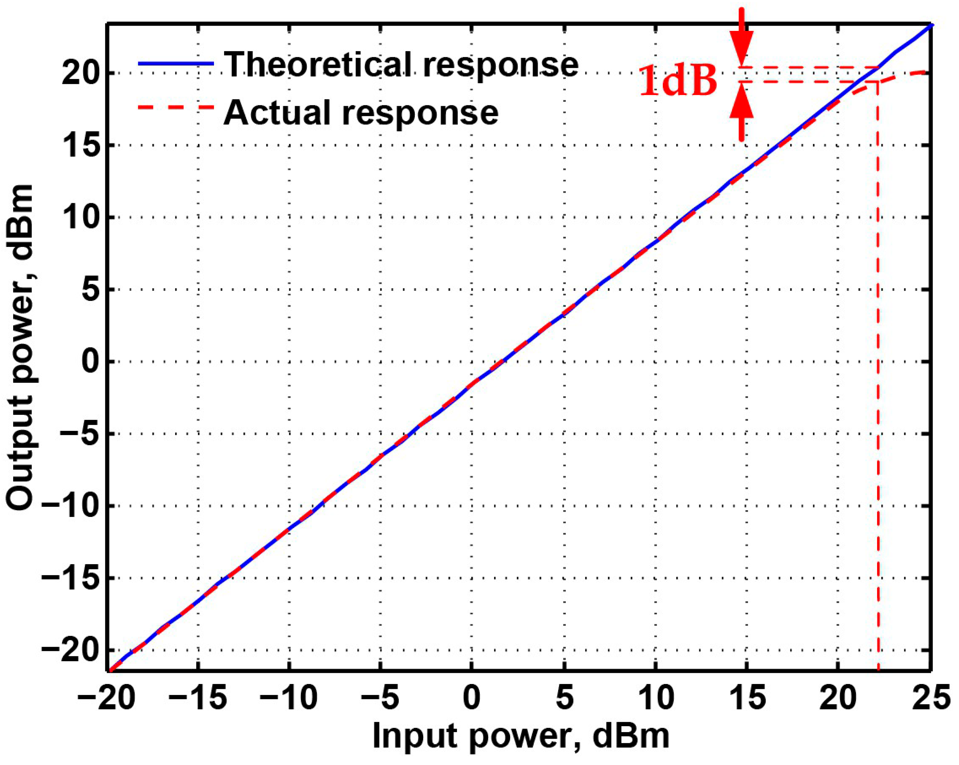
Measured the input one-dB power gain compression point (dBm)1222
Measured the third-order intermodulation distortion point (dBm)21.5933.84
Table 3. The linearity performance of P1dB and total power consumption with different input signal voltages.
Supply
(V)
Band-Pass Filter (Vo1) Low-Pass Filter (Vo2)Band-Reject Filter (Vo3)
Power (dBm)PD
(mW)
P1dB
(dBm)
Power (dBm)PD
(mW)
P1dB
(dBm)
Power(dBm)PD
(mW)
P1dB
(dBm)
InputOutputInputOutputInputOutput
±6−20−21.5626422−20−21.3826421−20−21.1926422
−10−11.53264−10−11.32264−10−11.15264
0−1.492640−1.262640−1.1264
108.46300108.67300109300
2018.163962018.153962018.72408
2118.914082118.794082119.42432
2219.464202219.254082219.82444
2319.84322319.474202320.11456
2420.024322419.584202420.33456
2520.244442519.654202520.52456
±9−20−21.639626.8−20−21.339626.1−20−21.2339626.3
−10−11.56396−10−11.26396−10−11.19396
0−1.53960−1.223960−1.12396
108.44450108.68450108.97450
2018.356662018.46662019.02684
2422.268462422.28462422.92864
2523.189002523.099002523.76918
2623.929362623.779362624.23972
26.824.297226.123.893626.324.3972
2724.289902724.119722724.51990
±12−20−21.5452828.5−20−21.2652827.7−20−21.1552827.5
−10−11.5528−10−11.23528−10−11.11528
0−1.465280−1.225280−1.06528
108.49600108.7600109.04600
2018.358882018.468882019.04912
2523.312242523.212242524.081272
2624.2613202624.0313202624.921368
2725.1214162725.114162725.351440
2825.8160827.725.58153627.525.51464
28.52616802825.715842825.721512
±15−20−21.4866028.8−20−21.1766028−20−21.863027.5
−10−11.36660−10−11.14660−10−11.04630
0−1.416900−1.16900−0.99660
108.53750108.82750109.1750
2018.4311102018.5711102019.111110
2523.3515602523.3415602523.981590
2624.3316802624.3616802624.631710
2725.1519202725.1618302725.41800
2825.920102825.8201027.525.71830
28.826.4216028.225.920402825.81890
Note: PD: Dynamic power consumption; P1dB: input one-dB power gain compression point.
Table 4. Phase noise performance measured at different oscillator frequencies.
Quadrature Output Voltage Vo1Quadrature Output Voltage Vo2
fo
(kHz)
Phase Noise
(dBc/Hz)
FoM
(dBc/Hz)
fo
(kHz)
Phase Noise
(dBc/Hz)
FoM
(dBc/Hz)
8.185.2398.58.187.6101.2
13.383.36103.913.384.35102.2
20.784.27105.720.780.59102.3
30.984.98110.030.984.61109.8
41.683.56111.241.681.87109.7
46.184.09112.446.184.39113.1
52.182.84112.452.182.66112.4
59.681.95112.759.683.29114.2
69.380.74112.869.381.76114.0
83.492.25126.583.482.21116.0
104.175.23110.8104.174.24110.0
13868.28120.813865.43103.6
205.862.26118.4205.876.57118.2
256.747.0990.3256.776.48120.1
300.575.29119.9300.571.3116.3
356.973.92119.9356.953.93100.4
402.773.54120.7402.772.43119.9
Note: fo: Oscillation frequency; and FoM: Figure-of-Merit.
Table 5. Phase noise performance measured at different supply voltages.
VDCOutput Voltage Vo1Output Voltage Vo2
Phase Noise
(dBc/Hz)
Δf
(Hz)
PDC
(mW)
fo
(kHz)
FoM
(dBc/Hz)
Phase Noise
(dBc/Hz)
Δf
(Hz)
PDC
(mW)
fo
(kHz)
FoM
(dBc/Hz)
±4.571.41100216102108.473.46100225102110.2
±672.26100300102107.874.24100300102109.8
±972.67100432102106.776.91100450102110.7
±1271.9100576102104.671.6100624102103.9
±1569.88100720102101.776.28100780102107.7
Note: VDC: Supply voltage; Δf: Offset frequency; PDC: Power consumption; fo: Oscillation frequency; and FoM: Figure-of-Merit.
Publisher’s Note: MDPI stays neutral with regard to jurisdictional claims in published maps and institutional affiliations.

