
Abstract
This paper demonstrates the first vertical field-effect transistor based on gallium nitride (GaN) fin structures with an inverted p-doped channel layer. A top-down hybrid etching approach combining inductively coupled plasma reactive ion etching and KOH-based wet etching was applied to fabricate regular fields of GaN fins with smooth a-plane sidewalls. The obtained morphologies are explained using a cavity step-flow model. A 3D processing scheme has been developed and evaluated via focussed ion beam cross-sections. The top-down approach allows the introduction of arbitrary doping profiles along the channel without regrowth, enabling the modulation of the channel properties and thus increasing the flexibility of the device concept. Here, a vertical npn-doping profile was used to achieve normally-off operation with an increased threshold voltage as high as 2.65 V. The p-doped region and the 3D gate wrapped around the sidewalls create a very narrow vertical electron channel close to the interface between dielectric and semiconductor, resulting in good electrostatic gate control, low leakage currents through the inner fin core and high sensitivity to the interface between GaN and gate oxide. Hydrodynamic transport simulations were carried out and show good agreement with the performed current–voltage and capacitance–voltage measurements. The simulation indicates a reduced channel mobility which we attribute to interface scattering being particularly relevant in narrow channels. We also demonstrate the existence of oxide and interface traps with an estimated sheet density of 3.2 × 1012 cm−2 related to the Al2O3 gate dielectric causing an increased subthreshold swing. Thus, improving the interface quality is essential to reach the full potential of the presented vertical 3D transistor concept.
Export citation and abstract BibTeX RIS

Original content from this work may be used under the terms of the Creative Commons Attribution 4.0 license. Any further distribution of this work must maintain attribution to the author(s) and the title of the work, journal citation and DOI.
1. Introduction
Gallium nitride (GaN) is a very promising candidate for future power electronics due to its wide band gap, high critical field strength and large electron mobility. Its superior material properties can lead to substantial efficiency improvement and size reduction with respect to silicon-based elements in switching applications. The first commercialized planar GaN high electron mobility transistors (HEMTs) demonstrated great performance for applications in the 650 V range, exploiting the excellent transport properties of the polarization field induced two-dimensional electron gas that is automatically formed at the polar GaN–AlGaN interface [1]. However, their lateral geometry imposes certain limitations such as limited breakdown voltage, natural normally-on characteristic as well as reliability issues. Vertical GaN transistor concepts such as CAVETs [2, 3] or trench MOSFETs [4] have been proposed and demonstrated impressive breakdown voltages of >1200 V, though such concepts usually rely on expensive bulk GaN material or even require several regrowth steps.
Here, we propose a vertical 3D architecture to merge additional advantages through the usage of GaN high aspect ratio nanostructures [5]. GaN nanostructures are expected to offer an optimized electrostatic control over the channel by 3D wrap-around gates [6], large nonpolar areas at their sidewalls suitable for normally-off operation, suppression of leakage currents through surface depletion in small diameter structures [7] and strain relaxation due to their small footprint [8]. Previously realized vertical GaN nanowire (NW) FETs have shown promising device performance [9–11]. However, the small footprint of NWs limits their mechanical stability and makes it challenging to upscale such devices to macroscopic currents by means of parallel integration. Therefore, more stable fin structures are explored in this work. The upscaling capability of vertical GaN fin FETs has been demonstrated in [12], where impressively high currents up to 5 A at 1.2 kV were achieved using expensive bulk GaN substrates.
In this work, metal-organic vapor phase epitaxy (MOVPE) grown GaN-on-sapphire wafers and conventional photolithography were used, exploring the suitability of the fabrication process for potential low-cost and mass production. Moreover, the fin dimensions can be precisely controlled via etching, and small widths far below the photolithography resolution limit down to 60 nm could be achieved. The top-down approach allows to define arbitrary vertical doping profiles during the epitaxial layer growth and hence enables the modulation of the channel properties. Here, an inverted p-doped channel layer is used to increase the threshold voltage as desired for safe power switching [1]. The channel current is carried by electrons.
2. Methods
2.1. Device fabrication
The device consists of vertically aligned fin structures with wrap-around gates controlling the vertical channel at their sidewalls. The GaN fins with non-polar a-plane sidewalls were obtained in a hybrid top-down etching approach.
Two types of GaN templates with slightly different layer configurations were grown by MOVPE on 2'' c-plane sapphire substrates. The GaN layer stack of type A wafers consists of 2 µm n-GaN buffer, 1.5 µm n+ -doped source access layer (ND = 1019 cm−3), 0.37 µm p-GaN channel layer (NA = 5 × 1017 cm−3), 2 µm unintentionally doped drift region (ND = 5 × 1016 cm−3) and 0.3 µm n+ -doped drain access layer (ND = 1019 cm−3). The p-doped region is inserted in order to increase the threshold voltage similar to previous work on NW FETs [10], which is desired for safe power switching. A second wafer type B with reduced doping concentration of the source access region (ND = 1018 cm−3) as well as slightly higher doping concentrations in the channel (NA = 1018 cm−3) and drift region (ND = 1017 cm−3) was used for wet etching studies.
The hybrid top-down etching approach is illustrated in figure 1. The GaN wafers were patterned with narrow Cr lines by conventional photolithography and lift-off techniques which served as etching mask for the following dry etching. Inductively coupled plasma reactive ion etching (ICP RIE) with SF6 and H2 was carried out forming 3.2 µm high tapered structures with rough surfaces (figure 1, left SEM image) suffering from ion bombardment damage, which can create leakage paths in electronic devices [13]. Thus, wet chemical etching with AZ400K developer (2.38% buffered KOH) at 90 °C was applied afterwards to remove the damaged surface, smoothen the sidewalls and further reduce the dimensions, resulting in fins with typically smooth vertical a-plane sidewalls (figure 1, right SEM image). The small etching rate of (38.8 ± 1.6) nm h−1 allows a precise control of the fin dimensions and small fin widths down to 60 nm could be achieved. The wet etching mechanism is discussed in more detail in section 3.
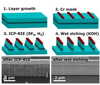
Figure 1. Fabrication of GaN fins via a hybrid top-down etching approach. The SEM images show the sidewall morphology of fins from wafer type B after ICP (left) and wet etching (right), which is used to remove the damaged surface, smoothen the a-plane sidewalls and reduce the fin dimensions.
Download figure:
Standard image High-resolution imageSeveral sequential processing steps were applied to fabricate FET devices as sketched in figure 2. After cleaning with Piranha solution and Cr etching, the Mg acceptors in the p-layer were activated via two-step rapid thermal annealing at 950 °C and 600 °C for 30 s and 300 s, respectively. The previous 3D structuring enables the successful activation of the buried p-doped layer through the fin sidewalls as verified by electron-beam induced current measurements at a cleaved fin cross-section (not shown here). Then, the fins were uniformly coated with a 25 nm thick high-quality Al2O3 gate dielectric by atomic layer deposition (ALD) at 200 °C using TMAl and water as precursors. An additional isolation layer of 200 nm SiOx was deposited within the fin spacings by e-beam evaporation, whereas shadowing from the mushroom-shaped top of the fins mostly prevented deposition on the sidewalls. The Cr gate metal was deposited on the sidewalls via tilted e-beam evaporation and subsequently formed into a 3D gate by filling the fin field with a photoresist, reducing the filling height with an ICP RIE O2 plasma treatment and etching away the Cr in the unprotected upper part of the sidewalls (see figure 2, step 3–6). After removal of the photoresist, a ~50 nm thick 3D gate metal remains at the sidewalls as shown in figure 2 step 6. The gate height can be controlled by the O2 plasma etch duration. In the presented finFET device, the gate reaches 1.3–1.6 µm above the p-doped region. An additional Al2O3 ALD step was conducted to prevent electrical shortcuts between gate and top electrodes. In a similar way to the gate formation, the oxides were removed from the fin tops. Finally, the fin array was planarized with a cured photoresist for mechanical support of the Cr/Au (70 nm/210 nm) top contact deposited by tilted e-beam evaporation.
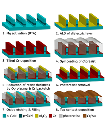
Figure 2. Sequential main 3D processing steps for the realization of vertical GaN finFETs. Steps 3–6 show the backetch approach for the 3D gate formation in detail. A similar procedure is used for both the oxide etching and the final filling in step 7. The additional isolation layer deposition after step 2 is not shown here.
Download figure:
Standard image High-resolution imageFigure 3 exhibits the fabricated finFET device consisting of 25 fins with a width of 400 nm and a spacing of 5 µm which were contacted over a length of 100 µm, yielding an active area of A= 0.01375 mm2 including the spacing between the fins. The different layers of a contacted fin can clearly be identified in the cross-section of the device prepared by ion milling with a focused ion beam (FIB) shown in figure 4, demonstrating the feasibility of complex 3D processing schemes in the GaN material system and the large degree of flexibility realized by the described 'technological construction kit'.

Figure 3. (a) Schematic sketch and (b), (c) 45° tilted SEM images of the fabricated vertical GaN finFET device consisting of 25 contacted fins.
Download figure:
Standard image High-resolution image
Figure 4. SEM image of a fin cross-section within a finFET device prepared by FIB with indication of the different materials. The Platinum layers above the bright Cr/Au top contact were deposited during the FIB preparation.
Download figure:
Standard image High-resolution image2.2. Simulation model
The carrier transport in the finFET devices has been modeled in detail with Synopsys Sentaurus to obtain more insight into the device physics. The physical modelling was mainly focussed on the stationary transfer characteristics as well as the small signal gate capacitance. Electrons are described by a hydrodynamic transport model, whereas holes are generally described by a drift/diffusion transport model. Details on the simulation model as well as the associated material parameters are given in a previous work [14]. The geometry of the simulation model was made to match the finFET geometry with tapered channel region shown in the FIB cross section in figure 4. The overlap of the gate electrode with the drift region (lgate) has been varied. The doping profile is identical to the type A layer stack outlined in the previous section. The dopant densities are considered as impurity densities subject to incomplete ionization. The electron mobility in the channel and drift region is subject to the doping concentration as well as Caughey-Thomas high-field saturation. Initially, the mobility/doping dependence according to Mnatsakanov et al [15] has been adopted. In absence of detailed reports on the electron mobility in p-GaN or near GaN semiconductor interfaces, the channel mobility has been used as a simulation parameter to match the transfer characteristics. The effect of oxide traps is modeled by traps at the GaN/Al2O3 interface that are equally distributed in the energy space. The ionization of the interface traps is subject to the Shockley model [16]. The trap density and distribution in energy space has been calibrated with the experimental subthreshold swing characteristics. Recombination is subject to Shockley-Read-Hall, radiative, and Auger processes. The nonlinear current versus voltage characteristic of the Cr/Au contacts has been investigated experimentally. The contact characteristic has been fitted with a barrier emission model to include it into the finFET simulation by means of a lumped circuit element in the source and drain path. In absence of a drain contact characterization the source and drain resistance are assumed to have the same characteristic in the simulation. The source contact resistance is more critical for the operation than the drain contact resistance because of its negative feedback on the gate-source voltage.
2.3. Characterization techniques
The devices were investigated in a Keithley model 4200 semiconductor characterization system by connecting Au plated probes to the source (S), drain (D) and gate (G) contact pads. The source was always connected to ground potential. In order to minimize possible self-heating effects, fast sweep rates of 0.54 V s−1 and 1.3 V s−1 were chosen for the drain and gate sweeps, respectively. Capacitance–voltage (CV) measurements were carried out with 30 mV AC amplitude at 50 kHz.
3. Wet etching study
Unlike for NWs, where the sidewalls evolve automatically according to the non-polar crystal plane with the highest etch rate, the sidewall orientation of fins is determined by the etch mask. Therefore, it is essential to align the Cr lines parallel to the preferential crystal plane revealed during etching in order to obtain smooth sidewalls. With the used AZ400K developer, fins with smooth a-plane sidewalls were obtained from lines extending along the m-direction, whereas fins along the a-direction showed rough m-plane sidewall morphologies with horizontal steps. It should be noted that the favored sidewall orientation depends on the etchant type and the concentration, e.g. wet etching with 1 M KOH or TMAH is reported to evolve smooth m-plane facets for both NWs [17] and fins [18]. These etchants were also tested here but the obtained m-plane sidewalls were rough and contained many horizontal steps. We therefore concentrated on fins etched by the first technique.
For the wet etching study, wafer type B with a lower doped n-GaN source access layer was used and processed into fins. The time evolution of the fin structures during wet etching is shown in figure 5. High semipolar etch rates cause the formation of vertical sidewalls already after 10 min of etching. Longer etching times of several hours slowly shrink the fin width further. Underneath the Cr etch mask, a concave mushroom-like etch undercut with chemically stable ( ) semipolar facets is evolving. An etch rate of (38.8 ± 1.6) nm h−1 was obtained from linearly fitting the width differences between the top and bottom of the fins over the etch duration (figure 5(b)). The lateral etch rate is more than a factor of 2 smaller compared to NWs under similar conditions [17], which is attributed to the concave geometry.

Figure 5. (a) SEM images of cleaved GaN fins show the time evolution during wet etching in KOH-based AZ400K developer at 90 °C. (b) Evaluation of the series yields an lateral etch rate of 38.8 ± 1.6 nm h−1 per sidewall.
Download figure:
Standard image High-resolution imageIn contrast to the smooth vertical a-plane sidewalls obtained from wafer type B, the fin structures from wafer type A used for the FET device exhibit a reversed bottleneck-shaped tapered fin base with a horizontal kink at the lower p-n junction as shown in the FIB cross-sections in figure 6. The different morphologies can be explained with the step-flow cavity etch model for GaN nanostructures introduced in [10], which is based on different step propagation velocities for the up- and downward movement of atomic scale cavity edges on a-plane GaN surfaces. The lower cavity creation rate νc for p-GaN compared to n-GaN is most likely caused by the different surface potential or the depletion of holes from the surface [10, 19]. It is a reasonable speculation that for the same reason, high n-doping concentrations enhance νc further, so that more cavities are generated at the bottom n+ -doped source access region than on the upper low-doped drift region. Due to the slow upward propagation, the additional cavity edges extend only slightly above the pn-junction and form a semipolar slanted sidewall composed of tiny horizontal steps that transitions into a vertical sidewall shaped by creation and fast downward movement of cavities from the upper n-GaN region.
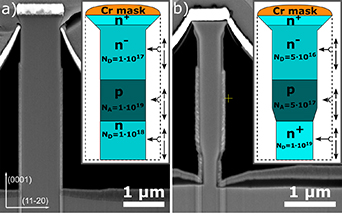
Figure 6. FIB cross-sections of GaN finFETs with (a) medium and (b) high n-doped source access layer at the bottom, corresponding to wafer type B and A respectively, show different sidewall morphologies after AZ400K wet etch at 90 °C. The insets sketch the kinetic step-flow cavity wet etch model of GaN fins as introduced in [10]. Atomic scale cavities are created on flat a-plane sidewalls with the rate νc, which propagate upwards and downwards with the velocities νs↑ and νs↓, respectively. The doping dependence of νc and the inhomogeneous step propagation νs↓ ≫ νs↑ explain the different fin morphologies.
Download figure:
Standard image High-resolution image4. Device characterization
4.1. DC characterization
The output (IDS-VDS) and transfer (IDS-VGS) characteristics of the finFET device are shown in figure 7. Within the measured range, a maximum current of 23 mA was obtained at VGS = 6 V and VDS = 3 V, corresponding to a current density of J= 174 A cm−2. An on-resistance of Ron = 17.5 mΩ cm2 is extracted from figure 7(a) at VDS = 2.38 V. It should be noted that the values could be easily further improved by reducing the dead space between the fins, for example by a factor of 2.2 for a reduction of the spacing to 2 µm. The device demonstrates normally-off operation with a threshold voltage of 2.65 V defined as VGS with maximum dgm/dVGS at low drain voltage VDS = 0.5 V according to the transconductance change method [20] as shown in figure 7(c). In our previous npn-NW FET with a similar design, a severe anticlockwise gate hysteresis was observed and attributed to the movement of mobile ions inside the SiO2 gate oxide [10]. Such gate memory effect could be suppressed in the finFET by using a more dense Al2O3 gate oxide instead which prevents the movement of mobile ions. No obvious gate hysteresis is visible in the bidirectional gate sweep (figure 7(b)). The maximal transconductance at VDS = 3 V (not shown here) is 83.9 mS cm−2. From the logarithmic IDS-VDS plot in figure 7(d), an on-off ratio of 109 is extracted. The very low gate leakage current of <35 pA proves the excellent insulation of the ALD oxide layer.

Figure 7. DC characteristics of the vertical GaN finFET: (a) drain sweep for different VGS, (b) bidirectional gate sweep with a sweep rate of 1.3 V s−1 for different VDS, (c) gate sweep and transconductance at VDS = 0.5 V and (d) switching characteristics and gate leakage at VDS = 3 V.
Download figure:
Standard image High-resolution imageSimulations of the transfer characteristics have been carried out for a nominal gate length lgate = 1.4 µm. With the channel mobility conforming to the mobility model [15] the simulated drain current is higher than in the experiment. Since the simulated capacitance shows very good agreement with the experiment (refer to section 4.4), the discrepancy can be attributed to the channel mobility. A good agreement of the transfer characteristic has been found for a channel mobility µn,ch = 5 cm2/(Vs) as shown in figure 8(a). This value appears to be quite low for electron transport in GaN, but there is strong evidence that the mobility in the p-doped channel is lower than predicted by the mobility model [21], similar to silicon MOSFETs. The inverted p-doped channel confines electrons close to the fin sidewall interface to the gate oxide and suppresses leakage currents through the inner part of the fin as reported for npn-NW FETs [14]. The inset in figure 8(b) shows the current density near the interface at different vertical positions. In the channel, more than 50% of the total current concentrates within 5 nm beneath the interface. The electron current in the channel is therefore subject to interface scattering, which is not included in the standard mobility model. The interface scattering might be enhanced by the occurrence of non-a-plane facets in the tapered channel region. For GaN/AlGaN HEMTs the effect of the interface roughness on the mobility has been discussed [22], but the situation here is quite different due to the interface to an amorphous oxide. Neutral impurity scattering at both active and inactive Mg sites in the p-GaN potentially contributes to the low electron mobility there.
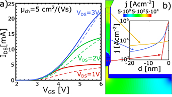
Figure 8. (a): Simulated transfer characteristic (solid lines) as a function of the drain voltage versus experiment (dashed lines). (b): current density distribution at VGS = 6 V, VDS = 3 V and current density in the channel and the drift region versus the lateral distance from the GaN interface towards the fin center.
Download figure:
Standard image High-resolution imageIt is noted that the drift region is not affected in the same way because the electron current is not as much confined to the GaN interface as in the channel region. The voltage drop in the drift region occurs between the end of the gate electrode and the highly doped drain region. Here, the current distribution is nearly uniform as shown in the inset of figure 8(b). Interface scattering has therefore only a minor influence and the low donor doping facilitates a high electron mobility.
The contact resistance further limits the drain current. Figure 9(a) illustrates the simulated transconductance characteristic without source and drain resistance. The transconductance shows saturation due to the influence of the drift region. The saturation as well as the maximum transconductance decrease with decreasing channel mobility. Figure 9(a) demonstrates that the contact resistance causes the strongest degradation, though. The linear decrease of the current and transconductance is caused by the mitigation of the gate electric field through the voltage drop in the source path. The drain resistance enhances the saturation of the transconductance. It also increases the absolute distance of the curves for VDS = 1 V, VDS = 2 V, VDS = 3 V in the transfer characteristic better matching the experimental data.

Figure 9. (a) Simulated transconductance at VDS = 3 V without (solid) and with source/drain resistance (dashed) for mobility model µch and µch = 5 cm2/(Vs). (b) Change of the simulated subthreshold transfer characteristic with the interface trap density (solid) compared to the experiment (dashed).
Download figure:
Standard image High-resolution image4.2. Subthreshold behaviour
The subthreshold behavior can best be analysed using the logarithmic IDS-VGS plot in figure 7(d). The rather large subthreshold swing of 282 mV dec−1 compared to previously obtained 67 mV dec−1 in NW FETs with similar methods [9] indicates the presence of interface or oxide traps which are filled during turn-on.
The trap density in the simulation has been calibrated with the experimental subthreshold characteristics. The interface or oxide traps have hardly any effect on the above threshold characteristic so that the subthreshold characteristic provides a means for estimating the trap density and distribution in energy space. Both the trap density and shape of the distribution matter. The nearly constant subthreshold swing in the experiment is indicating an equal distribution of traps in energy space.
Neglecting interface traps, the simulation would deliver a subthreshold swing of 75 mV dec−1. The experimental subthreshold swing of about 300 mV dec−1 can be obtained in the simulation with an interface trap density Nts = 3.2 × 1012cm−2 and an equal distribution of the trap levels ET within the first 0.36 eV below the conduction band edge  as shown in figure 9(b). This sheet density corresponds to an oxide trap density of at least Nox = 1.28 × 1018cm−3 assuming that all traps are evenly distributed inside the oxide. Al2O3 exhibits multiple native point defects and dangling bonds [23] which contribute to the energetic distribution of the traps as well as the potential gradient in the gate isolation. It is noted that there might be trap levels below the lower limit of the equal distribution, but these traps are not subject to the (de-)trapping, contributing a fixed charge, if any. They have hardly an effect on the subthreshold swing as well as the capacitance. The threshold has been matched varying the fraction of donor and acceptor traps. About 16% of the traps are acceptor traps, and 84% are donor traps. At VGS = 0 V virtually all donor traps are ionized enhancing the electron density. The acceptor traps remain neutral. With increasing gate voltage and thus decreasing distance of the electron quasi Fermi level, the donor traps become neutral whereas the acceptor traps are ionized carrying a negative charge. It is noted that the change of the charge with the Fermi level is the same for donor and acceptor traps, only the charge offset differs.
4.3. Breakdown voltage
Several devices were tested for breakdown voltage. In all devices, a destructive breakdown was observed between 67 V and 78 V (see figure 10). Simulations of the electric field distribution reveal that the peak of the field is located at the drain side of the gate across the dielectric layer, causing a dielectric breakdown. It should be noted that the device geometry is not optimized for high blocking voltages. Increasing the distance between gate and drain will allow much higher breakdown voltages, as a larger part of the potential difference drops in the depleted drift region. In [24], breakdown voltages above 650 V are predicted for NW FETs with a similar device structure, when choosing suitable doping and geometries that ensure depletion of the drift region.
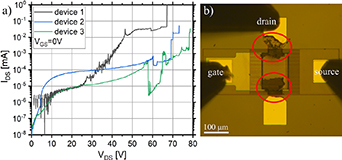
Figure 10. (a) Breakdown voltage measurement of three finFET devices at VGS = 0 V and (b) light-optical micrograph of a device after destructive breakdown.
Download figure:
Standard image High-resolution image4.4. Capacitance—voltage measurements
CV measurements with a DC voltage from −5–5 V and 30 mV AC amplitude at 50 kHz were carried out to further investigate the metal-oxide-semiconductor (MOS) interfaces and to check the oxide parameters used for the simulation. Due to different doping conditions and oxide thicknesses, the input capacitance Ciss= CGS+ CGD of the finFET consists of three parallel capacitances Cdrift, Cchannel and Csource as depicted in the geometric sketch in figure 11(a).

Figure 11. (a) Capacitive model of the finFET and (b) comparison of measured and simulated input capacitance Ciss= CGS+ CGD under consideration of different interface trap densities. The best agreement is reached for Nts = 1.6 × 1012 cm−2, indicating that not all traps can follow the fast AC modulation during the CV measurement at 50 kHz (black dashed line). The capacitance offset is attributed to the gate pad and supply line.
Download figure:
Standard image High-resolution image
The MOS capacitance has been simulated using the AC small signal model in Sentaurus Device for different trap concentrations. The results are depicted in figure 11(b) together with the experimental data. Experimental and simulated capacitance show a good agreement. The absolute difference of about 15 pF can be attributed to the gate pad and supply line capacitance Csrc,bottom. The overall good agreement of the simulated and experimental capacitance confirms the device dimensions and assumptions on the oxide permittivity.
The CV curve in figure 11(b) (black dashed line) rises at VGS= 0–1 V with the onset of electron accumulation in the drift region and again around VGS= 3 V when the channel is inverted. These two rising edges are also reflected in the simulation. The height of the increases illustrates that the largest contribution to the capacitance originates from the drift region. The obvious reason is the large overlap of the gate electrode there. The capacitance contributed by the channel is smaller.
The traps affect the capacitance in two ways. The static shift of the conduction band edge by the positive charge enhances the electron density near the oxide and thus the capacitance. Additionally, oxide and interface traps that can be charged sufficiently fast to follow the AC modulation affect the CV curve by dynamic (de-)trapping, and thus allow investigations of the trap dynamics in MOS structures, e.g. by the conductance method [25]. Therefore, the trap levels below the conduction band lead to a negative offset of the capacitance edge as shown in figure 11(b).
Deep traps in Al2O3 have been shown to interact on a timescale in the range of seconds [26]. The modulation frequency of 50 kHz is far beyond the transit frequency of the deep traps. Thus, these traps have no effect on the small signal capacitance. Therefore, the experimental capacitance does not reflect the effect of the oxide traps clearly, though it is suggested that there is contribution of traps with high transit frequency near VGS = 0 V.
5. Conclusion
In this work, we demonstrate the first vertical 3D GaN finFET with an inverted p-doped channel layer. Regularly arranged fin structures with a-plane sidewalls were fabricated in a top-down hybrid etching approach. The wet etching mechanism was studied further and the obtained fin morphologies were explained with the cavity step flow model. A 3D chip fabrication process has been developed to manufacture vertical finFET devices. Challenges of the 3D chip processing have been identified by a thorough FIB/SEM investigation. Hydrodynamic transport simulations were carried out and show good agreement with the performed DC and CV measurements. The usage of a p-doped GaN in the channel region allows the realization of normally-off devices with increased threshold voltages and confines the current flow to a very narrow channel close to the interface, which supports the electrostatic gate control and suppresses leakage currents through the inner part of the nanostructures. However, it also makes the device very sensitive to the interface conditions at the fin sidewalls, as expressed by the presence of oxide trapping and reduced channel mobility due to interface scattering observed in the presented fin devices. Thus, improving the interface quality is essential to reach the full potential of the presented device concept.
Acknowledgments
This work was funded by the Deutsche Forschungsgesellschaft (DFG, German Research Formation) within the project '3D Concepts for Gallium Nitride Electroncis'—284575374 and under Germany's Excellence Strategy—EXC-2123 Quantum Frontiers—390837967. The authors thank I. Manglano Clavero and C. Margenfeld for wafer growth in the Epitaxy Competence Center (ec2), a joint venture by the Institute of Semiconductor Technology and OSRAM Opto Semiconductors. We gratefully acknowledge the technical assistance of Juliane Breitfelder, Diana Herz and Angelika Schmidt.