Research on the Metasurface for Single-Photon Avalanche Photodiode
 Linyao Chen† Sunhao Zhang† Yuyang Ye† Chuang Liu† Tianqi Zhao* Yan Shi Ying Tian Rui Xu Yi Chen
- School of Optics and Electronic Technology, China Jiliang University, Hangzhou, China
As the core device of the quantum information field, the single photon avalanche photodiode (SPAD) is a solid-state single photon detector with a pico-second level time-resolution, low bias voltage, high signal-to-noise ratio, and a low cost. However, the photon detection efficiency (PDE) of SPAD is not ideal. The traditional method is to optimize the device structure, while the dark count or time resolution characteristics of the device might be sacrificed. The metasurface integrated on SPADs provides a novel approach to achieving higher PDE. As a result, the SPAD device structure could be independently designed to realize a low dark count rate and a good time resolution. In this paper, many kinds of metasurface structures that could enhance the incident photons absorption, are analyzed. Those structures compatible with CMOS or other easily mass produced processes are attractive for revolutionary changes to conventional SPAD. As a result, a metasurface integrated SPAD would greatly push its applications in the field of quantum information, single photons imaging, life medicine, and other low-level light detections.
Introduction
Quantum information technology is considered to be a key technology for the future. Quantum communication, quantum computing, and quantum measurement make up its main research directions [1–3]. In recent years, quantum information technology has greeted “the second revolution of quantum” and is accelerating from being experimental to real world application. Its potential in national security, national defense, economic development, and science technology is slowly emerging [4]. Along with the push of the rapid development of quantum information technology, the single photon avalanche photodiode (SPAD) as a core device is being taken more seriously by more people.
SPAD is a solid-state single photon detector with pico-second level time-resolution. After adding reverse bias on its p-n junction, the incident light will be absorbed and produce a light current. The reason this photodiode called SPAD is the phenomenon of a Geiger avalanche generation is because the reverse bias is beyond the breakdown voltage. Compared with regular PIN type photo diodes, the SPAD has extremely high responsiveness, and could resolve single photons. Furthermore, SPAD also has advantages in high signal-to-noise ratio, operation in the room temperature, and is cost effective. Thanks to these advantages, SPAD is extensively applied in medicine [5], quantum computing and measurement [6], molecular imaging [78], and other aspects, as shown in Figure 1.
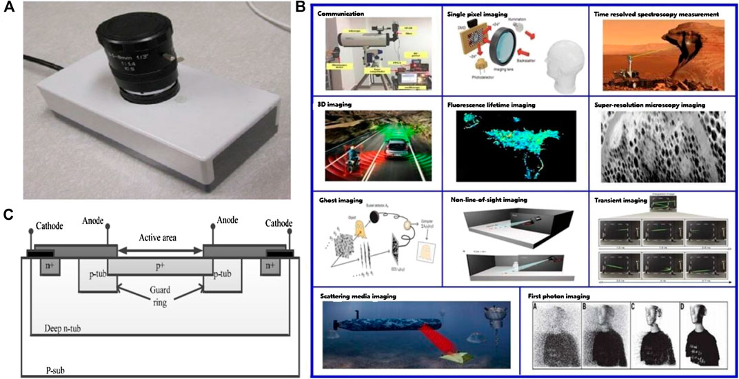
FIGURE 1. (A) Packaged SPAD optical imager. Source: Reproduced from Ref. 7. (B) applications of SPAD. (C) the Silicon-based SPAD structure diagram compatible with CMOS process. Source: Reproduced from Ref. 15.
However, the photon detection efficiency (PDE) of SPAD is not ideal. For example, the PDE of Silicon-based SPAD is not good in a near-infrared wavelength, which limits the detection performance in the application of LiDAR, etc. Recently, with the development of metasurface [9–12], the SPAD integrated with nano-structures (i.e., metasurface) was presented to overcome this drawback [13]. When this new SPAD accepted the perpendicular incidence of photons, some photons would change their direction in the nano-structure and the travel path in the absorbed layer of these photons was increased, which improves the PDE dramatically [14]. The resonant cavity to create an optical resonance in the vertical direction could also be used. Moreover, the SPAD integrated with the metasurface not only performs well in PDE, but also holds other SPAD performance metrics well, such as dark count rate, after the pulse, and time resolution [14]. The SPAD structure could be independently designed to realize a low dark count rate and a good time resolution without considering the effect of PDE on the device structure, therefore, the metasurface integration is a revolutionary technology for the development of SPAD, which would strongly push its applications in the quantum information fields.
Metasurface Structures and the Fabrication Methods
Many types of metasurface structures and corresponding fabrication methods are discussed below. Some metasurface are directly integrated on the bottom of the SPAD device. Some, used in solar cells and other fields, can be further applied to SPAD to improve its PDE.
Nano Pyramidal or Conical Array
The light-trapping SPAD is a typical mesa-type, shallow-junction SPAD fabricated using a complementary metal oxide semiconductor (CMOS) compatible process. Si epitaxial layers with a total thickness of 2.5 μm are grown on an SOI substrate. As shown in Figures 2A and 3, the nano-structure is etched as an inverse pyramid, with 850 nm period in a square lattice pattern. Unlike the resonance peaks found in the responsivity of resonant-cavity-enhanced (RCE) detectors, the light-trapping SPAD has broadband responsivity enhancement. The enhancement of external quantum efficiency (EQE) mainly comes from the anti-reflection effect of the nano-structures, and the contribution from nano-structure diffraction [13]. As shown in Figures 2 B and C, the enhancement effect of EQE is more obvious for the longer wavelength.
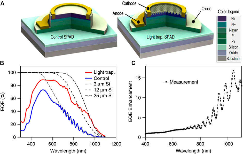
FIGURE 2. (A) Three-dimensional (3D) cross-sectional schematics of layer configurations of control (left) and light-trapping SPADs (right). (B) EQE measurements of control (blue solid) and light-trapping SPADs (red solid); dashed black lines correspond to theoretical absorption of 3, 12, and 25 μm thick Si from left to right. (C) EQE enhancement: ratio of light-trapping SPAD EQE compared to control SPAD. Source: Reproduced from Ref. 13.
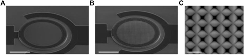
FIGURE 3. Structure of control SPAD (A) and light-trapping SPADs (B), both with 50 μm diameter. Scale bar in both 20 μm. (C) SEM image (top-down view) of inverse pyramid nano-structure on light-trapping SPAD. Scale bar, 1 μm. Source: Reproduced from Ref. 13.
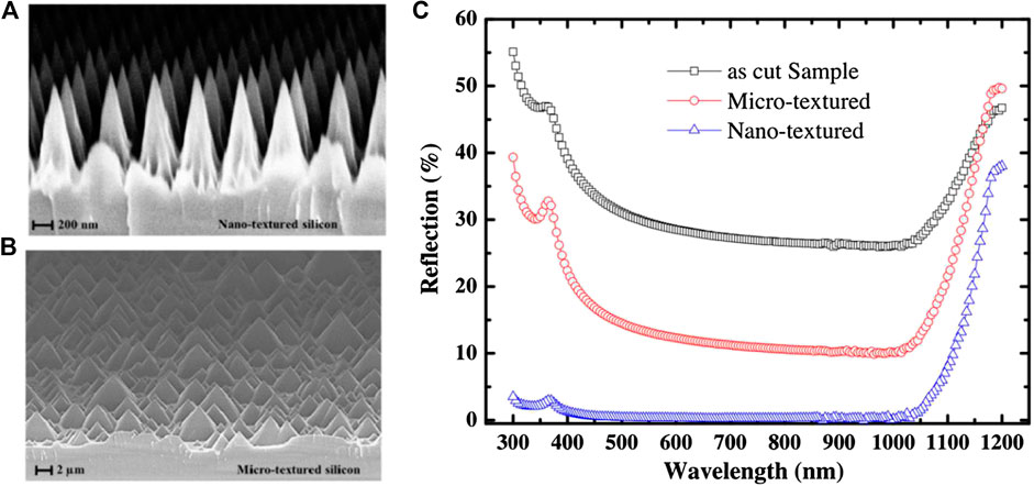
FIGURE 4. Image of nano-textured Silicon pyramids (A) and micro-textured Silicon pyramids (B). (C) Overview of hemispherical total reflectance measured on micro-, nanotextured and reference wafers. Nano-texture surface possesses excellent antireflective properties over a wide wavelength range. Source: Reproduced from Ref. 21.
Fabrication of anti-pyramid nanostructures [13]. First, a 2.5 µm Silicon layer is epitaxially grown on a SOI substrate. A reduced pressure chemical vapor deposition (CVD) is used to place 220 nm silicon on the oxide layer of 400 nm. Then, 200 nm of low temperature oxide (LTO) is deposited in a low-pressure chemical vapor deposition reactor at 400°C, a hard mask for etching nanostructures. The holes with square or hexagonal patterns were opened in the LTO mask layer by lithography and plasma using NF3 gas etching. The entire wafer is then immersed in tetramethylammonium hydroxide to wet etch silicon at 70°C and forms a 600 nm deep etch inverse pyramid which is a nanostructure. After surface texturing, different mesa diameters were designed to be plasma etched in HBr, Cl2, and O2 gas environments, then cleaned and thermal oxidation passivated at 1,000°C. After manufacturing, HF wet etching was used to open the holes, and 10 nm Ti and 200 nm Al were deposited as the readout electrode. This fabrication method has great commercial value, because it is compatible with CMOS process and obtains the potential of large-scale integration and low-cost applications.
The random vertical and inverted pyramids can increase light absorption by decreasing the broadband reflection, which scatters and captures incoming light efficiently, regardless of the angle of incidence photons [16–20]. The broadband reflection can be further reduced by using the nanotextures [21] as shown in Figure 4. This is because when the size of the nanostructure is smaller than the wavelength of the incident light, the optical coupling can be enhanced by the refractive index grading effect. Nanostructures are usually fabricated by wet chemical etching, dry etching, or a combination of photoetching and dry etching [22–25]. By combining the mixed micro/nano textures on the Silicon surface, the broadband reflection can be suppressed to less than 10%, even without the use of any additional anti-reflection coating on the mixed textures [26–28].
The nano cone array on the silicon as shown in Figure 5 can be made by self-assembled nanosphere lithography technology [29]. In the fabrication of arrays, different sizes of polystyrene sphere (PS) can adjust the period, the height and basal diameter of the nano cone array can be controlled by diverse etching time of the RIE procedure, and the deposition process can decide the thickness of the Au layer.
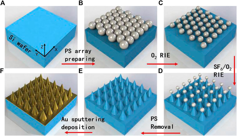
FIGURE 5. The fabrication of nano cone array with Au layer. Source: Reproduced from Ref. 29.
As shown in Figure 6A, this nano cone array structure (Figure 5E) can decrease optical reflection of the Si surface and increase absorption effectively in the visible spectrum. After the Au layer deposition on the Si nano cone array structure (Figure 5F), the high light absorption efficiency was significantly realized within the near infrared wavelength of 1,200–2,400 nm. This is because metallic nano-structure on the Silicon substrate causes surface plasma, which can enhance absorption and overcome the limitation of a silicon band gap. Moreover, the presence of the Au film can dramatically restrain reflection and transmission, resulting in a high absorption. This novel method is suitable for mass production and provides a way for infrared photon detection by Silicon-based SPAD.
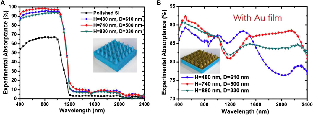
FIGURE 6. The absorption efficiency of nano cone arrays with or without Au layer. H and D is the height and diameter of the nano cone. Source: Reproduced from Ref. 29.
The two-dimensional periodic array of the nano pyramid was studied by Q. Han [30] as shown in Figure 7. The material of the pyramid is Ge. Through the nano pyramid array structure and various control methods, we would like to discuss the influence of thickness and height of the silicon substrate on absorption. As can be seen from Figure 7C, the average absorption rate improves with the increase of underlaying Si-layer thickness, which is compatible with SPAD with a chip thickness of several hundreds of microns. The nano pyramid array extends the optical path providing more Fabry-Perot resonances, which means that the absorption can be improved by increasing the nano pyramid height. As shown in Figure 7D, the efficiency of light absorption tends to be stable when the height is 0.9 μm.
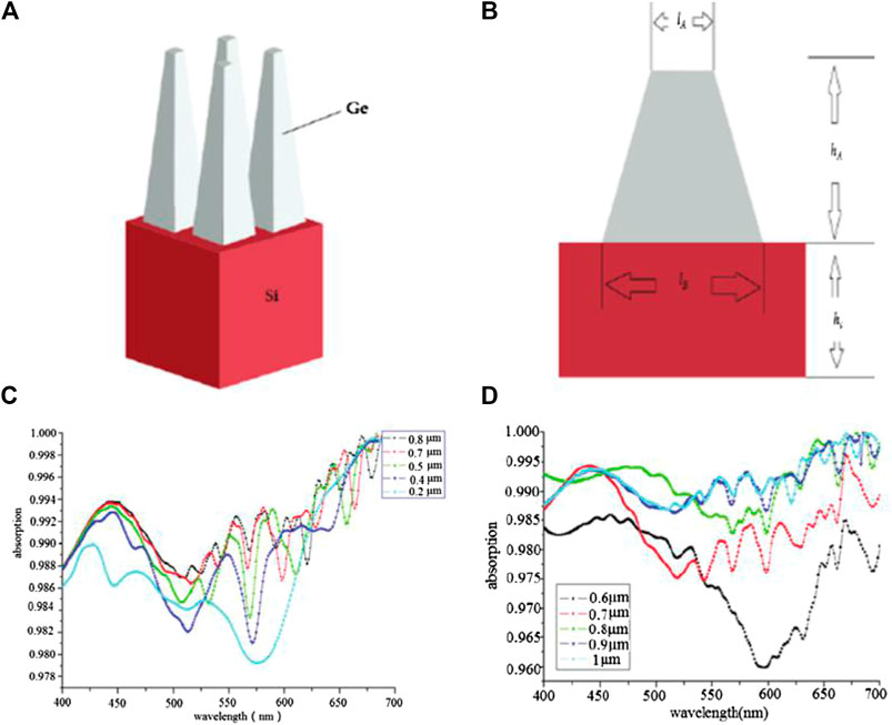
FIGURE 7. (A) Three-dimensional structure; (B) side view (C) Curve of absorbance with underlayment thickness, (D) The influence of the height of the quadrangle on the absorptivity. Source: Reproduced from Ref. 30.
Fabrication of the nano pyramid array [30]. A 1 μm thick germanium film was coated on the Silicon layer by electron beam evaporation. A focused ion beam instrument (FEI NOVA200 Nanolab) was used for the nanometer processing experiment, with a 30 KeV ion source with a tip current of 4pA–19.7 nA and an ion beam with a limiting pass-through aperture of 25 –350 μm. With the aid of a computer program, the intensity of the ion beam varies according to the milling depth. During milling, the ion beam and ion dose were 20 pA and 0.25nC/μm2, respectively. The working distance from the sample surface to the ionic cylinder is 20 mm. The electron mode of focused ion beam milling is selected to mill germanium films. After continuous milling, the square area of the pyramid structure is completed, as shown in Figure 8. Most traditional focused ion beam processing is two-dimensional. This three-dimensional processing is difficult and the operator's proficiency and operational experience requirements are high.
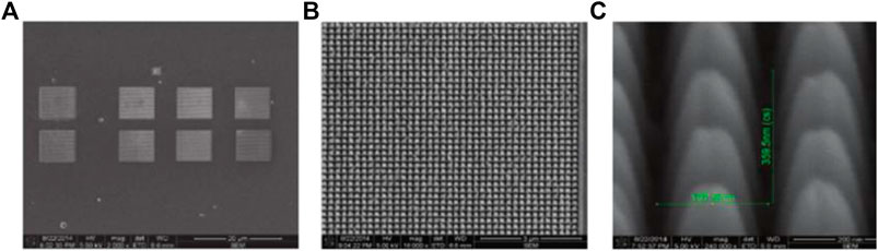
FIGURE 8. Under different magnification, the SEM image of the processed nanometer four-pyramid array is obtained. (A) in a 20 μm field of view; (B) at 3 μm: (C) at 200 nm. Source: Reproduced from Ref. 30.
Nanowire Arrays
Figure 9A shows the geometry of the nanowire array. The structure consists of a GaAs substrate and periodic axial p-i-n junction GaAs nanowires by gas-liquid-solid growth. As a simulation, the diameter of the nanowire (D) was set as 250 nm, the D/P determined by the minimum repetition unit period (P) and D was fixed at 0.5. The influence of height, D/P, and P on the light absorption performance of the nanowire arrays was explored [18]. As shown in Figures 9 B and C, when the nanowire height or D/P increases, the light absorption of the nanowire array gradually becomes stronger, the wave peak moves to the long wavelength, and the absorption spectrum is wider. From Figure 9D, we can see that the absorption peak moves to the long wavelength with the increase of the nanowire diameter.
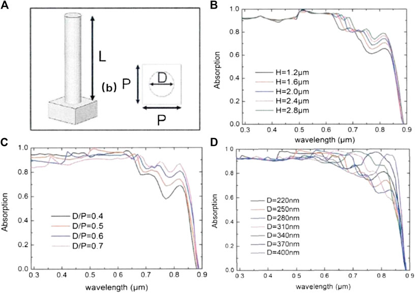
FIGURE 9. (A) Schematic diagram of minimum repeat unit in regular nanowire array, (B) Opticalabsorption performance of nanowire arrays with different heights, (C) Optical absorptivity performance at different D/P ratios, (D) Optical absorptivity performance of nanowires with different diameters. Source: Reproduced from Ref. 31.
Nanostructures could form on the Silicon surface from the bottom to the top using the self-assembly of silicon atoms [31]. Such methods include gas-liquid-solid growth, supercritical fluid growth, and oxidation catalysis growth. The growth principle of Si nanowires by gas-liquid-solid growth is shown in Figure 10. The growth of gas-liquid-solid mainly takes advantage of the catalytic effect of metal and combines it with gaseous reactants to grow silicon nanowires on the silicon surface. The Au particles deposited on the Si substrate react with the Si and Au-Si alloy droplets are formed at a certain temperature. As shown in Figure 10B, the eutectic point of the Au-Si alloy is greatly reduced. Si atoms are deposited on the substrate after SiCl4 and H2 are mixed. The Au-Si droplets continuously absorb Si atoms from the vapor so that the droplets maintain a supersaturation state. Since the melting point of Si (1,414°C) is far higher than the melting point of eutectic, Si atoms are precipitated out of the droplets and form a cylinder, and the droplets are lifted away from the substrate to form nanowires. Figure 10C shows the process of Si atom absorption, diffusion, and precipitation. Compared with the traditional gas-solid growth method, the advantage of the gas-liquid-solid growth method is that the activation energy required for growth is low, the nanowires grow only in the region where the catalyst exists, and the diameter is basically determined by the size of the Au catalyst. However, the biggest problem of nanowire arrays is that the periodic structures are difficult to fabricate accurately, which limits its real application.
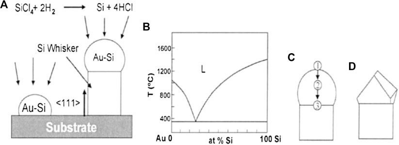
FIGURE 10. (A) Growth of whisker catalyzed by Au-Si liquid alloy formed on Si substrate, (B) phase diagram of Au-Si, (C) diffusion path of source reactant molecule through gold droplet, (D) growth of whisker catalyzed by solid catalyst. Source: Reproduced from Ref. 31.
Nano Spherical Structure
The aspect ratio (DW) of the concave array was simulated for the assessment of surface reflectivity [32]. Figure 11 shows the reflection curves of the structure with aspect ratios of 0, 0.2, 0.4, 0.6, 0.8, 1, and 2. The reflectivity decreases rapidly with the increase of the aspect ratio, and then tends to be smooth. Compared with the flat structure, the reflectivity of nano dimples or convex balls array structure is greatly reduced.
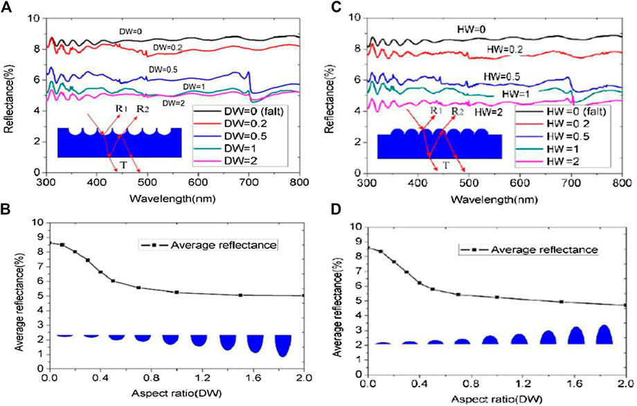
FIGURE 11. (A) The reflectance curves of nano dimples structure with DW of 0, 0.2, 0.5, 1, and 2 respectively, and corresponding average reflectivity (B). (C) The reflectance curves of nano convex balls structure with DW of 0, 0.2, 0.5, 1, and 2 respectively, and corresponding average reflectivity (D). Source: Reproduced from Ref. 32.
An example of convex balls array structure, the surface textured SPAD was proposed [33]. The schematic of epitaxial layer and surface textured SPAD and the fabricated results of SPAD and the surface nano-structure are shown in Figures 12A–C. The period of the convex balls array structure is 800 nm. Compared with the controlled SPAD (without convex balls array structure), the reflection measurement from the Si-air interface shows that the surface textured SPAD obtains higher light absorption efficiency (Figure 12D). PDE vs. the dark count rate plot in Figure 12E shows that there is an obvious increase of PDE for surface textured SPAD from 6.1 to 7.8%, which is a relative 28% added absorption over the control SPAD. This improvement is a contribution of the effects of anti-reflection and weak light trapping with photons scattered by the surface texturing structure.
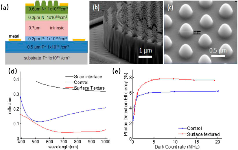
FIGURE 12. (A) Schematic of epitaxial layer and surface textured SPAD. (B) Fabricated SPAD. (C) Surface nano-structure. (D) Reflection measurement from Si-air interface, control SPAD mesa top and surface textured SPAD mesa top (E) PDE vs. DCR for both SPADs. Source: Reproduced from Ref. 33.
Fabrication of Si SPADs for surface texture [33]. First, epitaxial growth of a wafer takes place on a lightly boron doped substrate in a reduced-pressure chemical vapor deposition (RPCVD) system. As shown in Figures 12A–C, after the 2.3 μm oxide layer is grown, a thick contact layer is formed on the top. The 800 nm cycle photoresist was etched on the light etched column. The photoresist pillars refluxed and baked into a cone. Then the nano-cone pattern is transferred from photoresist to silicon, etched in CHF3 and O2 environments, passivated at high temperatures to form protective rings, and finally opened and deposited metal. This fabrication method is compatible with CMOS process and has a good business prospect.
An example of dimples balls array structure, random Silver nanostructures were formed on the top of the planar surface of Silicon, and the surface deformation of the nanostructures was carried out by the etching process [34], as shown in Figures 13A–C. A significant reduction in reflection can be obtained from the prepared silicon sample, with a reflection of about 2% over a wide spectral range between 300 and 1,050 nm (Figure 13D). The etching depth can be controlled between 100 nm and 10 µm by controlling the etching time. This feature is critical because accurate etching depth control is critical for photon detection absorptivity. This work demonstrates the potential of the etching process for manufacturing high-efficiency, low-cost Si-SPAD.
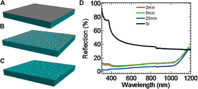
FIGURE 13. Schematic illustration of the fabrication process of nanostructured Si: (A) Silver film was deposited on the Si surface; (B) Silver nano-particles were formed after annealing silver film in a furnace; and (C) Si sample after etching in the HF and H2O2 solution. (D) Measured reflection spectra from nano-structured Si films with 9 nm silver film and different etching times. Source: Reproduced from Ref. 4.
Plasma resonance (SPR) as a regular technology, can be used to improve the absorption performance. Through the characteristics of SPR, reflection can be reduced, and light absorption can be promoted [35]. The structure of gold coated nanospheres is shown in Figures 14 A and B, which is formed by coating polystyrene microsphere array in hexagonal close arrangement. The bottom layer of the simulation model is a gold film. If the nanosphere array structure is coated with gold and filled with gold, the gold coated nanosphere shell array can be formed. In this model, the refractive index of the dielectric substrate is set to 1.43, i.e., The diameter of nanospheres is 630 nm. It can be seen from Figures 14 C and D, with the thicker coating thickness, the reflectance is lower, and the change is smaller. Under the thinner coating thickness, although there is a lower reflection trough, the wave the band width is too narrow. Therefore, the dependence of reflectance on different wavelengths gradually stabilizes, which is beneficial to a real fabrication process. For the detection of photons at specific wavelengths, the SPR nanosphere shell structure is a particluarly good choice.
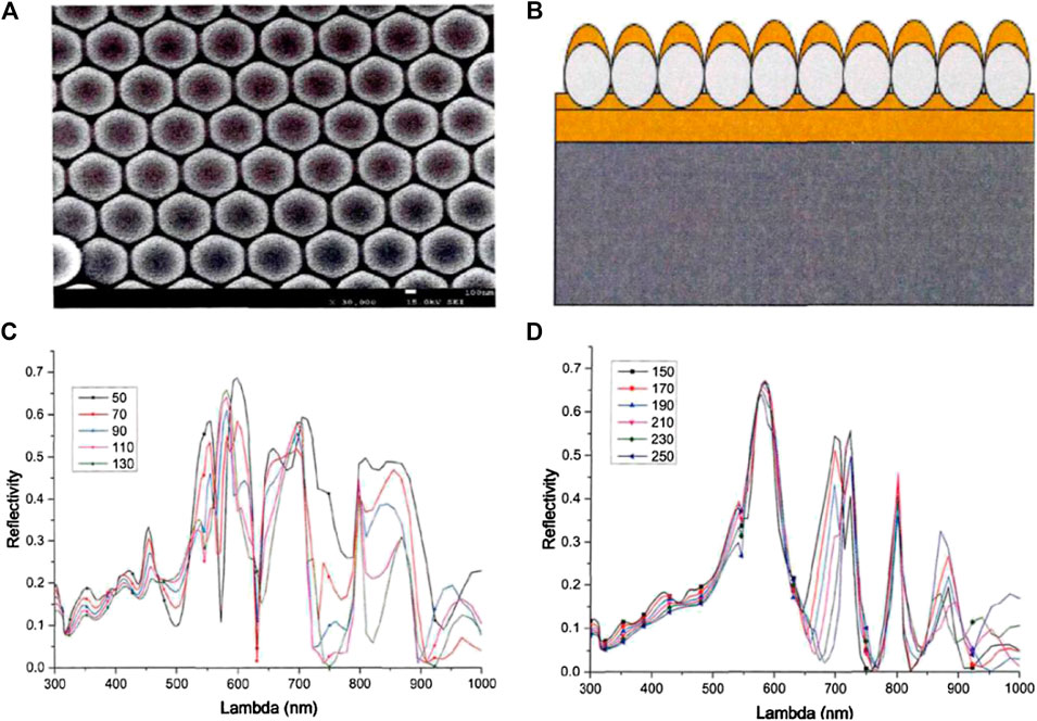
FIGURE 14. (A) It is the SEM picture of the nano spherical. (B) Schematic diagram of nanospheres. (C, D) The dependence of reflectivity on wavelength with different coating thickness. Source: Reproduced from Ref. 35.
The technological process of the fabrication of a nano-spherical shell structure [35]. As shown in Figure 15, a bottom layer of gold film is first evaporated on the substrate, then a single layer of hexagonal close-row microsphere film is formed on a silicon wafer through microsphere self-assembly technology, and the monolayer is transferred to the gold-plated substrate. Finally, the resistance evaporation film is applied again to form the structure of gold coated nanospheres.
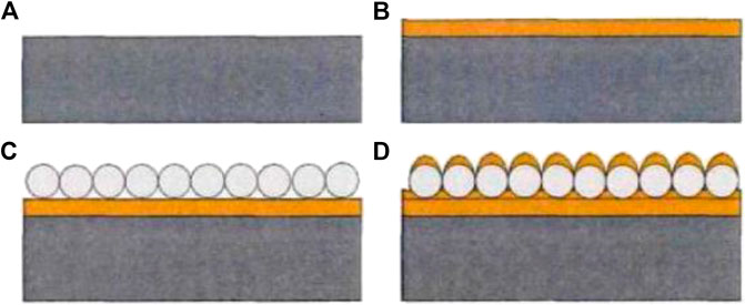
FIGURE 15. The technological process of fabrication of nano-spherical shell structure. Source: Reproduced from Ref. 35.
Deep-Trench Microstructures
The Silicon with a wide band gap of 1.12 eV is the key to the development of Silicon-based near infrared photodetectors. This results show that the microstructure can excite SPPs with wide frequency band and standing wave resonance of the plasma resonant cavity formed in the deep trench, thus producing a high frequency band and a high near infrared absorption in the range of 1,000–1,500 nm, as shown in Figure 16 [36]. It breaks through the absorption limit of Silicon and greatly expands its near-infrared absorption to 1,500 nm. When the groove becomes deeper, the absorption bandwidth and intensity of near-infrared absorption increases sharply. The microstructure makes it possible to achieve wide band and bloom response in the near infrared range from 1,000 to 1,500 nm.
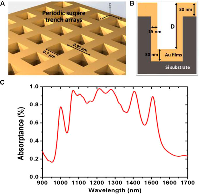
FIGURE 16. The deep-trench microstructures (A, B) and corresponding response in the near infrared range from 1000 to 1500 nm with D = 2.4 μm (C). Source: Reproduced from Ref. 36.
The optical properties of the SMART texture of crystalline Silicon was researched and optimized [37]. First, a pronounced nanotexture is imprinted into a high temperature stable silicon oxide (SiOx) sol-gel layer. Subsequently, the nanostructures are smoothed by spin-coating a titanium oxide (TiOx) sol-gel, which preferentially fills the void between the protrusions of the nanostructure. In the single-layer approach, a thin SiOx layer is sputtered on top of the smooth nanostructure. For the double-interlayer system, an additional silicon nitride (SiNx) layer is deposited prior to the SiOx layer. As a result, the absorption of the SMART texture structure is higher than that of the planar reference (Figure 17B).
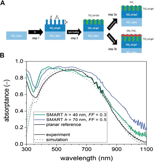
FIGURE 17. (A) the fabrication process of SMART texture of crystalline Silicon. (B) Comparison of absorption in 11 μm thick layers of silicon for two different nanostructures with lower (green) and higher (blue) filling fraction (FF) and height (h) as well as a planar reference interlayer stack (black). The experimental structures (solid) are compared to a 1-dimensional effective medium model with scattering model (dotted). Source: Reproduced from Ref. 37.
Prospect
Many kinds of metasurface structures that could improve incident photons absorption are analyzed in this paper. Structures that are compatible with CMOS or other easy to mass produce processes are attractive structures to be adopted to make revolutionary changes to conventional SPAD. As a result, the metasurface integrated SPAD would greatly push forward its applications in the quantum information, single photons imaging, life medicine, and other low-level light detections.
In ultraviolet band detection, the underspectral transfer can be carried out by preparing a spectral conversion layer on the SPAD surface, which will be a good research direction for SPAD to perform underspectral conversion. There are now some crystal materials that can carry rare earth ions for photoelectric conversion, such as YAG:Ce [38] and SrAl2O4 [3940]. YAG:Ce can absorb photons at short wavelengths, transform it into photons of long wavelengths, achieve the ultimate efficiency improvement in ultraviolet band detection. Similarly, in the near-infrared and infrared bands, rare earth ions can also absorb multiple long-wave radiation emitted by photons and convert them into short-wave radiation, a process known as upper-conversion luminescence. This material is of great significance in laser technology, optical fiber communication technology, fiber optic amplifier, and other fields [41]. At present, other researchers have also researched conversion materials [42–44].
Furthermore, the metamaterial could be used for multispectral imaging, by integrating it on the CMOS SPAD image sensor. Recently, an array of high-transmission mosaic filters was developed, each of which was completed by a single-step lithography process and was implemented by a plasmonic metasurface [45]. Integrated on the CMOS-SPAD array, the mosaic filter was reconstructed at the microphoto level of an average of five photons per pixel, and multispectral data at low-light levels was obtained simultaneously using three-color active laser lighting or broadband white light. This represents the first single-photon color image reconstruction achieved using a SPAD image sensor integrated with a mosaic filter array.
Author Contributions
TZ is the corresponding author of the article, who lead this scientific research work and wrote the paper. LC contributed to the study of the metasurface fabrication process. SZ contributed to the study of the metasurface structures. YY contributed to the study of the Introduction of the paper. CL contributed to the study of the prospect part of the paper. YS contributed partly to writing the introduction of the paper. RX contributed partly to writing about the nano conical array discussed in Nano Conical Array and the nanowire arrays discussed in Nanowire Arrays. YC contributed partly to writing about the nano spherical structure discussed in Nano Spherical Structure. YT contributed partly to writing the prospect part of the paper.
Funding
This work was supported by the National Key R&D Program of China (Grant No. 2018YFF0215304), the National Nature Science Foundation of China (NSFC) (Grant No. 61904169 and 61904168), the Zhejiang Provincial Natural Science Foundation of China (Grant No. LQ18F040001), the Technique Support Program of State Administration for Market Regulation (No. 2019YJ067), and the Major Scientific Research Project of Zhejiang Lab (2019DE0KF01).
Conflict of Interest
The authors declare that the research was conducted in the absence of any commercial or financial relationships that could be construed as a potential conflict of interest.
References
1. Han X, Feng L, Li Y, Zhang L, Song J, Zhang Y, et al. . Experimental observations of boundary conditions of continuous-time quantum walks. Chin Optic Lett. (2019). 17:052701. doi:10.3788/col201917.052701
2. Jung Lee H, Su Park H. Generation and measurement of arbitrary four-dimensional spatial entanglement between photons in multicore fibers. Photon Res. (2019). 7:19–27. doi:10.1364/prj.7.000019
3. Curic D, Giner L, Lundeen JS. High-dimension experimental tomography of a path-encoded photon quantum state. Photon Res. (2019). 7:A27–A35.
4. Tang C, Fang J, Wang L. Current status and future trends of quantum information technology. (2017).
6. Hadfield RH. Single-photon detectors for optical quantum information applications. Nat Photonics. (2009). 3(12):696–705. doi:10.1038/nphoton.2009.230
7. He W. Design of ultraviolet single photon counting imaging system based on avalanche photodiode. Nanjing: Southeast University (2018).
8. Ren M. Study on high-speed single-photon detection and applications.. Wuhan: Central China Normal University (2013).
9. Qiao J, Mei F, Ye Y. Single-photon emitters in van der Waals materials. Chin Optic Lett. (2019). 17:020011. doi:10.3788/col201917.020011
10. Ziaul Amin M, Mahbub Hossain M. Doping radius effects on an erbium-doped fiber amplifier. Chin Optic Lett. (2019). 17:010602. doi:10.3788/col201917.010602
11. Rusby DR, Armstrong CD, Scott GG, et al. Effect of rear surface fields on hot, refluxing and escaping electron populations via numerical simulations. High Power Laser Sci Eng. (2019). 7(3):e45. doi:10.1017/hpl.2019.34
12. Pan KQ, Yang D, Guo L. Enhancement of the surface emission at the fundamental frequency and the transmitted high-order harmonics by pre-structured targets. High Power Laser Sci Eng. 7(2):e36. doi:10.1017/hpl.2019.20
13. Zang K, Jiang X, Huo Y. Silicon single-photon avalanche diodes with nano-structured light trapping. Nat Commun. (2017). 8(1):22–27. doi:10.1038/s41467-017-00733-y
14. Jian M. Design of single photon avalanche diodes. Beijing: University of Science and Technology of China (2016).
15. Peng Y. Analysis and design of a single photon avalanche diode.. Xiangtan: Xiangtan University (2019).
16. Liu X, Coxon PR, Peters M, Hoex B, Cole JM, Fray DJ. Black silicon: fabrication methods, properties and solar energy applications. Energy Environ Sci. (2014). 7:3223–63. doi:10.1039/c4ee01152j
17. Liu R, Zhang F, Con C, Cui B, Sun B. Lithography-free fabrication of silicon nanowire and nanohole arrays by metal-assisted chemical etching. Nanoscale Res Lett. (2013). 8:155. doi:10.1149/ma2010-02/18/1315
18. Han H, Huang Z, Lee W. Metal-assisted chemical etching of silicon and nanotechnology applications. Nano Today. (2014). 9:271–304. doi:10.1117/12.2238480.5163995439001
19. Fan Y, Han P, Liang P, Xing Y, Ye Z, Hu S, Differences in etching characteristics of TMAH and KOH on preparing inverted pyramids for silicon solar cells, Appl Surf Sci. (2013). 264:761–6. doi:10.1016/j.apsusc.2012.10.117
20. Campbell P, Green MA. Light trapping properties of pyramidally textured surfaces. J Appl Phys. (1987). 62:243–9. doi:10.1063/1.339189
21. Khandelwal R, Plachetka U, Min B, et al. A comparative study based on optical and electrical performance of micro- and nano-textured surfaces for silicon solar cells. Microelectron Eng., (2013). 111:220–3. doi:10.1016/j.mee.2013.03.162
22. Noor NAM, Mohamad SK, Hamil SS, Devarajan M, Pakhuruddin MZ. Effects of etching time towards broadband absorption enhancement in black silicon fabricated by silver-assisted chemical etching. Optik. (2019). 176:586–92. doi:10.1016/j.ijleo.2018.09.096
23. Rahman T, Boden SA. Optical modeling of black silicon for solar cells using effective index techniques. IEEE J. Photovolt. (2017). 7:1556–62. doi:10.1109/jphotov.2017.2748900
24. Huang Z, Geyer N, Werner P, De Boor J, Gösele U. Metal-assisted chemical etching of silicon: a review. Adv Mater. (2011). 23:285–308. doi:10.1117/12.2238480.5163995439001
25. Pakhuruddin MZ, Dore J, Huang J, Varlamov S. Effects of front and rear texturing on absorption enhancement in laser-crystallized silicon thin-films on glass. Jpn J Appl Phys. (2015). 54:13–27. doi:10.7567/jjap.54.08kb04
26. Ingenito A, Isabella O, Zeman M. Nano‐cones on micro‐pyramids: modulated surface textures for maximal spectral response and high‐efficiency solar cells. Prog Photovolt Res Appl. (2019). 23:1649–59. doi:10.1002/pip.2606
27. Toor F, Page MR, Branz HM, Yuan HC. 17.1%-Efficient multi-scale-textured black silicon solar cells without dielectric antireflection coating. Conf Rec IEEE Photovolt Spec Conf. (2011). 12:20–4. doi:10.1109/pvsc.2011.6185835
28. Dimitrov DZ, Du CH. Crystalline silicon solar cells with micro/nano texture. Appl Surf Sci. (2013). 266:1–4. doi:10.1016/j.apsusc.2012.10.08
29. Li Q, Gao J, Li Z. Absorption enhancement in nanostructured silicon fabricated by self-assembled nanosphere lithography. Opt Mater. (2017). 70:165–70. doi:10.1016/j.optmat.2017.05.036
30. Qi H. Study of nanophotonic structures based perfect absorbers.. Beijing: University of Electronic Science and Technology of China (2015).
31. Gong L. The research on irregular nanowire array solar cells.. Beijing: Beijing University of Posts and Telecommunications (2016).
32. Chen L. Studies on enhancement efficiency of thin film silicon solar cells with high-efficiency surface light-trapping structure.. Shangai: Shanghai Jiao Tong University (2017).
33. Zang K, Ding X, Jiang X. Surface textured silicon single-photon avalanche diode. In: Proceedings of CLEO: Science Innovation. (2017).
34. Li R, Wang S, Chuwongin S. Nanoscale silver-assisted wet etching of crystalline silicon for anti-reflection surface textures. J Nanosci Nanotechnol. (2013). 13:493–7. doi:10.1166/jnn.2013.6916
35. Chen Y. Research on optimal design and application of perfect absorber based on surface plasmon resonance.. Wuhan: China Academy of Engineering Physics (2018).
36. Yang H, Liu X, Gao J. An extending broadband near-infrared absorption of Si-based deep-trench microstructures. Optic Commun. (2017). 392:59–63. doi:10.1016/j.optcom.2017.01.041
37. Eisenhauer D, Jäger K, Köppel G, Rech B, Becker C. Optical properties of smooth anti-reflective three-dimensional textures for silicon thin-film solar cells. Energy Proc. (2016). 102:121–134. doi:10.1016/j.egypro.2016.11.314
38. Shao G. Investigation on the enhancement of conversion efficiency of solar cell.. Nanjing: Southeast University (2016).
39. Nazarov M, Brik MG, Spassky D. Structural and electronic properties of SrAl2O4:Eu2+ from density fonctional theory calculations. J Alloys Compd. (2013). 573(10):6–10. doi:10.1016/j.jallcom.2013.04.004
41. Sanderson KD, Mills A, Parkin I. The use of titanium dioxide coatings deposited by APCVD on glass substrates to provide a dual action self-cleaning. In: 46th Annual society of vacuum coaters technical conference, San Francisco, United States (2003). 203–8.
42. Yu J, Zhao X, Lin L. Preparation and characterization of super-hydrophilic TiO2/SiO2 composite thin films. J Inorg Mater. (2001). 16(3):529–44. doi:10.1016/s0254-0584(00)00364-3
43. Zywitzki O, Modes T, Sahm H. Structure and properties of cry stalline titanium oxide layers deposited by reactive pulsemagnetr on sputtering. Surf Coat Technol. (2004). 180–181(3):538–43. doi:10.1016/j.surfcoat.2003.10.115
44. Wang H, Wang J, Wang H, Yang F. An anti-fog self-cleaning glass and preparation method. CN200610019338 (2004).
45. Shah YD, Connolly PWR. Ultralow-light-level color image reconstruction using high-efficiency plasmonic metasurface mosaic filters. Optica. (2020). 7(6):632. doi:10.1364/optica.389905
Keywords: metasurface, single photon detection, SPAD, metamaterial, PDE
Citation: Chen L, Zhang S, Ye Y, Liu C, Zhao T, Shi Y, Tian Y, Xu R and Chen Y (2020) Research on the Metasurface for Single-Photon Avalanche Photodiode. Front. Phys. 8:585871. doi: 10.3389/fphy.2020.585871
Received: 21 July 2020; Accepted: 28 September 2020;
Published: 16 November 2020.
Edited by:
Chee Leong Tan, University of Malaya,MalaysiaCopyright © 2020 Zhao, Chen, Zhang, Ye, Liu, Shi, Tian, Xu and Chen. This is an open-access article distributed under the terms of the Creative Commons Attribution License (CC BY). The use, distribution or reproduction in other forums is permitted, provided the original author(s) and the copyright owner(s) are credited and that the original publication in this journal is cited, in accordance with accepted academic practice. No use, distribution or reproduction is permitted which does not comply with these terms.
Correspondence: Tianqi Zhao, 18a0402151@cjlu.edu.cn
†These authors contributed equally to this work.