A Low-Temperature Solution-Process High-k Dielectric for High-Performance Flexible Organic Field-Effect Transistors
 Qi Mu1,2
  Shuming Duan
 Xiaotao Zhang
 Xiaochen Ren
- 1Tianjin Key Laboratory of Molecular Optoelectronic Sciences, Department of Chemistry, School of Science, Tianjin University and Collaborative Innovation Center of Chemical Science and Engineering (Tianjin), Tianjin, China
- 2School of Microelectronics, Tianjin University, Tianjin, China
- 3State Key Laboratory of Photocatalysis on Energy and Environment, College of Chemistry, Fuzhou University, Fuzhou, China
Applying high-k dielectrics can effectively reduce the operating voltage of Organic field-effect transistors (OFETs) to a few volts, thus significantly miniaturizing the dynamic power consumption of OFETs. Aluminum oxide is a promising dielectric material due to its high permittivity (k = 6–9). In this work, a simple, low-cost, low-temperature (only 85°C) solution process is used to prepare amorphous AlOx dielectric thin films for high-performance flexible OFET applications. The AlOx thin film was spin-coated and then solidified using deep ultraviolet irradiation without high-temperature annealing. The as-deposited AlOx thin film has a root mean square surface roughness of 0.47 nm and maintains a very low leakage current density of 8 × 10⁻⁹ A/cm2 at 3.5 MV/cm and high dielectric constant of about 8.3 (at 1 kHz). The complete OFET based on this dielectric can operate at a 3 V gate bias with saturation mobility of 1.8 cm2/Vs, and steep sub-threshold swing of 110 mV/dec. Our work demonstrated a low-temperature solution process to fabricate a high-k metal oxide dielectric for low-power OFET applications.
Introduction
Organic field-effect transistors (OFETs) have rapidly developed over the past decade and have shown superior device performances to amorphous Si transistors (Diao et al., 2013; Wang et al., 2013; Yamamura et al., 2018; Duan et al., 2020). OFET is known as the basic unit of organic integrated circuits and such devices are usually in array form in practical applications. The heat dissipation and power consumption of OFETs must be considered, particularly for a higher level of integration (Ren et al., 2018; Jiang et al., 2019). For OFET, the dynamic power consumption (Pdyn) is proportional to the square of the saturation gate voltage, so low-voltage OFETs can effectively reduce power dissipation in the whole circuit. Increasing the unit-area capacitance (Ci) is the key to reaching the low-voltage operation of OFET and Ci is determined by the relative permittivity (k) of the dielectric material and dielectric layer thickness. For commonly used SiO2 dielectrics with k = 3.9, one can reduce the dielectric thickness to increase the Ci until it reaches a few nanometers; further thinning the dielectric layer will result in a significant tunneling current and disable the device. Applying a high-permittivity (high-k) dielectric material allows the achievement of large unit-area capacitance with reasonable thickness that could largely reduce the operating voltage of OFETs while at the same time suppressing the tunneling current. While many high-k materials have been reported for OFET applications, such as AlOx, HfOx, ZrOx, and BST (Wang et al., 2014; Park et al., 2015; Sung et al., 2015; Park et al., 2017; Xia et al., 2018; Yang et al., 2018; Mullapudi et al., 2019; Wang et al., 2019), most of them require vacuum deposition or solution processing at a high annealing temperature.
Among different material deposition methods, the solution processing of high-k dielectrics by the sol-gel method is promising for its low-cost, being vacuum-free, and compatibility with industrial processing technologies such as spin coating, dip coating, inkjet printing, and roll-to-roll fabrication (Quah et al., 2010; Wang et al., 2013; Wang et al., 2014; Park et al., 2015; McKerricher et al., 2017; Quah et al., 2017; Heo et al., 2018; Jo et al., 2018; Xia et al., 2018; Bolot et al., 2019; Sun et al., 2019). In addition, the solution formed a densely packed thin film with atomic flat-surface roughness, thus facilitating good charge transport in organic semiconductors when deposited onto the dielectric layer, leading to high carrier mobility and low leakage current. To solidify the metal-oxide thin film and remove residual solvent/byproducts, the sol-gel method involves a high-temperature (200–400 °C) annealing process above the glass transition temperature of most flexible substrates; this hinders its application in flexible electronics (Park et al., 2020). Several attempts have demonstrated a reduction in the processing temperature of the sol-gel method, including deep ultraviolet (DUV) photochemical reactions or microwave-assisted solidification, for which the processing temperature is higher than 150°C (Park et al., 2015; Wang et al., 2019; Xia and Wang, 2019). Park et al. reported a detailed study of the rapid densification of metal-oxide thin films by DUV irradiation. DUV-induced photochemical activation largely reduces the processing time down to a few minutes but the annealing temperature of 150°C is still relatively high, meaning that it cannot be used for certain common flexible substrates such as PEN and PET (Hussain et al., 2020). Development of a solution-processed, low-temperature, and robust high-k dielectric thin film is urgently required to realize low-cost, flexible, and high-performance OFET devices.
In this work, we demonstrated a simple, low-cost, low-temperature (only 85°C) DUV solution process to prepare amorphous AlOx high-k dielectric thin films for high-performance OFET applications. The DUV-treated AlOx dielectric layer has a dielectric constant of about 8.3 (at 1 kHz) and a low leakage current density of 8 × 10⁻⁹ A/cm2 at 3.5 MV/cm. The complete OFET device is fabricated by the thermal evaporation of 2,9-didecyldinaphtho[2,3-b:2′,3′-f]thieno [3,2-b]thiophene (C10-DNTT) and Au top electrodes on both silicon and flexible substrates. The operating voltage of OFET is <3 V, with a saturation mobility of 1.8 cm2/Vs and negligible hysteresis. The low-temperature solution-processed high-k metal oxide dielectric has demonstrated its potential for low-power flexible transistors or capacitor applications and is ready for further scaling up and continuous production line fabrication (Figure 1).
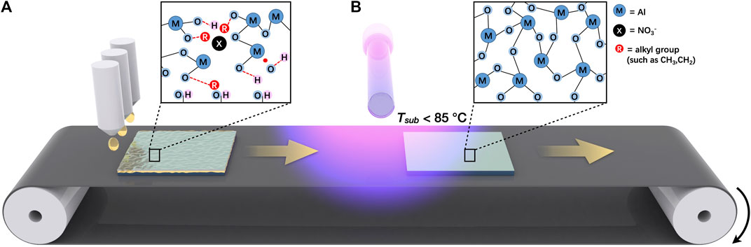
FIGURE 1. Schematic diagram of fabrication procedure of sol-gel AlOx dielectric thin film, in which (A) represents the solution deposition of the metal oxide precursor, and (B) represents the deep-UV photochemical activation process to solidify the thin film. Both the processes are compatible to large-scale, continuous production.
Experimental Section
Preparation of AlOx Thin Film
To prepare the sol precursor, 187–375 mg of aluminum nitrate nonahydrate (Al(NO3)39H2O) was dissolved in 5 ml of 2-methoxyethanol solvent. Next, the solution was vigorously stirred for>12 h at 75°C. Before deposition, the solution had been stored for 30 min at room temperature.
To prepare the AlOx thin film, the heavily n-doped Si wafer (resistivity 0.05–0.2 Ω·cm) with thermally grown 300 nm SiO2 (bought from China Electronics Technology Group Corporation) and PEN (Goodfellow, 125 μm thick) were used as substrates. The SiO2/Si and PEN substrates were cleaned by sonication in deionized water, acetone, and isopropanol for 5 min each and then blown dry using N2 gas flow. The AlOx sol precursor was spin-coated on SiO2/Si and PEN substrates with a 50 nm evaporated Au bottom electrode. The transparent precursor solution was filtered using a 0.2 μm polytetrafluoroethylene syringe filter to remove impurities and undissolved particles before spin-coating. The spin-coating rotation speed was 4,000 rpm for 30 s. To solidify the AlOx thin film, the as-deposited precursor film was irradiated under a high-density ultraviolet light for 80 min using a low-pressure Hg lamp (the emission wavelength was 90% 253.7 nm and 10% 184.9 nm, with light intensity of 65.5 mW/cm2 at 253 nm). UV light irradiation was performed inside an N2 glove box with oxygen concentration <1 ppm. The maximum local temperature at the substrate during UV light irradiation was 85°C, measured by a thermocouple. The control sample was annealed at 400°C in a furnace for an hour without UV exposure.
Fabrication of Organic Field-Effect Transistors
The OFET devices were fabricated by 40 nm of thermally-evaporated 2,9-didecyldinaphtho[2,3-b:2′,3′-f]thieno[3,2-b]thiophene (C10-DNTT) on top of the AlOx thin film along with the 30 nm Au top electrodes through shadow masks. The channel length (L) and width (W) were fixed at 30 and 70 μm, respectively.
Characterizations
The X-ray diffraction (XRD) results were obtained using a Rigaku SmartLab X-ray diffractometer with highest power of 9 kW (step size 0.01°). The atomic force microscope (AFM) images were obtained in Intelligent-mode using a Bruker Dimension Icon in air. For leakage and capacitance characterization, a metal–insulator–metal (MIM) structure was fabricated by depositing 50 nm Au electrodes onto the dielectric layer through a shadow mask. The frequency dependence of the capacitance and leakage current of the dielectric were measured by the Keithley 4200 SCS semiconductor parameter analyzer in air.
Results and Discussion
Figure 1 demonstrates the schematic drawing of the fabrication procedures, which can be summarized as solution-based deposition and optical solidification of thin film. The solution-processable characteristic and its simple light-triggered photoactivation indicates that it has high compatibility with industrial-scale continuous processes. As shown in Figure 1A, the as-deposited wet thin film must go through metal–oxygen–metal (M-O-M) bond formation, evaporation of metal ligands, solvents, and byproducts, and void densification to form densely packed, solid-state AlOx thin film. All the above-mentioned processes were completed with DUV irradiation for 80 min. In this process, the sample’s temperature was increased up to 85°C by heating with a Hg lamp and no external heat source was applied during the experiment. The mechanism of DUV irradiation has been widely investigated (Wang et al., 2013; Park et al., 2015); main peaks from the Hg lamp are produced at 184.9 nm (10%) and 253.7 nm (90%) and will be absorbed by the metal-oxide precursors, resulting in their decomposition into active oxide layers. We performed the DUV irradiation in an N2 gas-filled glove box with an oxygen concentration of <1 ppm so that no ozone could form during the process, thus ensuring that the efficient photochemical reaction was triggered by DUV light.
To verify the dielectric thin film quality, we characterized the thin film formed by DUV light irradiation and high-temperature annealing at 400°C as a control sample using attenuated total reflectance Fourier transform infrared, XRD, and an AFM. In Figure 2A, the ATR-FT-IR spectra of the DUV-treated sample indicates that the intensities of the broad IR absorption bands at 3,500 and 1,650 cm−1, which correspond to O-H stretching and H-O-H bending, respectively, are rapidly decreasing compared to the as-spun sample, close to the levels of the sample annealed at 400°C. In addition, the absorption bands at 1,400 and 1,340 cm−1—known as the N-O stretching modes in nitrate ligand—also disappear for the DUV sample. These results clearly prove that DUV photochemical activation effectively reduces the surface O-H functional group density and removes nitrate ligands within 80 min. In Figure 2B, the XRD pattern of the AlOx film, obtained by annealing at the high temperature of 400°C and DUV 80 min, are almost the same; there is no obvious diffraction peak for either sample, so the thin films are amorphous. For dielectric application, the amorphous structure is preferred because the presence of a crystalline structure or grain boundaries may become an alternate leakage current path or increase the surface roughness (Xia et al., 2018). Next, the surface mophology of AlOx thin film is characterized by AFM. Compared to the bottom Au electrode, for which the root-mean-square surface roughness (Rrms) is estimated to be 1.40 nm (Figure 2C), the AlOx thin film deposited onto it reduces the Rrms to 0.70 and 0.47 nm for the 400°C annealed sample and DUV-treated sample, respectively (Figures 2D,E). The improvement of Rrms can be attributed to the surface tension of the as-spun wet sample that smoothes the thin film surface; no obvious pinhole or crack can be observed from AFM images. We further characterized the surface quality of dielectric thin film by scanning electron microscope (SEM); the AlOx thin film obtained by DUV irradiation exhibits a pinhole-free surface morphology, while the high-temperature annealed sample shows numbers of pinholes on the surface (Figure 2F). The AlOx thin film thickness for one-time spin-coating and DUV irradiation is 13 nm, as measured by an ellipsometer, and we could simply increase the film thickness by multiple iterations of spin-coating. A three-time spin-coated AlOx thin film exhibiting ∼40 nm thickness (confirmed by cross-section SEM image shown in Figure 2G) will be used for transistor applications in this work. To summarize, the combined result of the FTIR, XRD, AFM, and SEM measurements prove that DUV irradiation <85 °C is a reliable method to effectively solidify AlOx dielectrics.
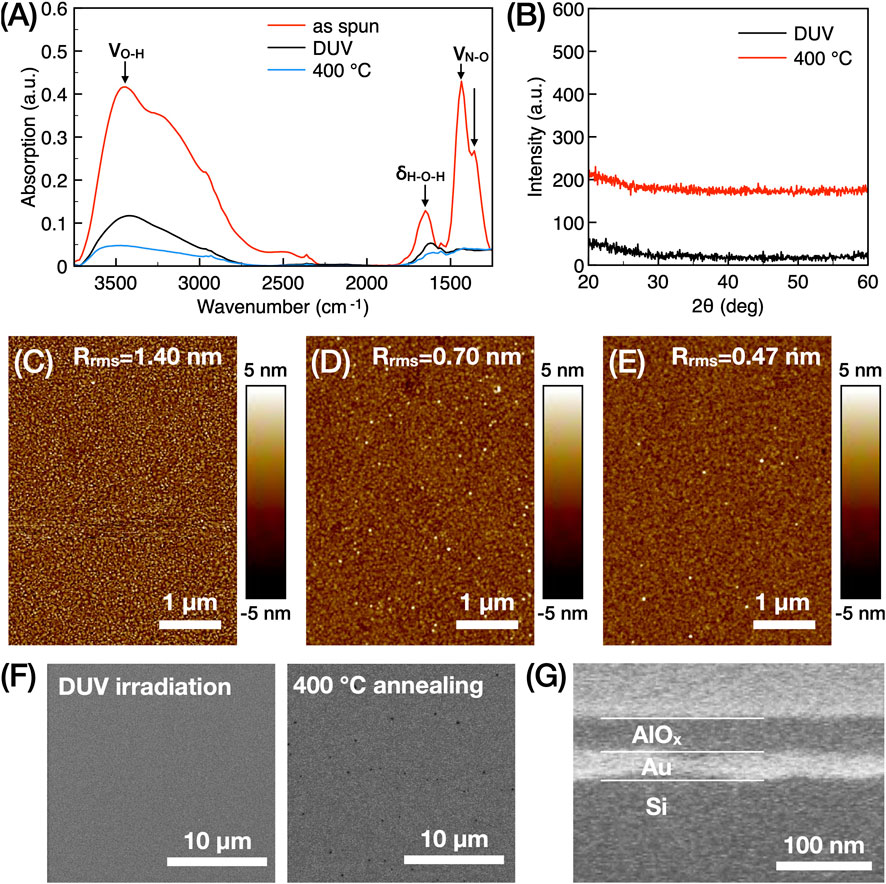
FIGURE 2. (A) FTIR of the as-spun sample, DUV-treated, and high-temperature annealing samples. (B) In-plane XRD of DUV-treated and high-temperature annealing samples. (C–E) AFM images of the surface morphology of Au thin film evaporated on glass, AlOx surface morphology of DUV-treated and high-temperature annealing samples, respectively. (F) Surface morphology of AlOx thin film prepared by DUV irradiation and high temperature annealing, respectively. (G) Cross-section SEM image of AlOx thin film.
After obtaining pinhole-free and densely packed AlOx thin film, we characterized the electrical strength and the capacitance of the dielectric layer. A MIM structure (Au/AlOx/Au) is used for leakage current and capacitance measurements. As shown in Figure 3A, an extremely low leakage current density across the AlOx thin film of 10−9 A/cm2 is obtained for a 1 MV/cm electric field for both DUV-treated and high-temperature annealed samples, indicating the good insulating property of AlOx thin film. The leakage current density for the high-temperature annealed sample remains almost unchanged up to 3.5 MV/cm, but slightly increases for the DUV-treated sample. This suggests that high-temperature annealing plays a critical role in maintaining good insulation in a higher electric field; the sample prepared by DUV probably has remaining hydroxyl groups in the thin film, as shown in the FTIR images in Figure 2A, thus showing a worse leakage property. Nevertheless, without using a phosphonic acid-based self-assembly monolayer that could greatly enhance the electrical strength (Klauk et al., 2007; Kraft et al., 2015), the maximum leakage current density of the DUV-treated samples achieved in this work is 8 × 10⁻⁹ A/cm2 at 3.5 MV/cm, which is among the best reported value in recent work (Kaltenbrunner et al., 2013; Park et al., 2015; Jinno et al., 2017). It is worth noting that the voltage sweeping speed for I–V measurement is sufficiently slow enough that the displacement current generated by dV/dt can be suppressed in a way that does not affect the accuracy of the current reading. The good electrical strength of DUV-treated AlOx thin film proves the effective low-temperature solidification of metal-oxide by DUV light. Next, we performed a capacitance-frequency measurement for the DUV-treated dielectric layer. The same MIM device was measured and the result is plotted in Figure 3B. Within the measurement range of 1 kHz–1 MHz, the average unit-area capacitance is around 180 nF/cm2 for 40 nm-thick AlOx, which is 16 times higher than the commonly used 300 nm SiO2 dielectric (11.5 nF/cm2). Thus, the relative permittivity at 1 kHz is calculated based on the following equation:
where Ci is the unit-area capacitance of AlOx thin films, d is the thickness of AlOx, and
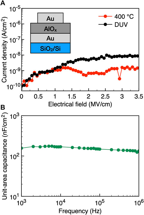
FIGURE 3. (A) Leakage current density of AlOx dielectric thin film by high temperature annealing and DUV irradiation, the inset is a schematic drawing of the MIM device structure. (B) Unit-area capacitance of AlOx dielectric thin film by DUV irradiation.
The transistor device is completed by the thermal evaporation of C10-DNTT organic small molecules and the Au top contact; Figure 4A is a schematic drawing of the device structure. Benefiting from the large unit-area capacitance of the AlOx dielectric, the transistor can reach saturation state at −3 V gate bias. As the transfer I–V curve shows in Figure 4B, the channel current is >2 μA at its saturation state and the on/off current ratio is 4 × 10⁵. The low off-state current at around 5 pA indicates good insulation of the dielectric layer, which is also important for lowering the device’s static power consumption (Ren et al., 2018). The transistor exhibits a sharp turn-on with a steep sub-threshold swing of 110 mV/dec and very small hysteresis. Both results suggest low trap states’ density at the organic semiconductor/dielectric interface, which could be attributed to the atomic smooth surface of the AlOx dielectric formed by the sol-gel method. The field-effect mobility (μ) in the saturation region is obtained by the following equation:
where Ci is the unit-area capacitance (at 1 kHz) of the dielectric layer and Vth is the threshold voltage. The threshold voltage is determined to be −0.72 V by the x-axis intercept of the tangent of IDS1/2 against the VGS curve (Figure 4B). Thus, a carrier mobility of 1.8 cm2/Vs is achieved at a −3 V gate bias. This value is comparable to those OFETs based on the same organic material on SAM modified AlOx dielectric (Kraft et al., 2015). The hysteresis shown in the transfer I-V is probably due to the residual solvent in dielectric film that act as charge trapping centers. In addition, the output I–V curve shown in Figure 4C has slight nonlinearity in the small VDS region, which indicates that the Schottky injection barrier may exist in the drain–source contact. The device’s performance could be further improved by optimizing the charge injection. The bias stress characterization of OFET is plotted in Figure 4D. After applying 3,000 s gate bias at −3 V, only a slight negative shift of threshold voltage is observed, suggesting good bias stress stability of the device. The good electrical performance with high mobility and steep sub-threshold swing of the C10-DNTT/AlOx OFET demonstrates excellent interfacial properties and that high-quality sol-gel oxide thin film can be obtained via DUV photoactivation.
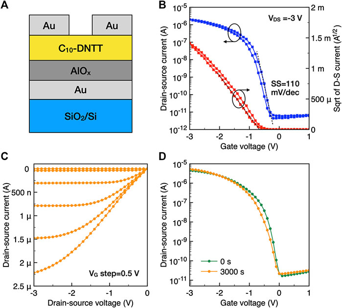
FIGURE 4. (A) Schematic drawing of the organic transistor device structure. (B) Transfer I-V curve and square root of the drain-source current of the organic transistor. (C) Output I-V curve of the organic transistor. (D) Bias stress stability of the organic transistor.
The relatively low processing temperature allows the device to be fabricated on various flexible substrates. To demonstrate the flexible device application, we applied the same device structure and fabrication steps on a 125 μm-thick flexible PEN substrate. Transistors on a PEN substrate can saturate at −2 V gate bias while showing a decreased carrier mobility of 0.6 cm2/Vs. This is probably due to the larger surface roughness of a bare PEN substrate (Rrms = 3.60 nm, Figure 5B) that scatters the charge transport at the channel region. Figures 5A,C show the optical image of the transistor at the bending state and the transfer I–V curves at the bending and flat state, respectively. Compared to the thickness of the PEN substrate, the thickness of AlOx and the organic layer is three orders of magnitude smaller; therefore, the tensile strain (ε) applied on the channel and dielectric at an upward bending radius of 9 mm (Figure 5A) can be estimated as 0.69% based on the equation ε = d/2R where d is the total substrate thickness and R is the bending radius. The transfer I–V curves are almost identical in the bending and flat states (Figure 5C). The results prove no cracks or other defects form during bending, so the device’s performance remains unchanged. The solution-processed high-k dielectric is fully compatible with a flexible substrate.
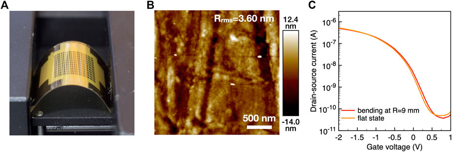
FIGURE 5. (A) optical image of the flexible organic transistor device under upward bending; the bending radius is 9 mm. (B) AFM image of the surface morphology of PEN substrate. (C) Transfer I-V curve of the flexible organic transistor at bending and flat states.
Conclusions
In summary, we have developed a facile low-temperature solution preparation of a AlOx dielectric thin film. The as-fabricated AlOx dielectric has a high permittivity of 8.3 (at 1 kHz) and a low leakage current of 8 × 10⁻⁹ A/cm2 at 3.5 MV/cm, which is sufficiently robust for transistor applications. The operating voltage of the OFET is below −3 V, with a saturation mobility of 1.8 cm2/Vs, steep sub-threshold swing of 110 mV/dec, and negligible hysteresis. The device can also be fabricated using a flexible PEN substrate and shows almost identical electrical characteristics in the flat state and at a 9 mm bending radius. Our results suggest that the simple low-temperature DUV process can offer high-performance AlOx dielectric thin film that can be used for transistor devices to significantly reduce the device’s dynamic power consumption. This process can be easily scaled-up for continuous, industrial-level production and thus provides a promising approach for low-cost and high-performance organic electronic devices.
Data Availability Statement
The raw data supporting the conclusions of this article will be made available by the authors, without undue reservation.
Author Contributions
WH, XR, and XZ conceived and designed the experiments. QM fabricated the dielectric sample, performed FTIR and XRD measurements, and carried out data analysis. QM and ZC performed AFM measurement and transistor device fabrication. SD performed the flexible device measurement. WH directed the project. All authors discussed the results and co-wrote the manuscript.
Funding
The authors acknowledge financial support from the National Key R&D Programs (2017YFA0204503, 2016YFB0401100) and the National Natural Science Foundation of China (91833306, 51633006, 51703159, 51703160, 51733004).
Conflict of Interest
The authors declare that the research was conducted in the absence of any commercial or financial relationships that could be construed as a potential conflict of interest.
Acknowledgments
We thank Prof. Yu Xi for useful advice on DUV light source selection.
References
Bolot, S., Fuchs, P., Knobelspies, S., Temel, O., Sevilla, G. T., Gilshtein, E., et al. (2019). Inkjet-Printed and deep-UV-annealed YAlOx dielectrics for high-performance IGZO thin-film transistors on flexible substrates. Adv. Electron. Mater. 5, 1800843. doi:10.1002/aelm.201800843
Diao, Y., Tee, B. C. K., Giri, G., Xu, J., Kim, D. H., Becerril, H. A., et al. (2013). Solution coating of large-area organic semiconductor thin films with aligned single-crystalline domains. Nat. Mater. 12, 665–671. doi:10.1038/nmat3650
Duan, S., Wang, T., Geng, B., Gao, X., Li, C., Zhang, J., et al. (2020). Solution-processed centimeter-scale highly aligned organic crystalline arrays for high-performance organic field-effect transistors. Adv. Mater. 32, 1908388. doi:10.1002/adma.201908388
Heo, J., Park, S. Y., Kim, J. W., Song, S., Yoon, Y. J., Jeong, J., et al. (2018). Implementation of low-power electronic devices using solution-processed tantalum pentoxide dielectric. Adv. Funct. Mater. 28, 1704215. doi:10.1002/adfm.201704215
Hussain, F., Park, S., Jeong, J., Kang, S. J., and Kim, J. (2020). Structure–property relationship of poly(cyclohexane 1,4‐dimethylene terephthalate) modified with high trans‐1,4‐cyclohexanedimethanol and 2,6‐naphthalene dicarboxylicacid. J. Appl. Polym. Sci. 137, 48950. doi:10.1002/app.48950
Jiang, C., Choi, H. W., Cheng, X., Ma, H., Hasko, D., and Nathan, A. (2019). Printed subthreshold organic transistors operating at high gain and ultralow power. Science 363, 719–723. doi:10.1126/science.aav7057
Jinno, H., Yokota, T., Matsuhisa, N., Kaltenbrunner, M., Tachibana, Y., and Someya, T. (2017). Low operating voltage organic transistors and circuits with anodic titanium oxide and phosphonic acid self-assembled monolayer dielectrics. Org. Electron. 40, 58–64. doi:10.1016/j.orgel.2016.10.034
Jo, J. W., Kim, K. H., Kim, J., Ban, S. G., Kim, Y. H., and Park, S. K. (2018). High-mobility and hysteresis-free flexible oxide thin-film transistors and circuits by using bilayer sol-gel gate dielectrics. ACS Appl. Mater. Interfaces. 10, 2679–2687. doi:10.1021/acsami.7b10786
Kaltenbrunner, M., Sekitani, T., Reeder, J., Yokota, T., Kuribara, K., Tokuhara, T., et al. (2013). An ultra-lightweight design for imperceptible plastic electronics. Nature 499, 458–463. doi:10.1038/nature12314
Klauk, H., Zschieschang, U., Pflaum, J., and Halik, M. (2007). Ultralow-power organic complementary circuits. Nature 445, 745–748. doi:10.1038/nature05533
Kraft, U., Sejfic, M., Kang, M. J., Takimiya, K., Zaki, T., Letzkus, F., et al. (2015). Flexible low-voltage organic complementary circuits: finding the optimum combination of semiconductors and monolayer gate dielectrics. Adv. Mater.27, 207–214. doi:10.1002/adma.201403481
McKerricher, G., Maller, R., Mohammad, V., McLachlan, M. A., and Shamim, A. (2017). Inkjet-printed thin film radio-frequency capacitors based on sol-gel derived alumina dielectric ink. Ceram. Int. 43, 9846–9853. doi:10.1016/j.ceramint.2017.04.167
Mullapudi, G. S. R., Velazquez-Nevarez, G. A., Avila-Avendano, C., Torres-Ochoa, J. A., Quevedo-López, M. A., and Ramírez-Bon, R. (2019). Low-temperature deposition of inorganic-organic HfO2-PMMA hybrid gate dielectric layers for high mobility ZnO thin-film transistors. ACS Appl. Electron. Mater. 1, 1003–1011. doi:10.1021/acsaelm.9b00175
Park, J. W., Kang, B. H., and Kim, H. J. (2020). A review of low-temperature solution-processed metal oxide thin-film transistors for flexible electronics. Adv. Funct. Mater. 30:1904632. doi:10.1002/adfm.201904632
Park, S., Kim, C.-H., Lee, W.-J., Sung, S., and Yoon, M.-H. (2017). Sol-gel metal oxide dielectrics for all-solution-processed electronics. Mater. Sci. Eng. R Rep. 114, 1–22. doi:10.1016/j.mser.2017.01.003
Park, S., Kim, K. H., Jo, J. W., Sung, S., Kim, K. T., Lee, W. J., et al. (2015). In-depth studies on rapid photochemical activation of various sol-gel metal oxide films for flexible transparent electronics. Adv. Funct. Mater. 25, 2807–2815. doi:10.1002/adfm.201500545
Quah, H. J., Cheong, K. Y., Hassan, Z., and Lockman, Z. (2010). MOS characteristics of metallorganic-decomposed CeO2 spin-coated on GaN. Electrochem. Solid-State Lett. 13, H116–H118. doi:10.1149/1.3290679
Quah, H. J., Hassan, Z., Yam, F. K., Ahmed, N. M., Salleh, M. A. M., Matori, K. A., et al. (2017). Effects of ammonia-ambient annealing on physical and electrical characteristics of rare earth CeO2 as passivation film on silicon. J. Alloys Compd. 695, 3104–3115. doi:10.1016/j.jallcom.2016.11.339
Ren, X., Yang, F., Gao, X., Cheng, S., Zhang, X., Dong, H., et al. (2018). Organic field-effect transistor for energy-related applications: low-power-consumption devices, near-infrared phototransistors, and organic thermoelectric devices. Adv. Energy Mater. 8, 1801003. doi:10.1002/aenm.201801003
Sun, Q.-J., Li, T., Wu, W., Venkatesh, S., Zhao, X.-H., Xu, Z.-X., et al. (2019). Printed high-k dielectric for flexible low-power extended gate field-effect transistor in sensing pressure. ACS Appl. Electron. Mater. 1, 711–717. doi:10.1021/acsaelm.9b00081
Sung, S., Park, S., Lee, W. J., Son, J., Kim, C. H., Kim, Y., et al. (2015). LowVoltage flexible organic electronics based on high-performance sol gel titanium dioxide dielectric. ACS Appl. Mater. Interfaces. 7, 7456–7461. doi:10.1021/acsami.5b00281
Wang, S. M., Yao, S. S., Lin, J. S., and Xia, G. D. (2019). Eco-friendly, low-temperature solution production of oxide thin films for high-performance transistors via infrared irradiation of chloride precursors. Ceram. Int. 45, 9829–9834. doi:10.1016/j.ceramint.2019.02.021
Wang, Z., Ren, X., Leung, C. W., Shi, S., and Chan, P. K. L. (2013). A UV-ozone treated amorphous barium-strontium titanate dielectric thin film for low driving voltage flexible organic transistors. J. Mater. Chem. C. 1, 3825–3832. doi:10.1039/c3tc30345d
Wang, Z. R., Ren, X. C., Fan, C. C., Chang, Y. H., Li, H. Y., Chen, H. Z., et al. (2014). Low cost universal high-k dielectric for solution processing and thermal evaporation organic transistors. Adv. Mater. Interfaces. 1, 1300119. doi:10.1002/admi.201300119
Xia, G. D., and Wang, S. M. (2019). Rapid and facile low-temperature solution production of ZrO2 films as high-k dielectrics for flexible low-voltage thin-film transistors. Ceram. Int. 45, 16482–16488. doi:10.1016/j.ceramint.2019.05.181
Xia, W. W., Xia, G. D., Tu, G. S., Dong, X., Wang, S. M., and Liu, R. (2018). Sol-gel processed high-k aluminum oxide dielectric films for fully solution-processed low-voltage thin-film transistors. Ceram. Int. 44, 9125–9131. doi:10.1016/j.ceramint.2018.02.120
Yamamura, A., Watanabe, S., Uno, M., Mitani, M., Mitsui, C., Tsurumi, J., et al. (2018). Wafer-scale, layer-controlled organic single crystals for high-speed circuit operation. Sci. Adv. 4, eaao5758. doi:10.1126/sciadv.aao5758
Keywords: power consumption1, sol-gel2, high-k dielectric3, AlOx4, organic field‐effect transistor
Citation: Mu Q, Chen Z, Duan S, Zhang X, Ren X and Hu W (2020) A Low-Temperature Solution-Process High-k Dielectric for High-Performance Flexible Organic Field-Effect Transistors. Front. Mater. 7:570002. doi: 10.3389/fmats.2020.570002
Received: 05 June 2020; Accepted: 11 September 2020;
Published: 16 November 2020.
Edited by:
Jia Huang, Tongji University, ChinaReviewed by:
Xiaojun Guo, Shanghai Jiao Tong University, ChinaHock Jin Quah, University of Science Malaysia, China
Copyright © Mu, Chen, Duan, Zhang, Ren and Hu. This is an open-access article distributed under the terms of the Creative Commons Attribution License (CC BY). The use, distribution or reproduction in other forums is permitted, provided the original author(s) and the copyright owner(s) are credited and that the original publication in this journal is cited, in accordance with accepted academic practice. No use, distribution or reproduction is permitted which does not comply with these terms.
*Correspondence: Xiaochen Ren, renxiaochen@tju.edu.cn; Wenping Hu, huwp@tju.edu.cn