
Abstract
FAPbI3(NH2CHNH2PbI3) is an organic-inorganic hybrid perovskite containing Pb, which has good photoelectric characteristics and great potential in the application of low-cost and high energy efficiency photoelectric devices. In order to reduce the pollution of Pb to the environment, the first-principles based on density functional theory(DFT) is used to compare and study the photoelectric parameters such as the band structure, density of states(DOS), absorption coefficient, reflectivity, conductivity and dielectric function of FAPb1−xGexI3(x = 0.0,0.33,0.50,0.67,1.0). The results show that the 4p orbital electrons of Ge and the 6p orbital electrons of Pb and 5p orbital electrons of I are hybridized after doped with Ge, which change the band structure of FAPbI3. The result is that the optical band gap of the material is narrowed, the curvature of the band is increased, the effective mass of electrons and holes is reduced, the absorption peak of visible light increases and the absorption range increases. And the reflectivity and energy loss of the material also increase at the same time. The super SOC effect of the heavy metal Pb element leads to the splitting of the conduction band level of FAPbI3, the conduction band value drops sharply, and the band gap decreases sharply. We found that when the doping ratio of x in FAPb1−xGexI3 was between 0.55 and 0.65, the optimal band gap was between 1.3–1.4 eV. Therefore, reasonable regulation of Ge's doping ratio can improve the photoelectric conversion efficiency of FAPbI3. This study can provide some theoretical guidance for experimental research and search for new efficient and environmentally friendly perovskite solar materials.
Export citation and abstract BibTeX RIS

Original content from this work may be used under the terms of the Creative Commons Attribution 4.0 licence. Any further distribution of this work must maintain attribution to the author(s) and the title of the work, journal citation and DOI.
1. Introduction
With the continuous growth of the world's population, the demand for energy is increasing, and the problem of energy shortage is becoming more and more serious. It is urgent to find a new renewable and pollution-free energy, and solar energy has become one of its first choices [1–9]. In 2009, Kojima et al first prepared perovskite-type organic-inorganic hybrid materials to replace organic molecules as light-absorbing materials for solar cells (efficiency 3.8%) [1]. On August 3, 2019, Newport, authorized by the US national renewable energy laboratory, released a certified maximum efficiency of 25.2% for a single perovskite solar cell [10]. Organic-inorganic hybrid perovskite provides the possibility for the preparation of low-cost and high-efficiency solar energy devices [11]. Perovskite materials with ABX3 structure have attracted many researchers due to their high efficiency in absorbing light [8, 12]. Where A is an organic or inorganic cation such as MA=CH3NH3, FA=NH2CHNH2, Cs, B is a metal ion such as Pb, Sn, Ge, and X is a halide anion or halide mixture such as I, Br, Cl, I-Br. The ABX3 structure of organic-inorganic hybrid perovskite solar cells generally consists of metal atoms as octahedral core, halogen atoms as octahedral top angles, and organic molecules at the top angles of the face-centered cubic lattice. The halogen octahedron is composed of three-dimensional shapes with common vertex connections. According to the connection rules of coordination polyhedron, this structure is more stable than the structure with common edges and co-planar. In addition, the co-vertex connection structure makes the gap between the octahedral meshes larger than the gap between the co-edge and co-planar structures, which can allow larger ions to fill in.
In the past 10 years, perovskite FAPbI3 has been widely used as the absorption layer of solar energy, mainly due to its advantages of wide absorption range, suitable band gap, superior photoelectric property, low cost and high photoelectric conversion efficiency [13–15]. FAPbI3 has three crystal structures, which are orthogonal structure, tetragonal structure and face-centered cubic structure. It is an orthogonal structure at low temperature of 161k, transforms into a tetragonal structure at normal temperature of 300k and a face-centered cubic structure at 327–330k [16–18]. Farhad Fouladi Targhi et al studied hybrid organic-inorganic perovskite photovoltaic materials MAPbI3 and FAPbI3 and found that the electronic band gap of FAPbI3 (1.43 eV) was more qualified than MAPbI3 (1.64 eV) and suitable to be applied in high performance photovoltaic devices [19]. Mahnaz Mozaffari et al used sequential deposition method to prepare FAPbI3 and MAPbI3 perovskite films as light absorbers in solar cells. It was found that controlling the temperature of the FAI solution at 80 °C would lead to the formation of a stable black FAPbI3 perovskite layer, affecting the photovoltaic parameters of FAPbI3 perovskite solar cells [20]. Wang et al used the first-principles to study the structural, electronic, and elastic properties of cubic FAPbI3 perovskite. It showed that FAPbI3 was mechanically stable and ductile and had weaker strength of the average chemical bond [21].
At present, FAPbI3 has the narrowest optical band gap of 1.48 eV among the widely studied organic-inorganic hybrid perovskite materials, which is still greater than the theoretical value of 1.34 eV of the ideal single-junction solar cell [22, 23]. In order to further improve the photoelectric conversion efficiency of perovskite solar cells, the preparation of light-absorbing materials with band gap close to the ideal value has become a research hotspot. The formation of perovskite alloy materials with adjustable band gap by replacing A, B and X ions with ions of similar size has attracted more and more attention in academic circles. Since Pb, Ge and Sn are elements in the same main group, they have similar electron shells, and they have the same number of electrons in their outermost shell (both two electrons), so they are similar in many properties. Both theory and experiment show that it is feasible to replace Pb with Ge and Sn. Pushar Kanhere et al used the first-principles to calculate MAPbI3 doped with Sn, and found that Sn's doping would change the band structure, the effective mass of electrons and holes of perovskite [24]. This provides a theoretical basis for improving the photoelectric conversion efficiency of perovskite. Diao et al studied the photoelectric property of FA1−xCsxPbI3 through the first-principles, and found that there was the most suitable band gap of 1.45 eV when x = 0.25, but it was still slightly higher than the optimal band gap value [25]. There are many reports such as MAxFA1−xPbI3, CsxMA1−xPbI3, FAPb(I1−xBrx)3 and other materials whose band gap is larger than the ideal theoretical value. Up to now, there are only a few perovskite materials with close to 1.34 eV in the literature, such as MAPb(I1−xBrx)3, (MAPbI3)x(FAPbI3)1−x, (FAPbI3)x(MAPbBr3)1−x etc, but these materials have potential stability problems due to the volatilization of methyl ammonia ions (MA+) and other factors [26–28]. So they are difficult to be applied commercially. In order to find the best band gap of photoelectric material, we further studied the doping of FAPbI3 based on the first-principles of DFT. Firstly, we calculated and analyzed the band structure, DOS, surface charge density and absorption coefficient of FAPbI3. Then we focused on the calculation of the photoelectric parameters such as the band structure, DOS, absorption coefficient, reflectivity, conductivity and dielectric function of FAPb1−xGexI3(x = 0.0, 0.33, 0.50, 0.67, 1.0) of the tetragonal structure. It is found that FAPbI3 doped with Ge can greatly improve its photoelectric performance. As long as the doping ratio of Ge is well regulated, the band gap width can reach the ideal value of 1.34 eV, the higher photoelectric conversion efficiency will be obtained [23]. This can provide a certain reference for searching for new high-efficient perovskite solar absorption layer materials.
2. Calculation method
Based on the first-principles plane wave pseudo-potential method [29, 30] in DFT, the Cambridge Sequential Total Energy Package (CASTAP) module was used to calculate. The electronic exchange-correlations were treated by the Perdew–Burke–Ernzerhof (PBE) under generalized gradient approximation (GGA) [31], and the OTFG Ultrasoft pseudo-potential was used to describe the interaction between electrons and ions [32]. For solids, especially doped solids, the fully relaxed structures with highly converged total energies, forces and stresses play crucial roles in the studies of their electronic structures as well as optical properties. Accordingly, geometry optimization is essential to obtain their stable states of the relaxed structures, meaning that strict convergence criteria must be satisfied in the relaxation of atomic positions and lattice parameters [33]. The integration calculation of the system in Brillouin region uses the monkhorst-pack scheme, the k grid point is 2 × 2 × 2 [34] and the cut-off energy of plane wave of the system is set at 435 eV to ensure the convergence of energy and configuration of the system at the level of quasi-complete plane wave base. In the self-consistent field operation, Pulay density mixing method is adopted, and the self-consistent field is set as 5 × 10⁻⁷ eV/atom. Broyden-Fletcher-Goldfarb-Shanno(BFGS) algorithm was used for the structural optimization of the model with following optimization parameters: the convergence standard of interatomic interaction as 0.05 eV Å−1, the convergence standard of monatomic energy as 2 × 10⁻⁵ eV, the convergence criterion of internal stress in crystal as 0.1 GPa and the convergence criterion of maximum atomic displacement as 0.002 Å. The program optimizes the four parameters simultaneously and achieves the convergence standard. The valence electrons involved in the calculation are H-1s1, C-2s22p2, N-2s22p3, Ge-4s24p2, Pb-6s26p2 and I-5s25p5, respectively.
3. Results and discussion
3.1. Pure FAPbI3
Park et al [35] prepared FAPbI3 as the light-absorbing layer material of solar cells by replacing MA with FA, and found that the decomposition temperature of perovskite material FAPbI3 was more than 50 °C higher than that of perovskite material MAPbI3. FAPbI3 has better thermal stability and higher photoelectric conversion efficiency than MAPbI3. FAPbI3 has three typical crystal structures shown in figure 1, whose formation is determined by temperature.

Figure 1. Three typical crystal structures of (a) cubic (b) tetragonal and (c) orthogonal of FAPbI3.
Download figure:
Standard image High-resolution imageFAPbI3, as an absorption layer of solar cells, plays a key role in the photoelectric conversion efficiency of solar cells. The four basic parameters of solar cells are the short circuit current JSC , the open circuit voltage Voc, the filling factor FF and the photoelectric conversion efficiency η, respectively.

Where  is the power of incident light. Microscopically, the incident monochromatic photon-electron conversion efficiency (IPCE) satisfies the formula:

Here LHE is the light capture efficiency,  is the quantum yield of electron injection and
  is the charge collection rate on the contact surface of the conductive substrate.
3.1.1. Band structure and DOS
The photoelectric conversion efficiency of solar cells is related to the band structure and photoelectric property of materials. Figures 2 and 3 show the band structure and DOS of FAPbI3. It can be seen that there is no obvious difference between the conduction band of the three structures. The conduction band near the Fermi surface is mainly contributed by the electrons of Pb 6p orbital, while the deep conduction band is mainly contributed by the electrons of I 5s and Pb 6s orbitals. The valence band of the three structures is different, mainly contributed by the electrons of I 5p orbital. The valence band DOS near the Fermi surface of the tetragonal structure is significantly higher than that of the other two structures, and the electrons DOS of the 5p orbital of I is also significantly higher. This indicates that the valence band of I near the Fermi surface of the tetragonal structure is more localized than that of the other two structures. The energy states of other elements in FA are mainly distributed in the deep energy level below −5 eV and the DOS distribution is sharp, strong local and not involved in bonding, so their contribution to the DOS near the Fermi surface is almost zero. It shows that the covalent interaction between the organic ions FA+ and Pb2+, I− is weak and not as strong as that between Pb2+ and I−, but FA+ is crucial to the stability of crystal structure. The stability tolerance factor of ABX3 is given by the Goldschmidt equation  [36]. The closer T is to 1, the more stable the crystal structure. Since the radius of Pb2+ at position B is relatively large, it is difficult to find a single element A with A matching radius. The radius size of organic molecule group FA+ is similar to that of Pb2+, and the tolerance factor T of FAPbI3 is 0.99, so it is quite stable.

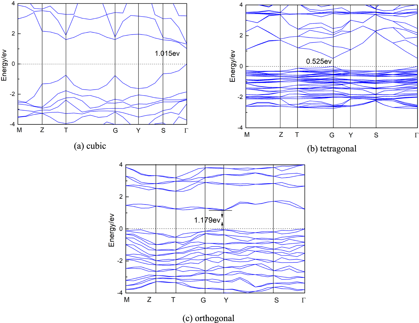
Figure 2. Band structure of three structures of (a) cubic (b) tetragonal and (c) orthogonal of FAPbI3.
Download figure:
Standard image High-resolution image
Figure 3. DOS of three structures of (a) cubic (b) tetragonal and (c) orthogonal of FAPbI3.
Download figure:
Standard image High-resolution imageIt is found that the super strong spin–orbit coupling (SOC) effect will reduce the conduction band when calculating the band structure of materials containing heavy elements. Because FAPbI3 contains the heavy element Pb, the super strong spin–orbit coupling effect cannot be ignored in the calculation of band structure [37, 38]. As can be seen from figure 4, the energy level drops significantly when the SOC effect is taken into account. The band structure values of three FAPbI3 structures with and without SOC effect are given in table 1. It can be seen from table 1 that the band gap width of FAPbI3 of cubic structure is 1.537 eV without considering SOC effect, slightly higher than the experimental value of 1.48 eV, but within the acceptable range. This indicates that it is feasible for us to use PBE in GGA as exchange association functional, and it is not necessary to use HSE06 with higher precision. It can be seen from the band structure diagram that the conduction band is mainly affected by the SOC effect, which destroys the degeneracy of the conduction band and causes the energy level to split and move down significantly, while the valence band is basically unaffected. At the same time, it was found that the symmetry of the geometric structure of the system would be enhanced as the number of delocalized electrons increased after considering the SOC effect. Based on this, we found that the band gap width of three structures were only 1.015 eV, 0.525 eV and 1.179 eV after considering SOC effect. It is worth noting that the band structure of the tetragonal structure is more affected by the SOC effect, and its band gap value is only 0.525 eV. It is obvious that the relativistic effect of the system can not be ignored after the SOC effect is taken into account, so the electronic structure of the system has changed. However, it is far from the experimental value after considering the SOC effect, so we do not consider the SOC effect in the following studies.

Figure 4. The band structure of three structures of (a) cubic (b) tetragonal and (c) orthogonal of FAPbI3 with SOC.
Download figure:
Standard image High-resolution imageTable 1. Band gap of FAPbI3 without SOC compared with SOC.
| FAPbI3 | Cubic | Tetragonal | Orthogonal |
|---|---|---|---|
| Band gap(without SOC) | 1.537 eV | 1.626 eV | 1.747 eV |
| Band gap(with SOC) | 1.015 eV | 0.525 eV | 1.179 eV |
3.1.2. Surface charge density
Figure 5 shows the distribution of charge density of three crystal structures of FAPbI3. Blue represents the outside of the isosurface, gray represents the inside of the isosurface, and yellow points represent the electron clouds (the possible positions of electrons). From the color and shape of the isosurface and the distribution of the electron clouds, we can see that the charge is mainly concentrated on FA+, Pb2+ and I−, in which the electron clouds of Pb2+ and I− overlap obviously, while FA+ is almost isolated. This indicates that Pb2+ and I− have stronger effects, which is consistent with the previous analysis results.

Figure 5. The distribution of charge density of three crystal structures of (a) cubic (b) tetragonal and (c) orthogonal of FAPbI3.
Download figure:
Standard image High-resolution image3.1.3. Absorption coefficient
As can be seen from figure 6, the absorption coefficients of the three structures are not significantly different. The absorption effect of orthogonal structure is the best in the ultraviolet region, while the absorption effect of tetragonal structure is the best in the visible and infrared region. By comparing the solar spectrum, it can be seen that the tetragonal structure is the best for solar energy absorption among the three crystal structures.

Figure 6. Absorption spectra of three structures of FAPbI3.
Download figure:
Standard image High-resolution image3.2. FAPbI3 doping with Ge
As the heavy metal Pb in FAPbI3 is harmful to both human and environment, it is particularly important to explore a kind of high-efficient perovskite material with no lead or little lead. The most ideal elements to replace Pb are Ge and Sn in the same main group. Since Sn2+ is unstable in the electron pairing in perovskite, it is easy to be oxidized to Sn4+, which leads to the battery failure. Therefore, this paper studies the doping of Ge in FAPbI3. Due to the higher absorption coefficient of FAPbI3 in the range of visible light at room temperature and the limited space, we only choose FAPbI3 crystal in the tetragonal structure for doping study. In the future work, we will continue to study the doping of the other two structures. Figure 7 is the super-cell structure doped with Ge. We doped Ge according to the ratio of 0, 0.33, 0.5, 0.67 and 1 of the total number of Pb atoms in FAPbI3.

Figure 7. The super-cell of FAPbI3 of 2 × 1 × 1 after doping with Ge.
Download figure:
Standard image High-resolution image3.2.1. Crystal structures
From the calculated data in table 2, it can be seen that with the doping of Ge, the crystal structure changes significantly. The change rules are summarized as follows:
- 1.The change in the lattice constant results in a significant change in the volume of the crystal. With the increase of Ge's doping ratio, the crystal volume first increased and then decreased, and the volume of pure FAGeI3 was smaller than that of pure FAPbI3. We know that the radius of Ge2+ (0.073 nm) is smaller than the radius of Pb2+ (0.119 nm), but both Ge2+ and Pb2+ have repulsion effects at the same time. When repulsion is dominant, the volume increases and vice versa. From the calculated data in table 2, it can be seen that the repulsion of Ge2+ and Pb2+ plays a major role as the doping ratio is before 0.5, so the volume increased first and then decreased. It is worth noting that the volume of pure FAGeI3 is smaller than that of pure FAPbI3, because we don't care about repulsion, we just care about the radius of the ions.
- 2.The space group changed after Ge's doping, but the pure FAPbI3 and the pure FAGeI3 space group were the same, and both were P42/MNM.
- 3.The cell angle doesn't change, and it's all 90°.
- 4.
Table 2. Calculated the lattice constant, volume, space group, cell angle and tolerance factor(T) of FAPb1−xGexI3(x = 0.0,0.33,0.5,0.67,1.0).
| a(Å) | b(Å) | c(Å) | V(Å3) | Space group | α = β = γ (°) | T | |
|---|---|---|---|---|---|---|---|
| FAPbI3 | 9.38 | 9.38 | 12.85 | 1130.95 | P42/MNM | 90 | 0.99 |
| FAPb0.67Ge0.33I3 | 9.48 | 12.70 | 18.83 | 2267.85 | P 1 M 1 | 90 | 1.04 |
| FAPb0.5Ge0.5I3 | 12.48 | 19.17 | 9.80 | 2343.84 | P M N 21 | 90 | 1.06 |
| FAPb0.33Ge0.67I3 | 9.20 | 9.20 | 12.48 | 1056.48 | P4/MMM | 90 | 1.09 |
| FAGeI3 | 8.89 | 8.89 | 12.08 | 953.65 | P42/MNM | 90 | 1.10 |
3.2.2. Band structure and DOS
Figure 8 shows the band structure of FAPb1−xGexI3 after different doping ratio (x = 0.33, 0.5, 0.67, 1). It can be seen that FAPb1−xGexI3 is a direct band gap semiconductor and the conduction band and valence band of FAPb1−xGexI3 have changed after doped with Ge.
- 1.The change of conduction band is more obvious than that of valence band after doping. With the increase of Ge's doping ratio, the conduction band near the Fermi surface become denser first and then sparser. After all Pb are replaced by Ge, the conduction band near the Fermi surface is the same as before without doping. Combined with the partial density of states(pDOS) distribution in figure 9, it can be seen that the 4p orbital electrons of Ge and the 6p orbital electrons of Pb in the conduction band become hybridized after doping with Ge, which leads to the increased contribution of electrons to the conduction band, and the density of electrons becomes dense. With the increase of the Ge's doping ratio, the content of Pb decreases correspondingly, and the hybridization will gradually weaken, which leads to the gradual decrease of electron contribution. When Ge completely replaces Pb, Ge's contribution to the conduction electrons near Fermi surface is similar to that of Pb, so that the conduction band near Fermi surface in the band structure diagram becomes as sparse as before.
- 2.As the increase of doping ratio, the band gap increases first and then decreases gradually. There are two reasons as follows. (1) When x is less than 0.5, Ge's 4p orbital electrons and Pb's 6p orbital electrons are hybridized in the deep energy level of the conduction band, and their contribution to the DOS of the conduction band near Fermi surface is less than that of pure Pb's 6p orbital electrons. (2) When x is less than 0.5, I'5p orbital electrons contribute more to the valence band near the Fermi surface, while when x > 0.5, the corresponding contribution gradually decreases, as shown in table 3. For the valence band near the Fermi surface, the greater the contribution of I, the stronger the nonmetal property, which leads to the decrease of the valence band and the increase of the band gap width. With the increase of the proportion of Ge, the contribution of its 4p orbital electrons to the DOS near the Fermi surface gradually increases, and the hybridization of Ge's 4p orbital electrons with Pb's 6p orbital electrons also becomes stronger and stronger, so that the material shows more and more obvious metallic properties and the conduction band decreases significantly. However, at the same time, the contribution of I's 5p orbital elections to the valence band near Fermi surface also decreases and the valence band does not decrease, so the band gap gradually decreases.
- 3.Doping Ge will affect the smoothness of conduction and valence band. The smoothness is the curvature of the curve. According to the formula:


Where 
 and
and  are the coefficient,
  is the wave vector,
  is the effective mass,
  is the reduced Planck Constant. The eigenvalue of the tensor is the inverse of the effective mass and the eigenvector is the direction of the effective mass. The effective mass of holes and electrons can be qualitatively compared from the curvature of the band structure curve. The effective mass of holes and electrons directly affects their separation and propagation in the material layer, and then affects the photoelectric conversion efficiency of the material. As can be seen from figure 8, the conduction band near the Fermi surface does not change significantly after doped with Ge, while the curvature of the valence band significantly increases. This indicates that the effective mass of the hole decreases obviously, while the effective mass of the electron does not, which is beneficial to the separation and transmission of photogenic carriers, thus increasing the short-circuit current JSC and improving the photoelectric conversion efficiency of solar cells.

Figure 8. Band structure of FAPb1−xGexI3(x = 0.33,0.5,0.67,1).
Download figure:
Standard image High-resolution image
Figure 9. DOS of FAPb1−xGexI3(x = 0.33, 0.5, 0.67, 1).
Download figure:
Standard image High-resolution image3.2.3. Absorption coefficient and reflectivity
Figure 10 shows the spectral absorption coefficient of FAPb1−xGexI3, and it is found that its absorption peak ranges from 300 nm to 500 nm. When x = 0, the absorption peak is near 380 nm in near-ultraviolet region, which is not conducive to the absorption of sunlight. As the doping ratio x increases, the absorption coefficient decreases first and then increases. When the doping ratio is large, the absorption peak is significantly red-shifted, which can improve the effective absorption of infrared light with longer wavelength. When x = 1, the absorption peak is around 500 nm, and the absorption of visible light reaches the maximum. For direct band gap semiconductor materials, the absorption coefficient satisfies the following formula:


Figure 10. Spectral absorption coefficient of FAPb1−xGexI3(x = 0,0.33,0.5,0.67,1).
Download figure:
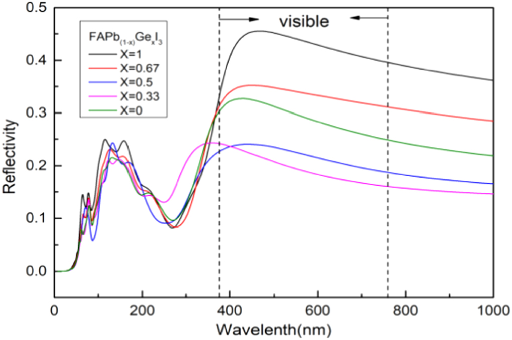
Standard image High-resolution imageThe C in above equation is a constant related to the Hall mobility of the electron, hν is the photon energy, Eg is the band gap width. With the increase of Ge's doping ratio, the band gap decreases, the absorption peak increases and the absorption coefficient increases. Figure 11 shows the spectral reflectivity of FAPb1−xGexI3. It can be seen from the figure that the reflectivity is in the intermediate state without doping. With the doping of Ge, the reflectivity decreases first and then increases. We know that as the material reflects more sunlight, the photoelectron transition decreases, resulting in a decrease in the photoelectric conversion efficiency. In order to improve the photoelectric conversion efficiency, both absorption and reflection must be considered. The absorption of solar photons by the material must satisfy the photoelectric effect equation:

Where h is the Planck constant, ν is the frequency of the incident light, wo is the work function (equal to Eg ). According to formula (6), the photon with energy hν less than Eg cannot be absorbed when it enters. When the energy hν enters much greater than Eg , the photon scatters with the lattice after the transition and converts into heat energy, which cannot be converted into carriers. Therefore, the band gap width must be appropriate to maximize the photoelectric conversion efficiency. Experimental studies have shown that the optimal band gap is between 1.3 and 1.4 eV, because this band gap can absorb all visible light and most near-infrared light of the Sun.

Figure 11. Spectral reflectivity of FAPb1−xGexI3(x = 0,0.33,0.5,0.67,1).
Download figure:
Standard image High-resolution imageTable 3. PDOS peak value of 5p orbital of I near Fermi surface in FAPb1−xGexI3.
| X = 0 | X = 0.33 | X = 0.5 | X = 0.67 | X = 1 | |
|---|---|---|---|---|---|
| pDOS(electrons/eV) | 52 | 86 | 83 | 45 | 42 |
In order to better analyze the relationship between the band gap and the doping concentration, the data points of the band gap in figure 8 were fitted as shown in figure 12. The functional relationship between the band gap and the doping concentration was obtained as follows:


Figure 12. The relationship between band gap Eg and doping concentration x.
Download figure:
Standard image High-resolution imageAccording to this functional relation, the range of doping concentration x is between 0.55 and 0.65 to obtain the optimal band gap. It can be seen that the photoelectric conversion efficiency of FAPbI3 can be improved after doped with Ge. So far, we haven't seen the experimental report of FAPbI3 doped with Ge, but there are a lot of theoretical researches. Such as: Diao et al calculated FAPbI3 doped with Cs, Ge and Sn by first- principles [25]. They found that when Pb was completely replaced by Ge, FAGeI3 would become an ideal photoelectric material to replace FAPbI3. Although the photoelectric performance of the former was slightly lower, the former was non-toxic. Tang et al doped Sn to MAPbI3/FAPbI3 to reduce the band gap to 1.30/1.40 eV and found that the Sn-doped MAPbI3 and FAPbI3 had the larger optical absorption coefficient and theoretical maximum efficiency, especially for Sn-doped FAPbI3 [40].
3.2.4. Conductivity and dielectric functions
It is known that the real part of the conductivity corresponds to the actual dissipation of energy. When electrons hit the lattice, they encounter resistance and transfer energy to the lattice, causing the lattice to vibrate and eventually dissipate energy in the form of joule heat. The imaginary part of the conductivity corresponds to the conversion of the energy of the electric field to the kinetic energy of the electron, which makes the electrons move in simple harmonic motion under the action of an external alternating electric field. Figure 13 shows that the incorporation of Ge changes the real and imaginary parts of the conductivity. When there is no doping, the conductivity is in the intermediate state. When doped with Ge, the real part of the conductivity first decreases and then increases, while the imaginary part of the conductivity first increases and then decreases. As the doping ratio increases, the bigger the real part is, the smaller the imaginary part is, which means more energy is lost. Therefore, the energy loss can be effectively regulated and the photoelectric conversion efficiency can be improved as long as the doping ratio of Ge is controlled.

Figure 13. Conductivity of FAPb1−xGexI3(x = 0,0.33,0.5,0.67,1).
Download figure:
Standard image High-resolution imageIn order to better understand the relationship between the photoelectron structure and the optical absorption coefficient, the linear optical properties of FAPb1−xGexI3 compounds will be discussed below according to the Kohn–Sham particle equation and Kramers-Kronig relation theory [1, 41]. Based on DFT, the frequency-dependent complex dielectric function can be expressed as follows:

In formula (8),  and
and  represent the real part and the imaginary part respectively, ω is the photon angular frequency. The real part can be obtained through the Kramers-Kronig relation:

In the above formula, M is the principal component value of the integral. The imaginary part is given by the Kohn–Sham particle equation:

Where e represents the charge of the electron, V is the volume of a single cell, p is the momentum transition matrix,  is the reduced Planck Constant.
  and
and  are the wave functions of VB and CB. The absorption equation can be expressed as follows:

The propagation behavior of electromagnetic fields in a material is described by the real part of the dielectric constant, while the absorption of light in the material is described by the imaginary part. The real and imaginary parts of the dielectric function of FAPb1−xGexI3 are shown in figure 14. It is clear from the figure that the real and imaginary parts of the undoped dielectric function are in the intermediate state. When doped with Ge, the real and imaginary parts of the dielectric function decrease first and then increase, because the dielectric function is inversely proportional to the width of the band gap. From figure 14, the real and imaginary parts of the dielectric function have two wave peaks, which are located near 200 nm and 500 nm respectively. This is consistent with the previous range of absorption peaks and the real part of the conductivity. It can also be seen from formula (11) that the absorption intensity is related to the dielectric function, so it is reasonable for them to peak at the same wavelength. As can be seen from figure 14, when the wavelength is about 450 nm, the doping ratio of FAPb1−xGexI3 with x = 1 appears negative. We know that a negative value means that light cannot travel to the perovskite material and that the material exhibits metallic luster. In figure 14, the two peaks of the imaginary part of the dielectric function are determined by electron transitions. Among them, the peak near 500 nm in visible light is determined by the shallow energy level transition of upper valence band to the lower band, while the peak near 200 nm in ultraviolet light is determined by the deep energy level transition of valence band to the conduction band. We find that when Pb is replaced by Ge, the peak value of the imaginary part of the dielectric function is the highest in the visible range among them, which indicates that it has the best dielectric performance and good photoelectric properties.

Figure 14. Dielectric function of FAPb1−xGexI3(x = 0,0.33,0.5,0.67,1).
Download figure:
Standard image High-resolution image
4. Conclusions
The band structure, DOS, charge density and absorption coefficient of FAPbI3 are calculated by the first-principles based on the DFT. It is found that the conduction band near the Fermi surface of the three structures is mainly contributed by the 6p orbital electrons of Pb, and their valence band near the Fermi surface is mainly contributed by the 5 P orbital electrons of I. The DOS of valence band near the Fermi surface of the tetragonal structure FAPbI3 is significantly higher, because its DOS of the 5p orbital electrons of I is significantly higher than that of the other two structures. The covalent interaction between Pb and I is relatively strong. Although the bond formed by FA is relatively weak, the main function of FA is to stabilize the structure. The super SOC effect of the heavy metal Pb element leads to the splitting of the conduction band level of FAPbI3, the conduction band value drops sharply, and the band gap decreases sharply. It is found from the spectral absorption coefficients of the three structures that the absorption peak of the tetragonal structure is in the visible light, and the absorption region of the near infrared is the largest. This indicates that the tetragonal structure of FAPbI3 is the structure with the best absorption coefficient.
It is found that doping with Ge can improve the photoelectric performance of FAPbI3. The incorporation of Ge mainly affects the conduction band, because the hybridization of Ge'4p orbital electrons and Pb'6p orbital electrons leads to the decrease of the conduction band and the reduction of the band gap. As the increase of doping ratio of Ge, the band gap gradually decreases. When all Pb are replaced, the band gap is only 0.849 eV. Therefore, the band gap width of the material can reach 1.3–1.4 eV of the optimal light-absorbing material of solar cell as long as the doping ratio of Ge is adjusted between 0.55 and 0.65. Doping with Ge will affect the flatness of conduction band and valence band of FAPbI3 and reduce the effective mass of electrons and holes. This is beneficial to the separation and transmission of photo-generated carriers, which can increase the short circuit current JSC and improve the photoelectric conversion efficiency of solar energy. The peak value of all indexes appeared at the same time around 200 nm and 500 nm, which was consistent, indicating that our research method was feasible. This study shows that doping with Ge can change the band structure and photoelectric performance of FAPbI3, which can provide certain reference for the experimental study of new high-efficient doped with organic-inorganic perovskite solar materials.
Acknowledgments
This work is supported by the National Natural Science Foundation of China Program (Grant No.11164004, 61835003) and the Industrial Research Project of Guizhou Province(GY[2012]3060).