
Abstract
A comparative study was done on three types of TiO2 thin film morphology, i.e., mesoporous nanoparticles, nanorods, and nanobranched nanorods thin films, as the scaffold for the perovskite solar cell. The performances of the perovskite-coated thin films were compared in terms of charge carrier extraction, charge transport, and solar energy harvesting via photoluminescence and UV–vis spectroscopies. TiO2 nanobranched nanorods thin film showed better photovoltaic performance than those of mesoporous nanoparticles and nanorods thin films. The better optical properties of nanobranched nanorods thin film as the scaffold is ascribed to its unique morphological advantages, i.e., remarkable specific surface area along with high-speed pathways for charge carriers. These characteristics lead to great, compact, and uniform perovskite loading, excellent electron transport property, and desired light harvesting performance, which are preferable features for promoting the efficiency of the perovskite solar cells. This paper introduces an outstanding scaffold for fabrication of high-performance perovskite solar cells.
Export citation and abstract BibTeX RIS

Original content from this work may be used under the terms of the Creative Commons Attribution 4.0 licence. Any further distribution of this work must maintain attribution to the author(s) and the title of the work, journal citation and DOI.
1. Introduction
High photovoltaic efficiency, low production cost, and easy fabrication by solution processes make inorganic halide perovskite solar cells (PSCs) the most promising candidate among various types of solar cells [1–8]. A typical PSC with a p-i-n junction configuration includes five layers. A light absorbent perovskite layer places between an n-type electron transfer layer (ETL) and a hole transport layer (HTL). ETL and HTL layers are generally TiO2 and p-type organic semiconductor (spiro-OMeTAD), respectively. At i–n and p–i interfaces, the separation of the photogenerated charges occurs through in situ electrical field. Photogenerated electrons and holes collect by the FTO and cathode (e.g., Ag) layers, respectively [9–13]. Inadequate light absorption, short diffusion lengths of charge carriers, and charge recombination are the most significant reasons for limited power conversion efficiency of solar cells [14]. High specific surface area and fast charge transport are preferable features for solar cells [15].
Mesoporous nanoparticles based scaffold provides large surface area but suffers from poor electron mobility. On the other hand, one-dimensional nanomaterials such as nanorods and nanowires represent rapid electron conducting. However, their low surface area compensates their favorable advantage. Due to their remarkable specific surface area along with high-speed pathways for charge carriers, three-dimensional (3D) hierarchical nanostructures are outstanding candidates for photoelectrochemical application [16–19]. Daneshvar e Asl and Sadrnezhaad [20] successfully synthesized TiO2 nanoleafed nanorods thin film, and evaluated it as a novel-designed photocatalyst for the photodegradation of anionic and cationic dyes. The improved photocatalytic performance of TiO2 is ascribed to large surface area and desirable light harvesting. Chen et al [21] reported a novel facile and one-step synthesis of hierarchical TiO2 nanotubes, and used this nanostructure in fabrication of the photoelectrode of the dye-sensitized solar cell. Considerable obtained efficiency of 9.89% is attributed to directed charge transport, excellent light harvesting, and effective charge collection. Li et al [22] successfully prepared stainless steel mesh-supported 3D hierarchical SnO2/Zn2SnO4 composite for gas sensor, solar cell, and photocatalysis applications. Xu et al [23] synthesized sheet-like CdS sensitized ZnO film by hydrothermal method. The photoelectrochemical property enhancement is ascribed to the improved light absorption and enhanced charge separation and transportation.
In this paper, TiO2 mesoporous nanoparticles, nanorods, and nanobranched nanorods thin films were synthesized and utilized as the scaffold for perovskite coating for further use in PSCs. The performance of the thin films were compared in terms of charge carrier extraction, charge transport, and solar energy harvesting through photoluminescence and UV–vis spectroscopies. Perovskite-coated TiO2 nanobranched nanorods thin film showed the best photovoltaic performance due to desirable characteristics of nanobranched nanorods thin film.
2. Experimental
2.1. Materials
Analytical-grade raw materials were bought from the following producers:
- (a)Fluorine-doped tin oxide (FTO) glass and TiO2 paste (18 NR-T) from Dyesol Company,
- (b)Titanium butoxide, titanium tetrachloride, acetone, ethanol, 2-propanol, hydrochloric acid, and sodium chloride from Merck, and
- (c)Titanium isopropoxide (TTIP), ammonium hexafluo-rotitanate, lead iodide, N,N-dimethylformamide (DMF), methylammonium iodide (MAI) powder, zinc powder, boric acid, and iso-propanol from Sigma-Aldrich.
2.2. Synthesis
A patterned FTO substrate was prepared via chemical etching with hydrochloric acid and zinc powder. TTIP was mixed with ethanol to make the solution precursor of compact TiO2 (C-TiO2) film. C-TiO2 film were coated on the patterned FTO by spin coating under 2000 rpm for 60 s followed by heating at 80 °C and 500 °C for 10 min and 30 min, respectively. Then, three types of TiO2 scaffold were deposited on the C-TiO2 film. Mesoporous nanoparticles (Meso) film was prepared by spin coating TiO2 paste diluted in ethanol with weight ratio of 1:7 under 4000 rpm for 30 s. Nanorods (NR) and nanobranched nanorods (NRNB) thin films were synthesized on top of C-TiO2 film via the hydrothermal and aqueous chemistry methods according to our previous work [24]. The coated TiO2 thin films were annealed at 450 °C for 30 min. For perovskite layer coating, a solution of lead iodide in DMF (1 M) with 70 °C temperature was spin coated on the TiO2 scaffold at 6500 rpm for 5 s, and dried at 100 °C for 30 min. Then, the layers were exposed to MAI powder in the oven with 150 °C temperature for 2 h. After cooling in ambient temperature, the layers were cleaned by iso-propanol, and then heated at 140 °C for 30 min. The synthesis procedure are summarized in Scheme

Scheme 1. Preparation procedure of perovskite layer onto different TiO2 scaffolds.
Download figure:
Standard image High-resolution image2.3. Instrumentations and characterizations
Morphological surface and cross-sectional images of bare and perovskite-coated TiO2 thin films were taken on a field emission scanning electron microscope (FESEM; MIRA3TESCAN-XMU). The composition and crystal structure of the layers were evaluated by the x-ray diffractometer (XRD) (X'Pert PRO MPD (PANalytical) with Cu Kα radiation). The light absorption characteristics of the perovskite layers on various TiO2 scaffolds were investigated by UV–Vis spectrophotometer (Avaspec-2048-TECwith AvaLamp DH-S Setup) with an integrating sphere attachment. Steady-state and time-resolved photoluminescence (Pl) of the perovskite layers were measured by Avaspec 2048 TEC spectrophotometer.
3. Results and discussion
FESEM analysis was employed to study the effect of TiO2 scaffold morphology on the quality of upper perovskite layer. It was thus possible to understand the correlation between crystal growth behavior and grain size with perovskite layer quality. FESEM images of three types of TiO2 thin film, i.e., Meso, NR, and NRNB, as well as perovskite layer coated on them are shown in figure 1. As it is clear in figures 1(a)–(c), TiO2 thin films are crack-free and monotonously covered the substrate surface. The trunk of NRNB structure could provide a fast charge pathway to improve electron collection and probably decrease hysteresis effect compared with Meso structure. In analogy with NR arrays, the 3D morphology of NRNB make much higher volume density available for the nucleation of perovskite layer. Moreover, this structure could increment the optical pathways through light scattering. Also, NBs present in the space between NRs could extract photogenerated electrons from MAPbI3 to overcome the hindrance of short electron diffusion length in the MAPbI3. Figures 1(d)–(f) shows surface images of perovskite layers prepared onto different TiO2 scaffolds. Perovskite layer formed on TiO2 NRNB is more compact and has fewer voids than those obtained by TiO2 Meso and NR scaffolds. This observation may be attributed to the slower rate of inter diffusion and reaction between the MAI vapor and the PbI2 film in presence of TiO2 NRNB. In both TiO2 NRNB and Meso, nucleation and growth of perovskite is greatly affected by the scaffold. The coating behavior of the perovskite layer is improved by using TiO2 NRNB. A perovskite capping layer with high coverage helps enhance light absorption and improve the performance of the solar cell. A large proportion of voids can be seen in perovskite layer that was processed by TiO2 NR. In this sample, there is a high probability of contact between the ETL and HTL. As a result, charge carrier species, i.e., electrons and holes, may recombine within the perovskite layer, and it decreases efficiency of the solar cell.
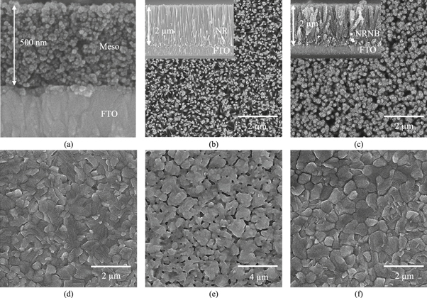
Figure 1. FESEM images of TiO2 (a) Meso, (b) NR, and (c) NRNB thin film and of perovskite layer coated on TiO2 (d) Meso, (e) NR, and (f) NRNB. The insets of (b) and (c) show images of the cross-sectional view of TiO2 NR and NRNB thin films.
Download figure:
Standard image High-resolution imageFor a complete study of the nature of perovskite layers coated on different TiO2 scaffolds, XRD analysis was employed (figure 2). Similarity in the XRD patterns between perovskite samples prepared on various TiO2 scaffolds indicates that all scaffolds produce the same perovskite. The 2θ values of 31.8°, 28.4°, and 14.1° are the main peaks for perovskite crystals. These values correspond to (310), (220), and (110) lattice planes of tetragonal perovskite crystalline structure, respectively [25–28]. Also, as pointed out in figure 2, a peak is observed at 12.7°, corresponding to the (001) lattice plane. This peak relates to the not-reacted PbI2. In other words, the conversion to perovskite is incomplete. The strongest peak for residual PbI2 is observed in perovskite layer with NR scaffold. The sample prepared in the presence of NRNB scaffold exhibits the weakest peak of PbI2, indicating a near complete transformation to perovskite. A large fraction of residual PbI2 in perovskite layer is expected to be harmful to the solar cell efficiency. This is mainly results from the electrical insulating nature of PbI2 [29, 30].

Figure 2. XRD patterns of perovskite layers coated on various TiO2 thin films.
Download figure:
Standard image High-resolution imageTo determine the optical properties of perovskite layers deposited on various TiO2 thin films, UV–vis absorption spectra were acquired. The absorption range from 400 nm up to 750 nm is shown for all prepared layers in figure 3, which indicates the formation of perovskite on the TiO2 scaffolds. The UV–vis absorption is initially improved in presence of TiO2 NRNB scaffold. Generally, full coverage and compact perovskite layer can increase the UV–vis absorption [31, 32], which can approve the highest UV–vis absorption for perovskite layer deposited on top of TiO2 NRNB scaffold. A decline in the light absorption is seen for the TiO2 NR-based perovskite layer, which derives from the partially coverage of perovskite layer with higher voids.

Figure 3. UV–Vis absorption spectra of perovskite layers coated on different TiO2 thin films.
Download figure:
Standard image High-resolution imageTo comprehensive study of the optical properties of perovskite layers, Pl spectrums of the perovskite-TiO2 films were measured. In general, the charge carrier extraction in the perovskite layer is mainly dependent on the perovskite layer morphology. Figure 4(a) displays the steady-state Pl spectrums of perovskite layers deposited on different TiO2 films. The Pl intensity decrease indicates effective charge carrier extraction happens within the perovskite-TiO2 films [33–35]. The higher Pl intensity of perovskite-TiO2 NR is resulted from an inhomogeneous perovskite layer with a high number of voids. A low Pl intensity can be seen for perovskite-TiO2 NRNB, that is attributed to high coverage and compactness of perovskite layer. Thus, the steady-state Pl analysis indicates that the high charge carrier extraction efficiency occurs in the uniform and smooth perovskite layer. To study the charge carrier extraction/transfer behavior, the time-resolved Pl decay spectra of different perovskite-TiO2 films were measured, as presented in figure 4(b). The shortest Pl decay lifetime can be seen for the perovskite-TiO2 NRNB scaffold, which shows the faster charge carrier transfer into ETL and HTL. An efficient and fast charge carrier extraction and transfer process into charge carrier layers results from the compact and unharmed perovskite layer-TiO2 scaffold interface. An inhomogeneous and partially coverage perovskite layer with voids can provide recombination sites, which leads to an insufficient charge carrier extraction/transfer. The Pl decay lifetimes for the perovskite layers prepared onto different TiO2 scaffolds were 14.11, 17.21 and 19.99 for TiO2-NRNB, TiO2-Meso, and TiO2-NR, respectively. It is well-known that the charge carriers generated in the perovskite domain can be injected into ETL, and the PL of perovskite layers occurs due to the recombination of localized charge carriers. The spectrum of perovskite layer prepared with TiO2-NRNB substrate shows a significant depressed PL (14.11 ns) compared with that of the layers with TiO2-Meso and TiO2-NR (17.21 ns and 19.99 ns, respectively), indicating that the charge carriers generated can be effectively generated and extracted. In fact, the diffusion length of charge carriers is increased by 21% and 40% in presence of TiO2-NRNB substrate compare with TiO2-Meso and TiO2-NR, respectively.

Figure 4. (a) Steady-state and (b) time-resolved Pl spectrums of perovskite layers coated on different TiO2 thin films.
Download figure:
Standard image High-resolution image
4. Conclusions
Three types of TiO2 thin film, i.e., mesoporous nanoparticles, nanorods, and nanobranched nanorods, were synthesized and used as the scaffold for perovskite coating for further use in the perovskite solar cell. Hierarchical nanobranched nanorods thin film presented better optical properties compared with thin films of mesoporous nanoparticles and nanorod arrays. In fact, the large surface area and charge transport property of nanobranched nanorods led to uniform and compact perovskite loading, excellent electron collection, and desired light harvesting performance, which are preferable features for promoting the efficiency of the perovskite solar cells.
Acknowledgments
This work was partially supported by the Iran National Science Foundation.
Conflicts of interest or competing interests
The authors declare that they have no known competing financial interests or personal relationships that could have appeared to influence the work reported in this paper.
Data availability
The data that support the findings of this study are available upon request from the authors.