

Abstract
Manipulations of light–matter interaction via sub-wavelength plasmonic structures have opened up many new research opportunities in photonics from microwave to the visible spectrum, including the relatively underdeveloped but technologically important terahertz regime. Here, we have studied manipulation of terahertz transmission through a bilayer metasurface consisting of a metallic hole array and a complimentary patch array separated by an ultra-thin dielectric spacer. The terahertz transmission spectra through our studied metasurfaces exhibit characteristic resonances due to the surface plasmon induced extraordinary transmission peak. Our study reveals a counterintuitive blue shift of the transmission peak with increasing spacer thickness, which is explained by reduced Coulomb interaction between two plasmonic layers. The measured quality factor exhibits a strong dependence on the spacer thickness, and the maximum quality factor is observed for a spacer thickness of around λ/30, indicating strong electric-field confinement inside the dielectric spacer. These bilayer plasmonic structures will aid in realizing next-generation terahertz plasmonic devices such as ultrasensitive thin-film sensors, modulators, narrow-band filters, and other nonlinear components.
Export citation and abstract BibTeX RIS
1. Introduction
Since its first demonstration, extraordinary transmission (EoT) through sub-wavelength hole arrays has garnered immense research interest [1–5]. In most works, EoTs are attributed to the excitation of surface plasmons on the metal-dielectric interface, which mediate through sub-wavelength holes and then radiate back to free-space. Generally, the transmission efficiency of such hole arrays is orders of magnitude higher than the transmission predicted by the general aperture theory [6–9], a phenomenon which has been widely exploited across a multitude of applications [10–19]. In the terahertz domain, surface plasmon assisted EoT has remained an area of active research over the years for its applications in various fields including biomedical sensing [10, 11], active modulators [12–14], filters [15], switches [16–19], etc.
Various techniques to manipulate EoTs in subwavelength metallic hole arrays have been proposed and demonstrated over the last few decades. In 1999, Kim et al evidenced controlling of EoTs by changing hole geometries, the refractive index of the surrounding medium, and the angle of incidence of the incident radiation [20]. Adding circular grooves around the holes [21], or designing coaxial apertures [22], were found to enhance the magnitude of the transmissions substantially. Structures similar to metal-semiconductor Schottky diodes were demonstrated to possess electronic control capabilities over the EoTs [14]. Additionally, hole arrays integrated with back-gated graphene films [23] and hole arrays on superconductive thin-films [13] were employed to control the EoT induced transmission amplitude and frequency in a dynamical manner.
The terahertz spectrum (0.1–5 THz) has in recent times proved to be increasingly useful in a variety of emerging fields due to the fact that a majority of substances, both organic and inorganic, display unique resonant signatures in this domain, which can be exploited for label-free non-intrusive detection and identification of these materials [24, 25]. Plasmonic metasurfaces, have acted as great facilitators for making practical applications of the unique properties of the THz spectrum a reality [26–29], especially in the domain of THz plasmonics [30, 31]. In this context, near field coupled metasurfaces provided additional degree of freedom with the capability of controlling terahertz transmissions efficiently [32, 33]. In another work, Pattanayak et al[ 34] demonstrated that resonance peaks and Q factors of transmitted bands can be controlled using a periodic array of asymmetric apertures by switching the polarization of incoming THz waves. Recently, rectangular hole arrays filled with extreme uniaxial metamaterials numerically demonstrated to produce an extensive increase in transmission amplitude due to the Fabry–Perot effect [35]. Therefore, in recent times significant efforts are being dedicated to manipulate EoT effects through complex meta structures. Motivated to manipulate EoT transmissions, in this work we have explored near field coupled sub-wavelength metastructures by pairing patch resonators with their complementary hole arrays. Our work demonstrated that controlling the inter resonator near field electromagnetic coupling between the upper resonator and lower hole array can lead to polarization independent controllability on extraordinary terahertz transmissions. Unlike typical single layer hole arrays, this scheme is capable of confining stronger electromagnetic fields inside a deep sub-wavelength ultrathin spacer region, and hence can lead to strong light-matter interactions, ultrasensitive sensing, narrow band filter, nonlinear effects, etc.
We have designed, fabricated, and characterized the proposed hybrid metasurfaces. Our metasurfaces consist of two metal films with sub-wavelength dimensions. The bottom layer contains an array of square-shaped holes on an undoped silicon substrate; the top layer is an array of sub-wavelength square patches (exactly complementary structure), and they are separated by an ultra-thin dielectric spacer (figure 1). The transmission characteristics of this hybrid structure have been investigated using terahertz time-domain spectroscopy (THz-TDS) [36, 37]. We have validated our experimental results through extensive numerical simulations using the commercially available numerical software, CST Microwave Studio. The experimental data agree well with the simulation results, and therefore validate our studies on these hybrid metastructures.
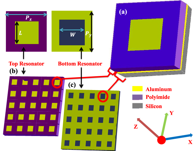
Figure 1. (a) Schematic of a unit cell of the hybrid structure along with the decoupled (b) top resonator array and (c) bottom hole array. The hole array comprises of aluminum (yellow) on silicon (grey) substrate, while the top resonator array consists of aluminum (yellow) on polyimide spacer (magenta). The geometric parameters are L, W( where L= W, dimensions of the square holes and resonators), and Px = Py( the periodicities in the x and y directions, respectively).
Download figure:
Standard image High-resolution image2. Fabrications, testing, and simulations
Several sets of the sub-wavelength structures were fabricated using typical micro fabrications, involving standard photolithography, metallization, and lift-off. To understand the intrinsic response of independent layers, we also fabricated the intrinsic (uncoupled) bottom hole array on a high resistivity silicon wafer. The top resonator array (square metallic patch) was fabricated on a polyimide coated high resistivity silicon substrate. Additionally, we fabricated four different samples on silicon substrates, containing both of the sub-wavelength plasmonic layers, which were separated by a polyimide spacer of different thicknesses. The plasmonic layers were overlaid carefully so that the square holes were aligned perfectly with the square patches. Figure 2 shows optical images of one of the fabricated hybrid samples, along with the decoupled samples.
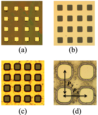
Figure 2. Optical images of the fabricated metastructures: (a) decoupled top resonator array, (b) decoupled bottom resonator array, (c) coupled dual layer hybrid structure array, and (d) magnified view of coupled hybrid structure.
Download figure:
Standard image High-resolution imageThe periodicity of the unit cell for all the samples was fixed at 80 μm (Px = Py = 80 μm) (figure 1). The dimension of the square hole (W) is exactly equal to the dimension of the square patch (L) with a value of W= L=40 μm. For the decoupled samples, the hole array and patch resonator array were fabricated on identical silicon substrates. Electron beam evaporation was used to deposit aluminum of thickness 200 nm, and subsequently, typical lift-off in acetone bath was employed to realize the desired arrays. For the coupled structures, thin films of polyimide spacers of varying thicknesses were spin-coated onto the fabricated hole arrays, which were hard baked using slow annealing steps from room temperature to 220 °C to ensure uniform thickness of the spacer layer over the array surfaces. After careful aligning, similar photolithography, metallization and lift-off procedures were carried out to realize the square-shaped complimentary resonator array atop the spacer layer, thus completing the coupled structure.
All the samples were characterized using a photoconductive antenna based (InGaAs/InP) THz-TDS, where a femtosecond laser (1560 nm, 100 MHz, ∼60 fs) is used to generate terahertz pulses using the Teraflash THz source (Toptica Photonics). The detector and emitter contain a 25 μm dipole antenna and a 100 μm strip-line antenna, respectively, both of which consist of InGaAs/InP photoconductive switches [36]. The transmitted THz pulses through the samples were detected in the time domain using the pump probe principle. A blank piece of identical silicon substrate was used as a known reference material and transmitted THz pulses through the blank substrate were used as reference signals. The time-dependent terahertz pulses were then converted to the complex frequency spectra using fast Fourier transformation. To obtain the amplitude transmission of a sample, the spectrum transmitted through the sample was normalized with the spectrum transmitted through the reference. All the transmission measurements were carried out at room temperature in a dry environment.
Our experimental results have been validated using commercially available full-wave numerical simulator CST Microwave Studio. The frequency domain solver in CST has been used to numerically simulate the intrinsic (decoupled) hole and resonator array, as well as the hybrid structures with varying spacer thicknesses. We used tetrahedral meshing for the simulation with a periodic boundary condition to increase accuracy while reducing the required computational time. The wave vector of the incident wave is set normal to the plane of the metamaterial array. We have chosen a Floquet port along with an adaptive mesh configuration in the numerical simulations to solve Maxwell equations to compute the transmitted spectra numerically. The dielectric properties of polyimide and silicon were set to  and
and , respectively, in our simulations [38–40].
3. Observations and discussions
3.1. Transmission properties
In this section, we examine the transmission properties of the hybrid structure for polarization independent incident THz waves. Firstly, we have measured the transmission properties of the decoupled top and bottom hole array independently and then compared these experimental results with those obtained from our simulations. As can be seen from figure 3, the experimental results are in good agreement with the simulations. As depicted in figure 3(a), the top resonator array shows typical dipole resonant behavior for THz transmissions with a broad transmission drop at around 1 THz. In figure 3(b), the bottom hole array shows a transmission peak at around 1 THz, followed immediately by a dip at around 1.05 THz, and another dip at around 1.45 THz, which can be attributed to Wood's anomaly [41, 42]. The transmission peak at 1 THz is due to the excitation of surface plasmon induced resonance [1–5].
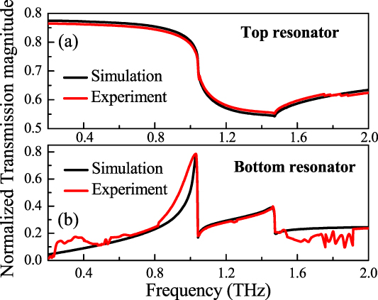
Figure 3. Simulated and experimental normalized transmission responses of (a) decoupled top resonator array and (b) decoupled bottom hole array.
Download figure:
Standard image High-resolution imageIn order to understand the effects of coupling between two near field plasmonic layers, we have pursued a second set of experiments where we varied spacer thicknesses to 2.04 μm, 2.78 μm, 3.35 μm, and 5.92 μm, respectively. The resulting transmission plots are shown in figure 4. For a systematic comparison, experimental data (figure 4(a)), along with the numerical simulations (figure 4(b)), are shown side by side. The comparison clearly reveals that our numerical simulations follow the same trend as the experimental observations. The ripples appearing in the experimental observations (figure 4(a)) beyond 1.5 THz can be attributed to the limited bandwidth and system noise of our THz system. In order to avoid such noises masking the actual response of hybrid metastructures, we have deliberately designed the EoT resonances around 1 THz.

Figure 4. Comparative (a) experimental and (b) simulated plots of normalized transmission magnitudes versus frequency of the coupled structures for four different spacer thicknesses.
Download figure:
Standard image High-resolution imageThe EoT peak appears at 0.949 THz for a dielectric separation of 2.04 μm. As the separation increases, peaks keep moving towards the higher frequencies. As indicated in figure 4, for a spacer thickness of 2.87 μm, 3.35 μm, and 5.92 μm, the peak appears at 0.977 THz, 0.984 THz and 0.995 THz, respectively. A total of 46 GHz blue shift of the EoT peak along with a 0.173 alteration in peak transmission was observed for a spacer thickness change of 3.88 μm.
Based on the good agreement between simulations and measurements, we have further extended our study to include simulated responses of the hybridized structures with spacer thicknesses from 0.1 to 24 μm. The increase in transmission amplitude is observed to saturate around 24 μm of spacer thickness. Figure 5(a) shows the transmission curves of the entire range of thicknesses. It is worth noting that the EoT peak frequencies blue shift and transmission peak amplitudes increase with increasing spacer thicknesses.
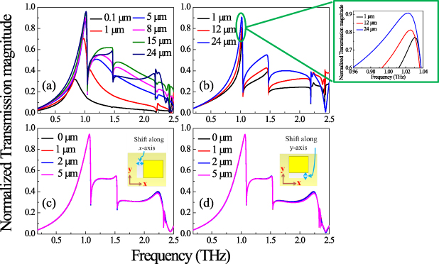
Figure 5. (a) Simulated normalized transmission responses as a function of spacer thicknesses ranging from 0.1 μm to 24 μm. (b) Simulated normalized transmissions through an identical intrinsic hole array with three different polyimide layer thicknesses (1, 12, and 24 μm). The inset of (b) shows the expanded view of the resonant peaks. (c), (d) The effects of misaligning the top resonator with the bottom hole array along the x and y axes, respectively, in progressions of 1 μm, 2 μm and 5 μm for a polyimide thickness of 24 μm.
Download figure:
Standard image High-resolution imageThe nature of the peak frequency shift is investigated in more detail. Figure 5(b) shows the transmission peaks for an intrinsic bottom hole array with polyimide overlayers. The EoT peak shows redshift with increasing overlayer thickness. Such redshifts in the transmission peak occur because of the increased effective dielectric constant, similar to works demonstrated earlier [43]. As polyimide is progressively deposited on top of the hole array, it first fills the holes in the array structure and eventually forms a dielectric overlayer, which can be equivalently described as increasing capacitance [43]. This enhanced capacitance can 'store' energy in the form of electromagnetic fields. The process described above leads to an effective increase in the net capacitance of the metastructure, which shifts the resonance peak progressively towards the lower side of the frequency spectrum. Comparing the same spacer thickness with and without the top resonator, we noticed that in figure 5(a) extraordinary peak frequencies of the hybridized metastructures blue shift compared to the peak frequencies of the intrinsic hole arrays with similar spacer thicknesses
We have numerically investigated the effect of misalignment between top and bottom metallic layers. We chose a polyimide thickness of 24 μm and progressively misaligned the resonator along x-axis and y-axis as shown in figures 5(c) and (d), respectively. For both orientations, we introduced a misalignment of 1 μm, 2 μm and 5 μm from the perfectly aligned position. Our simulated results show that the frequency shifts and changes in transmission magnitude due to the misalignments are negligible. This is true for all other spacer thicknesses; therefore, we have continued further studies considering the resonator and the hole perfectly aligned.
To effectively explain the nature of the trends in transmission responses observed in figures 5(a) and (b), we have probed into the nature of the interlayer coupling between the top resonator and the bottom hole array, as shown in figure 6(a). Figure 6(a) reveals that the electric field induces opposite charges on the same edges of both the top resonator and the bottom hole, which attract each other due to the Coulomb interaction effect [44], setting up a pattern of constructive interference between the layers. The electromagnetic interferences between the different layers in the metastructure, which aid in increasing the amount of electric field confinement within it, are considered here as constructive interferences. Any interference, on the other hand, which inhibits further electric field confinement, is considered destructive. The constructive interference described above, aids in containing the fringing electric fields in the spacer layer. The attractive Coulomb force between opposite charge polarities increases the effective capacitance. As the thickness of the polyimide layer increases, the effective capacitance decreases due to reduced Coulomb attraction, and the blue shift of the EoT resonance peaks (figure 5(a)) saturates beyond a certain spacer thickness.

Figure 6. (a) Side view of a unit cell of the hybrid metastructure showing the directional electric field lines between the top resonator and the bottom hole array. For clarity, the induced charge centers are indicated in the figure. (b) Q factor and normalized transmittances of the hybrid metamaterials with varying spacer thicknesses. Experimentally obtained data points are marked with red circles. The maximum Q factor of 10.85 is observed at around 8 μm spacer thickness.
Download figure:
Standard image High-resolution imageOn the other hand, when the spacer thickness is lower, the strong Coulomb attraction between the resonator and the hole arrays actually acts as an inhibitor for the surface plasmon polaritons (SPPs) traveling along the upper surface of the hole array. Since these SPPs eventually are responsible for the EoT peaks, their inhibition results in lower amplitude of the resonance peaks when the resonator and the hole arrays are very close to each other. As the spacer thickness increases, the strength of the constructive coupling between the two metal layers keeps decreasing, and this, in turn, results in higher transmission peaks. However, beyond a certain thickness (observed to be around 8 μm), the coupling weakens largely. As a result, we observe a trend towards saturation in the amplitude of the EoT resonance peaks.
Another interesting phenomenon observed in the course of our study is related to the amplitude of the dip immediately after the EoT peak. While it is almost negligible at lower spacer thicknesses, it increases with increasing spacer thickness. This can be explained by the redistribution of energy from the 'passing off' orders of the diffracted THz beam to the 'allowed' orders [41, 45]. Taking a cue from the previous paragraph, as the inhibiting influence of the interlayer Coulomb attraction on the resultant field generated due to the interaction between the resonator fields and the incident wave coupled with the SPPs from the hole array decreases with increasing spacer thicknesses, more energy from the 'passed off' orders are redistributed to the 'allowed' orders, aiding in increasing the amplitude of the EoT peak and leading to sharper and more defined Wood's anomaly generated dips. The same principle applies to the Wood's anomaly dips occurring at higher frequency modes too (around 1.5 THz, 2.2 THz, 2.4 THz) seen in figure 5(a).
3.2. Q factor
We have further studied the performance of the hybrid metamaterials by evaluating the quality factors (Q), which is the ratio between the resonant frequency and its corresponding full-width at half-maxima. Q factor along with normalized transmittances for several spacer thicknesses is plotted in figure 6(b). The data points obtained from our experimental observations are marked as red rings in figure 6(b). It can be observed that the experimental observations match well with the numerical simulations, and therefore we proceed with further investigations to study the fabricated structures.
Peak transmittance amplitude initially increases rapidly with increasing spacer thickness, and then it slowly saturates. On the other hand, Q factor increases initially with increasing spacer thickness, until it reaches a maximum of ∼11 for a spacer thickness of 8 μm, then decreases with the further increase of spacer thickness. We attribute the interlayer near field constructive coupling between the resonators and hole arrays due to Coulomb attraction and the electric field confinement in the spacer, for such a variation in Q factor with respect to spacer thicknesses. As the spacer thickness increases, constructive interferences between the electromagnetic fields generated at the top resonator and the bottom hole array decreases, leading to decreased inhibition on SPP movement and stronger fringing field confinement inside the spacer layer. Because of this effect, the Q factor initially increases until the spacer thickness becomes ∼8 μm, as observed in figure 6(b). Beyond this thickness, the near field coupling strength reduces with further increase in spacer thickness, leading to the restoration of uncoupled SPP oscillation. The electric field in the spacer also reaches maximum confinement capacity around the same thickness. Both of these factors contribute to a subsequent monotonous decay in the Q factor.
3.3. Electric field profile
To further confirm our understanding of the inter-related physical mechanisms described previously, we have studied the induced electric field profiles at the resonant peaks for different spacer thicknesses. In figures 7(a)–(c), induced electric field profiles are observed on the top surface of a unit cell of the metastructure, since the fringing fields generated from the hole structure finally impinge on the resonator, and the SPPs are also generated on the top surface. Three different spacer thicknesses were chosen in order to probe weakly coupled (1 μm), strongly coupled (8 μm) and moderately coupled (24 μm) regimes, respectively. Strong electric field confinement in the spacer region is observed at 8 μm spacer thickness as compared to 24 μm and 1 μm. The maximum E field value (abs) is observed to be 3.36 × 10⁶ V m−1 inside the spacer region at 8 μm spacer thickness. This again proves our argument derived from the Q factor trend as seen earlier (figure 6(b)) and can be attributed to near field coupling between the electromagnetic fields induced in the top resonator and bottom hole array and fringing field confinement in the spacer. Energy confinement in the dielectric is weakest at 1 μm (figure 7(a)) due to inadequate spacer thickness to envelope the fringing fields and the dominance of inter-layer inhibitive interferences in SPP coupling, reaching a maximum at 8 μm (figure 7(b)). It then progressively decreases to an intrinsic value with increasing dielectric thickness, as is observable at 24 μm (figure 7(c)). The electric field enhancement plot in figure 7(d) follows this trend with enhancement factors of 6.6, 13.9, and 10.8 with respect to the incident electric field, for polyimide thicknesses of 1 μm, 8 μm and 24 μm, respectively, confirming our understanding of the various phenomenon occurring within the studied metastructure.

Figure 7. Electric field profiles for (a) 1 μm, (b) 8 μm and (c) 24 μm spacer thickness of our metastructure. Electric field confinement in the spacer is clearly higher in the case of spacer thickness 8 μm (b) compared to 1 μm (a) and 24 μm (c) cases. This is further supported through the electric field enhancement plot shown in (d). E field enhancement points corresponding to 1 μm, 8 μm and 24 μm have been circled in blue.
Download figure:
Standard image High-resolution image
4. Conclusions
In conclusion, we have demonstrated a hybrid metastructure consisting of a subwavelength hole array perfectly aligned with a complimentary patch-resonator array. We have demonstrated that modifying the spacer thickness between the two resonator layers can influence the EoT induced resonance amplitude as well as frequency. Our experiments are well supported by numerical investigations. We have further studied both Q factor and the electric field distributions at the EoT resonances. Our study demonstrates the maximum Q factor at a spacer thickness of 8 μm, equivalent to one-thirtieth of the operating wavelength. The demonstrated strong field confinement at deep sub-wavelength length scale indicates the utility of our vertically stacked plasmonic metastructures. Such strongly coupled multilayer metastructures can form the basis for future terahertz plasmonic devices.
Acknowledgments
S B acknowledges partial support from Department of Science & Technology (DST), project EMR/2015/001339. D R C acknowledges partial support from Department of Science & Technology (DST), project CRG/2019/001656. D K acknowledges assistance from Department of Science & Technology (DST) INSPIRE doctoral research fellowship, Ministry of Science and Technology, Government of India. A K A acknowledges support from the Los Alamos National Laboratory LDRD Program and the Center for Integrated Nanotechnologies, a US Department of Energy, Office of Basic Energy Sciences Nanoscale Science Research Centre operated jointly by Los Alamos and Sandia National Laboratories.