Fabrication and Characterisation of 3D Diamond Pixel Detectors With Timing Capabilities
 Lucio Anderlini1*
  Marco Bellini2 Andrea Bizzeti1,3
  Alessandro Cardini4 Roberto Ciaranfi1 Chiara Corsi5 Michela Garau4,6
  Adriano Lai4 Stefano Lagomarsino1 Andrea Lampis4,6 Angelo Loi4 Chiara Lucarelli1,7 Saverio Mariani1,7
  Nicola Minafra8
  Arianna Morozzi9 Roberto Mulargia10,11 Giovanni Passaleva1 Daniele Passeri9,12 Silvio Sciortino1,2,7 Stefania Vecchi13
  Michele Veltri1,14
- 1Istituto Nazionale di Fisica Nucleare–Sezione di Firenze, Firenze, Italy
- 2Istituto Nazionale di Ottica, Consiglio Nazionale delle Ricerche, Firenze, Italy
- 3Dipartimento di Scienze Fisiche, Informatiche e Matematiche, Università degli Studi di Modena e Reggio Emilia, Modena, Italy
- 4Istituto Nazionale di Fisica Nucleare–Sezione di Cagliari, Cagliari, Italy
- 5Laboratorio Europeo Spettroscopie Non Lineari, Sesto Fiorentino, Italy
- 6Dipartimento di Fisica, Università degli Studi di Cagliari, Cagliari, Italy
- 7Dipartimento di Fisica e Astronomia, Università degli Studi di Firenze, Firenze, Italy
- 8Department of Physics and Astronomy, College of Liberal Arts and Science, The University of Kansas, Lawrence, KS, United States
- 9Istituto Nazionale di Fisica Nucleare–Sezione di Perugia, Perugia, Italy
- 10Istituto Nazionale di Fisica Nucleare–Sezione di Genova, Genova, Italy
- 11Dipartimento di Fisica, Università degli Studi di Genova, Genova, Italy
- 12Dipartimento di Ingegneria, Università degli Studi di Perugia, Perugia, Italy
- 13Istituto Nazionale di Fisica Nucleare – Sezione di Ferrara, Ferrara, Italy
- 14Dipartimento di Scienze Pure e Applicate, Università degli Studi di Urbino, Urbino, Italy
Diamond sensors provide a promising radiation hard solution to the challenges posed by the future experiments at hadron machines. A 3D geometry with thin columnar resistive electrodes orthogonal to the diamond surface, obtained by laser nanofabrication, is expected to provide significantly better time resolution with respect to the extensively studied planar diamond sensors. We report on the development, production, and characterisation of innovative 3D diamond sensors achieving 30% improvement in both space and time resolution with respect to sensors from the previous generation. This is the first complete characterisation of the time resolution of 3D diamond sensors and combines results from tests with laser, β rays and high energy particle beams. Plans and strategies for further improvement in the fabrication technology and readout systems are also discussed.
1. Introduction
The development of the particle detectors for future hadronic machines, such as the High-Luminosity Large Hadron Collider (HL-LHC) at CERN, faces the major challenge of reconstructing the trajectories (tracks) of an unprecedented density of charged particles. State-of-the-art spatial granularity in the measurement of the energy deposits (hits) will be barely sufficient to distinguish tracks, and good time resolution will be necessary to distinguish the many hadronic collisions, or primary vertices, originated in a single bunch crossing [1, 2]. Time information has been demonstrated to be very beneficial in pattern recognition procedures especially in events with a large number of tracks, allowing for complete 4D tracking algorithms, possibly implemented on programmable gate array devices [3].
The time resolution of a detector is defined by three main contributions: variations of the shape of the signal due to inhomogeneities in the charge generation and collection mechanisms; a time walk contribution related to the signal processing technique; and a jitter contribution due to the electronic noise superposed to the signal (see, e.g., Ref. [4] for a more detailed discussion).
The development of silicon pixel detectors aiming at excellent resolution on timing measurements has been extremely active in recent years, mainly focusing on Low-Gain Avalanche Detectors (LGADs) [5, 6]. Best time resolutions are obtained with extremely thin LGAD sensors exploiting multiplication in a heavily doped 1–2 μm thick layer. Indeed, by reducing the thickness of the LGAD detectors, the contribution from Landau fluctuations can be reduced preserving good signal-to-noise ratio by means of charge multiplication. For example, time resolutions of the order of 30 ps per layer have been reported using 50 μm LGAD detectors [7].
The higher density of ionising particles expected at future experiments also represents a serious concern for the radiation damage of both sensors and front-end electronics. For example, the sensors in the innermost part of the vertex detector of the upgraded LHCb experiment planned for taking data from 2032 on, will have to cope with a radiation dose of the order of
Recently, a new generation of 3D silicon pixel detectors, with distances between the electrodes of few tens of micrometers, have been demonstrated to be resistant to radiation fluences up to
Since the spread in the collection time is strictly related to the carrier drift velocity, and therefore to the semiconductor material, an interesting area of research on timing pixel sensors consists in the study of semiconductors other than silicon. In particular, diamond is extensively studied for it combines high carrier velocity with an excellent radiation resistance, which is further improved when a 3D design is adopted to reduce the drift path [13–17]. Differently from the silicon devices, where the electrodes are obtained with micromachining and doping, in diamond sensors the electrodes are usually obtained focusing a femtosecond laser within the diamond bulk to induce a local phase transition to an ohmic mixture of diamond-like carbon, amorphous carbon and graphite [18, 19]. Recently, the single-hit efficiency of 3D sensors constructed with poly-crystalline chemical vapour deposition (CVD) diamond has been measured in a beam test using a high precision tracking telescope and found to be above 99% for particle fluxes up to 20 MHz/cm2
The high intrinsic break-down voltage allows operating diamond sensors with high electric field which, in combination with the high electron and hole mobility, may result into negligible contribution from the charge collection mechanism to the time resolution of 3D diamond detectors.
With Landau fluctuations limited by the 3D geometry and the spread in the collection time reduced because of the semiconductor material properties, it is reasonable to expect the jitter to dominate the time resolution. The slope of the output signal is directly affected by the time constant of the sensor which can be approximated by the product of the sensor capacitance by the resistance at the input of the amplifier. While the former is significantly smaller than in typical silicon sensors because of the thinner electrodes and smaller dielectric constant, the combination of diamond-like carbon, amorphous carbon and graphite constituting the electrodes makes the resistance at the input of the amplifier several orders of magnitude larger than in silicon detectors [21]. Higher resistance of the electrodes also results into an increase of the Johnson noise and therefore into larger jitter contributions to the time resolution.
In this work, we describe the design, the fabrication and the characterisation of timing 3D diamond sensors, with electrodes obtained through a pulsed laser graphitisation technique improved by the application of adaptive optics to reduce the electrode resistance. Following this introduction, Sections 2 and 3 describe the design and fabrication process, while Section 4 presents the characterisation of the sensor response to laser-induced excitations, β rays from 90Sr and minimum-ionising pions. Throughout the paper, a right-handed coordinate system is adopted, with the z axis parallel to the electrodes and the y axis along the vertical.
2. Simulation
The sensors described in this paper are top-quality single-crystal CVD (sCVD) diamond specimens [22, 23]. The
The pixel pitch is fixed to 55 μm × 55 μm to ease the comparison with silicon sensors compatible with the Timepix readout chip [24], while all other geometrical and physical properties of the sensors were optimised in terms of time resolution by taking advantage of various simulation approaches and experimental tuning campaigns.
2.1. Qualitative Considerations on the Detector Design
A simplified description of the sensor, modelling the charge collection by the resistive electrodes and the signal relaxation due to the readout electronics, is used to assess the dependence and the relative importance of the design parameters. The resistive electrodes are modeled as infinitely long columns arranged in rectangular elementary cells, as depicted in Figure 1A, on the left. The same figure also shows that the readout electrodes, which are usually virtually grounded by the amplifier, are interleaved with polarization electrodes. To simplify the numerical computation, the electric field is assumed to be stationary during the whole process of charge collection. Also the variation of the polarisation bias due to the signal current was neglected. With this approximation, the detector response can be described by a simple two-dimensional model as an application of the Ramo theorem [25]. The 2D representation of the elementary cell used for the simulation is depicted on the central panel in Figure 1B.
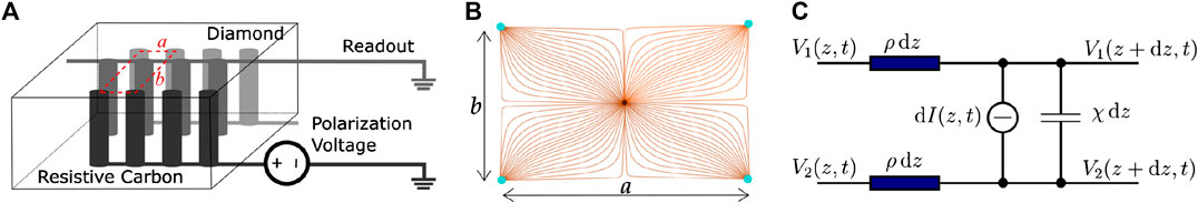
FIGURE 1. (A) schematic representation of the generic 3D
The capacitance of the cell and the resistance of the electrodes are relevant to the propagation of the electrical signal to the input of the readout electronics. A pair of electrodes is modelled as a resistive-capacitive line as illustrated in Figure 1C, on the right. The length of the line, and therefore the effect of the line on the signal, depends on the depth at which the charge is generated, providing a third spatial dimension to the description of the sensor.
The resistivity and thickness of the columns, the size of the elementary cell and the inclination of the traversing particles with respect to the sensors are all parameters whose effect can be studied, at least qualitatively, with such a simplified model. In addition, the simulation indicates that larger signals can be obtained connecting the readout and polarization electrodes on the opposite sides of the diamond sample, rather than connecting them to the same side (see Figure 1A).
The simulation also confirms that for higher bias voltages, and therefore higher electric field, the signals are faster and the time resolution improves. The benefit from an increase in the electric field beyond charge carrier velocity saturation is however marginal with respect to lowering the time constant of the charge relaxation process. The order of magnitude of the time constant is fixed by the product of the capacitance of the single cell and the resistance of the electrodes. The capacitance is defined by the size of the elementary cell and by the diameter of the columns. The resistance depends on the quality of the fabrication procedure and, quadratically, on the diameter of the columns.
Small elementary cells are necessary to achieve the spatial granularity required by tracking applications at future large-scale particle detectors. They improve the radiation resistance of sensors as well as their time resolution due to the shorter charge carrier transit time. However, smaller elementary cells result into larger capacitance putting stronger requirements on maximum electrode resistivity.
Finally, the simulation predicts a slight improvement in the time resolution if the trajectory of the ionising particles is inclined by a few degrees with respect to the electrodes.
2.2. TCAD Simulation of the Sensor
A more accurate simulation of sensor response has been developed exploiting the numerical simulations within the Technology CAD framework of Synopsys© Sentaurus TCAD [26, 27]. The full simulation relies on the complete 3D geometry of the elementary cell, on which a complete finite-element computation of all electrical quantities is performed. To study the effect of geometrical and physical parameters on sensor time resolution, a reliable description of the charge collection mechanism in terms of space and time is of critical importance. Hence, the discretisation of the elementary cell has been carefully designed with a mesh whose granularity increases in the regions where variations of the relevant parameters are larger. The pitch of the simulated sensor is 55 μm × 55 μm, and the depth of the diamond sample is 500 μm. The diameter of the resistive electrodes, modelled as cylinders of conductive diamond-like carbon, is varied between three and 7.5 μm, corresponding to a single-cell capacitance spanning the range between 26 and 39.4 fF. The resistivity of the columns, described within the TCAD environment by an effective reduced band-gap of a diamond-like material, has been varied in a wide range of values between
The complete simulation describes the induced signal together with the signal due to the displacement of the carriers along the resistive electrodes, resulting in a second current pulse with a delay of a few hundreds of picoseconds with respect to the induced signal.
In Figure 2 the shape of the current pulse is shown when a charge of 2.88 fC is released at two different depths of the elementary cell. A common fast leading edge is followed by a depth-dependent structure, faster, as expected, for charge generated closer to the amplifier input. Depending on the applied bias voltage, the carriers collected by the readout electrode can be electrons (for negative polarisation) or holes (for positive polarisation). As the charge relaxation time is dominated by the propagation through the resistive electrodes, the choice of the charge carrier polarity is not expected to affect significantly the time resolution [28]. Therefore, the bias polarisation is chosen by maximising the electric field in either polarities. Junction or tip effects may cause break-down at lower voltage in one of the two configurations, which is then discarded in favour of the other.
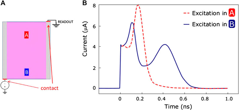
FIGURE 2. (B) The simulated current response when a charge of 2.88 fC is released in the elementary cell at two different depths, at positions A (dashed red) and B (solid blue) as shown in (A).
3. Fabrication
3.1. Experimental Setup for Laser Graphitisation
A Ti:Sapphire femtosecond laser source was used to induce a transformation of the carbon phase from diamond to a mixture of
The sensors here described were obtained with pulse width of 50 fs, repetition rate 1 kHz, wavelength of 800 nm and pulse energy of 700 nJ, as measured immediately before impinging in the diamond specimen. A schematic representation of the optical system driving the laser onto the diamond specimen is shown in Figure 3. Two beam splitters were used to arrange a photodiode, a deformable mirror and a CCD camera on the optical path. The laser is focused on the surface or in the bulk of the diamond with a 50
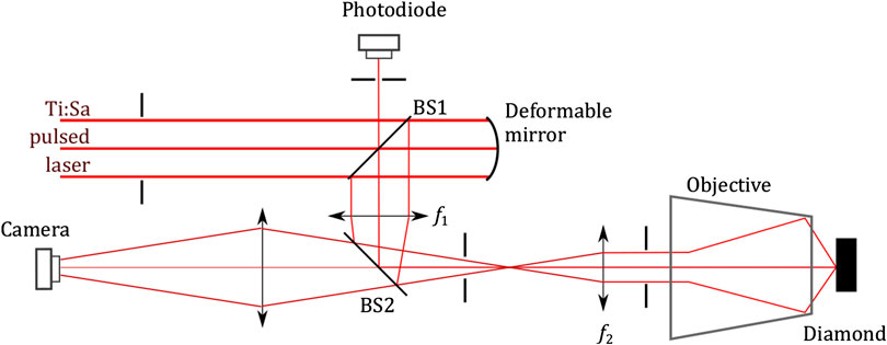
FIGURE 3. Schematic representation of the optical system. The laser beam is reflected by a deformable mirror which is imaged on the pupil of the objective. The same objective is used to acquire a microscopic image of the sample, during operations, with a CCD camera. A fast photodiode is used to monitor the beam conditions and as time reference for measurements with laser-induced charge generation.
The sample position was controlled with a three-axis displacement stage driven by computerised stepper motors with a resolution of 350 nm.
A distributed experimental control system software, interfacing the camera, the oscilloscope, the stepper motors, the deformable mirror and its temperature controller was developed and implemented on the Arduino [31] platform. The camera is connected to a computer dedicated to real-time image processing, providing measurements of the laser waist and energy profile with a rate up to 20 Hz. The energy measurement is normalised to the beam intensity as measured by the photodiode.
A client Run Controller application coordinates all the other services, providing a simplified scripting interface to define and run Python routines accessing all the described devices, while hiding the complexity of such a distributed and heterogeneous experimental setup.
3.2. Spherical Aberration: Description and Correction
The refractive index mismatch between air and diamond causes spherical aberration in the laser beam focused in the diamond bulk [32]. The effect of the spherical aberration on the focus is represented in Figure 4. The correction introduced with an adaptive optics element imaged onto the pupil of the objective by a pair of achromatic doublets in a
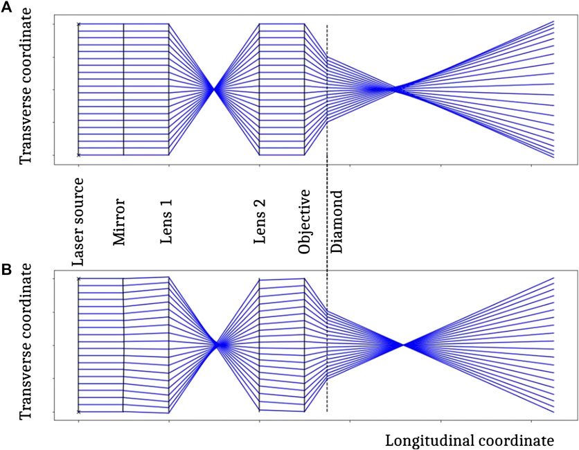
FIGURE 4. Schematic representation of the optical effect of the diamond surface on the laser beam in absence of correction (A) and with the optimal mirror deformation (B).
In paraxial approximation, the correction of the spherical aberration can be obtained, without modifying the depth in diamond z at which the maximal energy density is concentrated, by applying a phase shift [33].
to the laser beam, where ρ is the distance to the optical axis and α and β are constant parameters to be optimised. In practice, however, we found more convenient to optimise directly the voltages applied to the piezoelectric motors connected to the medium and outer rings of the deformable mirror, indicated as
The optimisation procedure is performed at several depths by maximising the quality of the laser beam spot as diffused by a opalescent coating of a wedge-shaped diamond sample. The optimisation procedure is carried out at different depths in order to infer the optimal values for
The quality of the focus is determined by processing the image
where σ is adjusted according to the magnification power of the imaging optical system. To reduce the effect of random fluctuations, the quality of the beam spot is evaluated on several consecutive acquisitions and averaged before using it to define the next mirror configuration to be explored.
The robust Nelder-Mead optimisation method [34], as implemented in the scipy libraries [35], was used to perform the optimisation procedure [36]. The voltages obtained with the optimisation procedure are displayed in Figure 5A as a function of the depth in diamond z. Even if the errors are large, especially on the optimal values for
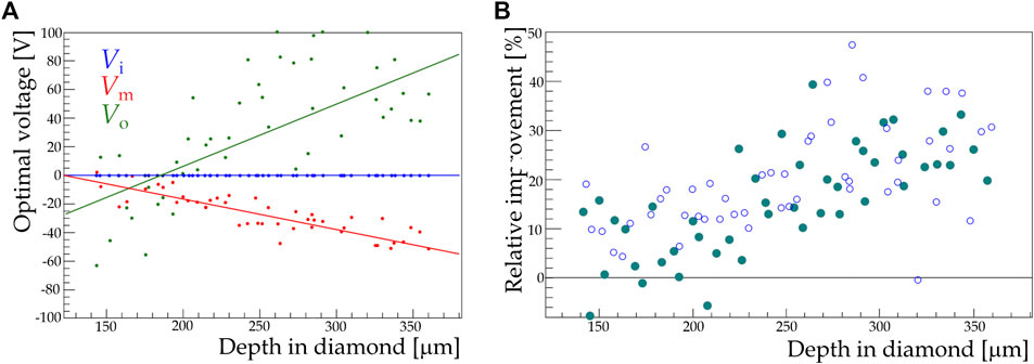
FIGURE 5. (A) The optimal values for the voltages applied to the piezoelectric motors controlling the deformable mirror as determined with an iterative optimisation procedure. A linear model describing the dependence of the optimal voltage on the depth in diamond is superimposed. (B) the relative improvement in the focus quality Q obtained from direct optimisation (empty markers) or obtaining the voltages as a function of the depth from the linear models shown in (A) (full markers).
A linear fit is performed on the optimised voltages to predict the optimal mirror configuration at a given value of z. To validate the complete procedure, we evaluated the relative improvement in the beam spot quality Q obtained with a dedicated numerical optimisation of the mirror shape and with the voltages predicted by the linear model. The results, compared in Figure 5B, are consistent with each other.
The angular coefficients of the linear models predicting the voltages were measured with this procedure several times during the year, after any maintenance intervention on the laser system or devices composing the optical system, and found stable within the uncertainties.
3.3. Electrode Engraving Procedure and Electrical Tests
The electrodes are obtained focusing the laser beam on the back of the diamond, i.e., the surface opposite to the beam entrance, and then moving the sample away along the beam direction at a speed of 20 mμ/s. The beam focus moves towards the entrance surface of the sample at a speed of 48 mμ/s, because of the higher refractive index of diamond, transforming the diamond into resistive carbon phase along the path. While the motor displaces the diamond sample, the deformable mirror is operated to correct for the spherical aberration, modifying its configuration according to the instantaneous position of the beam focus in the diamond.
The resistive columns used as electrodes for the sensor are buried in the diamond by stopping the engraving procedure at 20 mμ from the upstream surface. Columns produced to measure the resistivity of the obtained carbon phase are piercing the sample, providing two accessible ends for electrical measurements, surface tracks are engraved at the two ends with a nanosecond laser to ensure good electrical contact.
Figure 6A shows a microscopic image of a set of piercing columns engraved at 100 μm from the sample side. The resistance of the columns is measured applying different voltages to the ends of piercing columns and precisely measuring the current. Piercing columns engraved with a threshold-energy laser beam with and without the adaptive optics corrections are compared.
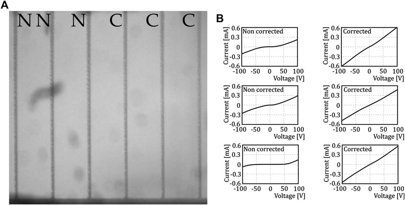
FIGURE 6. (A) A set of piercing columns with a pitch of 100 μm with (C) and without (N) correction, at threshold energy. (B) I-V curves for the piercing columns obtained with and without the optical correction.
In Figure 6B we report the measurements of the I-V curves for three columns obtained without any correction on the laser beam, and three columns obtained correcting the spherical aberration with the simultaneous displacement of sample and mirror. The improvement is evident, especially in the small-signal region. The I-V curves of columns obtained with the corrected beam are found to show a lesser deviation from ohmicity, while the uncorrected beam results into higher dynamic resistance for lower voltages.
3.4. Sensor Production and Test Electronics
Two sensors were produced with the system discussed above on sCVD samples. The first, denoted as Sensor A, was produced without any laser beam correction, with a pitch of 100 μm × 160 μm. The second, named Sensor B, was produced with a pitch of 55 μm × 55 μm to be compatible with the Timepix standard [24] and applying the correction for the spherical aberration.
Sensors A and B were prepared with
The laser beam used to produce Sensor A was adjusted to provide pulses of 1700 nJ each, while 700 nJ per pulse were used to produce Sensor B, where finer electrodes were needed to obtain a finer pitch avoiding cracks in the diamond substrate. As a consequence, the electrodes of Sensors A and B have diameters of about 30 μm and 8 μm, respectively.
An automated routine was developed to repeatedly engrave the electrodes on a single side. Slow drifts in the laser alignment, typically displacing the focus by few microns in 1 h of operations, were compensated by manually adjusting the motor position at regular intervals. Engraving
To provide test structures of different size and capacitance, surface graphitisation was induced to short circuit sets of different numbers of electrodes. For this operation, a Nd:YAG Q-switched laser source with an 8 ns pulse width, pulse energies in the range 10–60 μJ, and 1,064 nm wavelength, was used. A single sensor-wide pad was defined for Sensor A, while the electrodes of Sensor B were connected to provide several test structures: a set of strips of 5, 9, 13, 21, and 30 electrodes, and a larger comb-like pad connecting all the remaining electrodes. Strips are interleaved by elementary cells connected to the comb pad. Surface graphitisation was also used to connect the electrodes to graphitic conductive pads, sputtered with gold to allow wire bonding. Figure 7 reports an optical microscopy image of Sensor A and a schematic representation of the test structures realised on Sensor B.
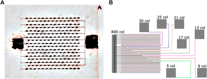
FIGURE 7. (A) An optical microscopy image of Sensor A.The electrodes are well visible as thin dark points, while the two lateral pads, on opposite diamond surfaces, are designed to allow wire bonding. (B) A schematic representation of the connections of Sensor B into several test structures, each connected to its wire-bonding pad. All the electrodes not part of a strip-shaped test structure are short-circuited and connected to the large comb-like pad on the left of the schematic.
In the configuration used for the measurements, the sensors are mounted using conductive glue on an electronic board with a hole leaving the sensor active area free in order to minimize the passive material in telescope setups. The gold-sputtered pads on the sensor are connected with 25 μm aluminium wires to the input pads of a two stage amplifier with a shaping time of 1 ns and a bandwidth of 1 GHz. A single board, designed at the University of Kansas, hosts eight such readout channels with independent amplification and shaping chains [37, 38]. A metallic cover can be installed on the board to protect the device from electromagnetic interferences, dusts and mechanical shocks that could damage the bonding wires. An aperture in the cover, aligned with the hole on the board below, reduces the material budget upstream the sensor.
4. Results
A complete study of the sensors was performed by measuring the properties of their response to two different radiation sources: a femtosecond laser generating point-like charge and diffuse charge generation provided by charged particles at minimum ionisation releasing energy along their whole path through the diamond. A comparison was made between the results obtained with two different charged particle types: the high energy electrons emitted by
In each setup, a fast and reliable time reference allowed us to measure the time resolution of sensors along with the signal-to-noise ratio.
The same readout electronics and DAQ system was used for the three measurements, to facilitate the comparison of the results, although differences in the overall experimental setup, like, e.g., cable lengths and environmental noise, may introduce unavoidable discrepancies which are difficult to correct.
4.1. Data Acquisition and Processing
Three different DAQ setups, based on LeCroy WaveRunner oscilloscopes, 610Zi, 8104 and 760Zi-a, were used to acquire the amplified signals obtained with laser, electrons and pions. All oscilloscopes were configured to operate with a 1 GHz bandwidth and 20 Gsps. The oscilloscopes were connected to the experiment control system via the LXI protocol, defining the overall configuration of the data acquisition, including the trigger strategy and a unique identifier for the data acquisition run.
The acquired data were stored on a removable memory device accessed through a fast USB or PCIe connection, in the LeCroy-standard ASCII format, which is then processed offline into a compressed binary format immediately accessible to data analysis.
4.2. Response to Laser Induced Charge Generation
The same setup described in Section 3.1 and used to induce the graphitisation of the electrodes, was used to drive an attenuated laser beam onto the polarised diamond sensor, generating charge at a well defined position
Two fast photodiodes were installed on the optical path of the Ti:Sapphire laser in order to ensure a reference time measurement substantially more precise than the expected diamond time resolution. One of the two photodiodes was positioned within the optical system used to compress the laser pulses to 50 fs, while the other is part of the graphitisation optical setup. The former is found to be more stable during long data taking periods and it is therefore chosen as reference. The latter is sensitive to the slow oscillations of the laser beam and it is therefore only used to set an upper limit on the time resolution of the reference.
The jitter of the measured time difference of the two photodiode signals was found to be less than 20 ps which defines an upper limit on the single photodiode time resolution.
For each measurement, the laser beam was focused in the bulk of the diamond sensor in 2500 randomly chosen positions scanning the volume of four elementary cells. The signals obtained from Sensor A and from the strip-shaped pad of 30 elementary cells of Sensor B are acquired for 5 s for each of the chosen positions. Even if the laser is operated at a pulse frequency of 1 kHz, because of the oscilloscope dead time only about 200 waveforms are acquired in this interval. Averaging the waveforms acquired for each laser spot position, the noise contribution is reduced and the dependence of the sensor response on the position of the laser spot can be precisely analysed.
Figure 8 reports the amplitude of the averaged signals as a function of the position of the laser excitation for both Sensor A and Sensor B. With a careful choice of the colour code, different regions of the elementary cell are visualised. On Sensor A, we observe large signals for excitations close to the electrodes not connected to the readout electronics. In these regions, the higher electric field causes the signal to be much faster and therefore a larger fraction of the generated charge is integrated by the readout electronics. In the neighbourhood of these electrodes the signal amplitude exceeds the signal amplitude collected in the midpoint between pairs of oppositely polarised electrodes by one order of magnitude. The lack of signal in the uppermost region of the readout electrodes, connected to the electronics, is interpreted as a shadow effect of the superficial graphite connection and of the electrode itself. Thinner columns and smaller elementary cells are beneficial to the uniformity of the response, as shown by the measurement on Sensor B. The position of the electrodes can be barely identified from a mild increase in the amplitude and the signal is observed up to few microns from the electrode. On the other hand, the larger resistance of the electrodes results into an evident dependence of the response on the excitation depth, with the average signal amplitude on the forward surface twice as large as on the backward surface.
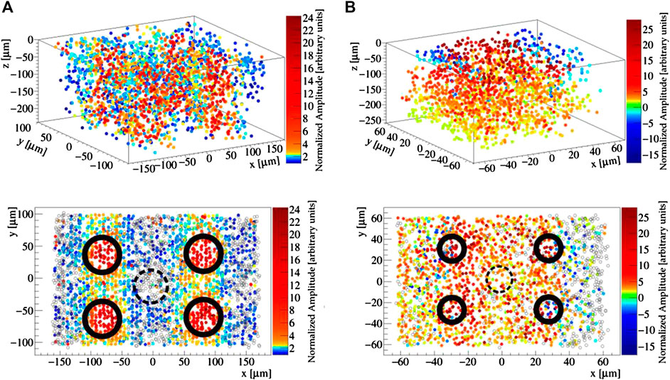
FIGURE 8. Graphical representation of the dependence of the signal amplitude on the point of excitation of Sensor A (A) and Sensor B (B) with Ti:Sapphire laser pulses. The three-dimensional scans depicted on the top, are projected onto the transverse plane
The strip-shaped test structure of Sensor B allows one to study effects of cross-talk between neighbouring elementary cells. First of all, we observe a negative signal when exciting the sensor close to the surface, immediately outside of the active area. This effect is well known for silicon detectors and it is due to a capacitive coupling between adjacent elementary cells. This effect is beneficial to the interpretation of Figure 8 because it clearly identifies the borders of the active area of the read elementary cell, as the sharp transition from large positive to large negative signals. Unexpectedly, however, while the position at which we observe negative response follows the symmetry of the elementary cell, we observe different response of the test structure to excitations to the left and to the right adjacent cells. When generating charge in Sensor B at x larger than the cell boundary (
The observed asymmetric cross-talk effect is not fully understood and may depend on local defects in the diamond sample. We notice that, as a consequence of the cross-talk, the description of the averaged response of the test structures to impinging ionising particles discussed in the next sections is subject to an unavoidable background from cross-talk.
Each waveform acquired for each position is processed by a digital Constant Fraction Discriminator (CFD) algorithm to obtain the delay of the signal with respect to the fast trigger signal received from the photodiode. To enhance robustness against the electronic noise, the CFD algorithm scans the acquired waveforms to compute and subtract the baseline in order to identify the global maximum of the two samples describing the transition of the waveform through a threshold at 35% of the maximum signal amplitude, and finally refines the computation of the time marker with a linear fit of the leading edge.
An averaged delay is computed out of the set of about 200 measurements obtained for each scanned position. Since the residual contribution of the electronic noise on the average delay is marginal, the measurement is sensitive enough to allow obtaining the distribution of the delays as a function of the position of the laser spot. Figure 9 shows the distributions of the averaged delays as obtained for Sensor A and the strip-shaped test structure of Sensor B.
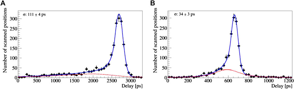
FIGURE 9. Distribution of the delay between the time reference defined by the photodiode and the time marker on Sensor A (A) and Sensor B (B). The superimposed fit, used to determine the resolution of the main peak, describes the dataset as the combination of a signal component modelled with a Crystal Ball function, and a background component modelled with the empirical function defined in Eq. 3.
Both distributions show an evident non-Gaussian tail at left of the main peak, populated by the samples obtained exciting the sensor in the regions with the highest field, close to the electrodes. In order to quantify the spread of the distribution, we model the dataset as the combination of a signal component modelled with a Gaussian with an asymmetric tail, named Crystal Ball function [39] and an empirical parametrisation of a non-peaking contribution defined as
where
As expected, the width of the main peak is smaller for Sensor B than it is for Sensor A, which indicates that the more homogeneous electric field obtained with fine-pitched thin electrodes is important to control the contribution to the sensor resolution related to the charge collection mechanism.
Throughout the paper, we define the resolution as the standard deviation of the Gaussian core of the Crystal Ball modelling the signal peak.
The obtained resolutions are
As expected, resolution is smaller for Sensor B than for Sensor A, this indicates that the more homogeneous electric field obtained with fine-pitched thin electrodes is important to control the contribution to the sensor resolution due to the spread of the collection time.
We notice also that, due to the signal dependence on the generation position, the resolution obtained with the laser excitation mechanism tends to overestimate the contribution from inhomogeneities of the sensor response to the overall sensor resolution with respect to the case of ionising particles. Indeed, with the laser the charge is generated in the single position where the beam is focused on, while for the particles the charge is generated along the whole thickness of the sensor, averaging therefore over different depths and, to a lesser extent, distances from the readout electrode.
4.3. Response to Electrons From a
The response of the sensor to minimum-ionising particles has been measured with electrons from a 270 MBq 90Sr β source. In the decay chain 90Sr→90Y
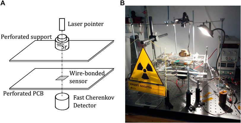
FIGURE 10. Schematic drawing (A) and picture (B) of the experimental setup used to study the sensor response to electrons from 90Sr.
The acquisition of the sensor signal waveform is triggered by the coincidence of a pulse from the MCP-PMT and a signal from the sensor in a time window of 10 ns. This requirement is necessary to select electrons traversing the sensor, because of the much larger active area of the Cherenkov detector with respect to the test structures in the diamond, which is illuminated by the non collimated 90Sr source.
For each test structure, the sensor trigger threshold is optimised by reducing the noise counting rate to a few percent of the maximum rate allowed by the oscilloscope dead time.
The test structures probed with the β source are Sensor A, the strip-shaped pads of Sensor B composed of 5, 9, 21, and 30 elementary cells and the large comb-like pad obtained short-circuiting the readout electrodes of 822 elementary cells.
For each test structure we acquire data in 6–8 h long runs, corresponding, on average, to
The analysis of the acquired data and of data from the 270 MeV/c pion test beam are discussed jointly in the next Section.
4.4. Response to Minimum-Ionizing Pions in a Beam Test
While the study of the sensor response with β rays allows one to acquire large datasets under a large variety of operational conditions, the electrons produced in the decay are subject to significant multiple scattering that can in principle bias the response of the detector. The low energy of the probe particles requires special care in reducing the inactive material traversed by particles in the experimental setup. A complementary study of the response of the detector was therefore performed with a beam of pions with momentum
The experimental setup, shown in Figure 11, consists of two Cherenkov detectors with quartz radiators and MCP readout placed downstream of the test structures. To enhance the effectiveness of the study, several test structures of diamond detectors were studied simultaneously. The mechanical structure was designed to allocate up to three 10 cm wide PCBs upstream of the Cherenkov detectors. To protect the MCP from ambient light, the experimental setup was enclosed in a black box, with sets of connectors to provide power to the electronics, polarisation voltages to the sensors and to connect the output of the amplifiers to the oscilloscopes used for the data acquisition. To reduce the material upstream the senors under test, the beam enters the black box through a 2 cm wide circular aperture closed by a black plastic film to shield the ambient light.
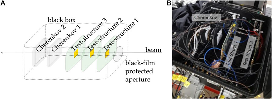
FIGURE 11. Experimental setup adopted to study the response of the diamond detector to minimum-ionizing pions at PSI. The setup is sketched in (A) and represented in photo in (B).
To mitigate the risk of radiation damage, the oscilloscopes were placed behind a concrete wall and connected to the readout boards with 10 m long low-loss cables at the cost of a slight worsening of the time resolution due to the attenuation of the signal fast components. This effect was studied in detail and found to be negligible in the determination of the time resolution of diamond sensors.
As in the case of electrons from 90Sr, the Cherenkov radiation threshold is used to select relativistic particles, at minimum ionisation. The πM1 beam line is composed by equal momentum particles, predominantly pions, with smaller components of protons, muons and positrons. In particular the proton component is populated by primary protons that lost their energy in the pion production target [42]. These low energy protons do not behave as minimum-ionising particles and tend to release large energy deposits in the sensors, biasing the measurements. These protons are filtered out by inserting on the beam path a 4 mm thick plastic layer. The residual protons passing the absorbers are too slow to produce Cherenkov radiation and are therefore easily rejected by the triggering system. To study the composition of the beam downstream of the absorber, the signal driving the electrical field of the cyclotron accelerator is acquired together with the two MCP-PMT and diamond signals. The time difference
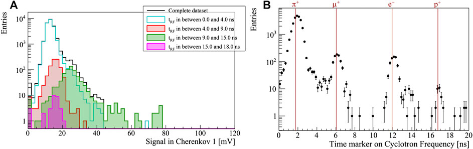
FIGURE 12. (A) The distribution of the signal from the upstream Cherenkov detectors in four intervals of the relative radio frequency time
As expected, the dominant contribution is from pions, with a few percent level contamination of muons and positrons, both minimum-ionizing particles, and a sub-permille contribution consistent with the proton mass hypothesis. The latter is interpreted as a background of δ-rays produced in interactions of protons with the black box entrance window. Such lower-energy electrons are still minimum-ionisation particles, with sufficient velocity to produce Cherenkov light.
To take into account potential small systematic differences among the readout channels connected to the different sensors and electrode layouts that may induce unwanted biases in the results, data have been acquired in two different readout configurations: the first with exactly the same setup as for the test with 90Sr source; the second with readout channels swapped between different test structures.
4.5. Data Analysis
The data collected with electrons and pions beams described above are analysed to measure and compare the time resolution of the two sensors.
The most evident feature of the acquired waveforms is the low signal-to-noise ratio. Figure 13 reports sixteen random examples of waveforms acquired during the beam test with minimum-ionising pions and the setup described above. Significant signal shape variations are clearly visible notwithstanding the large noise, that introduce undesired time-walk contributions to the timing uncertainty. On the basis of the laser-based studies on the response uniformity within the same elementary cell, such variability can be explained with inhomogeneities of the electric field only partially. Other contributions may be for example the different charge generation mechanism, fabrication differences between electrodes composing the same test structure, and even cross-talk effects.
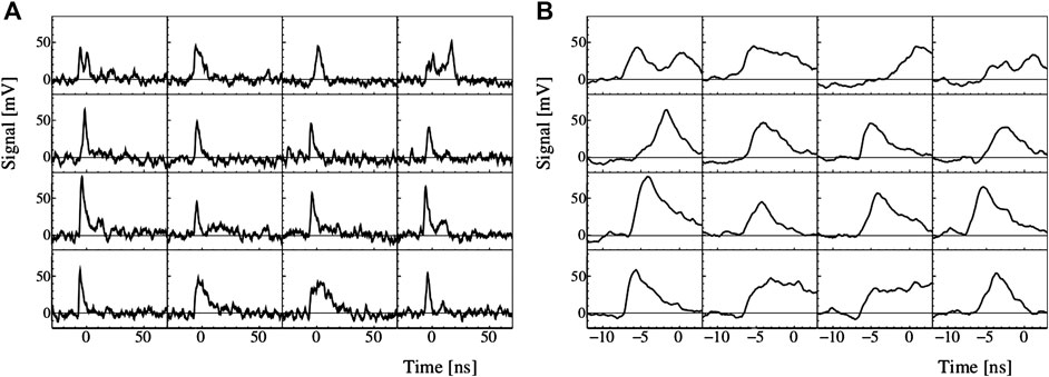
FIGURE 13. Randomly selected signals obtained from Sensor B strip composed of 30 elementary cells, with an amplitude larger than 40 mV. (A) The full time window is shown, while a zoom on the leading edge of the same events is presented (B).
Two preliminary studies performed on Sensor B prior to any waveform analysis are presented in Figure 14. In the first, the polarisation voltage of the sensor has been varied from −100 to +125 V while acquiring at fixed trigger threshold. Outside this voltage range the baseline of the acquired waveforms presents slow and wide oscillations that we interpret as early symptoms of breakdown. A slight asymmetry in the trigger rate between the positive and negative polarisation voltages, favours the former configuration. This might be related to the an asymmetry of the carrier mobility or to defects introducing junction or tip effects. We notice however that other elements of the acquisition chain in addition to the diamond sensor may introduce asymmetries between positive and negative signals. This conclusion is therefore limited to the particular combination of sensors, electronics and oscilloscope used in the analysis. The maximum applicable voltage seems sufficient to reach saturation for negative voltages while a higher voltage may result in higher trigger rate for positive voltages. In both cases, the saturation voltage is close to the breakdown voltage. Considering the large electric field in proximity of the tip at the end of the electrodes, it is reasonable to conclude that the geometrical regions where the charge generation and the breakdown take place are different. The distance between the conductive electrodes and the surface of the diamond limits the polarisation voltage to values that are at most barely sufficient to reach the saturation velocity of the carriers in the whole volume.
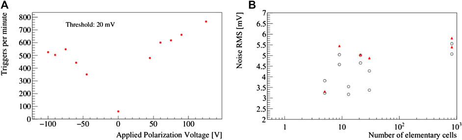
FIGURE 14. (A) The study of the trigger rate as a function of the polarisation voltage. (B) RMS noise as a function of the number of short-circuited elementary cells in several different measurements. In particular, measurements performed during the beam test are represented as red markers, while measurements in the setup with the 90Sr source represented as black empty markers.
A second preliminary study concerns the electronic noise. Because of their large band-gap, the dark current and therefore the shot contribution to the electronic noise is negligible in diamond sensors. The large resistance of the electrodes results into a large contribution to the Johnson or thermal noise which is supposed to scale as the square root of the number of elementary cells merged in a test structure. Experimentally, however, no significant correlation between the number of short-circuited electrodes and the measured noise is observed. The tiny capacitance of the elementary cells, estimated of the order of 35 fF per cell is so small compared to the input capacitance of the readout electronics that combining together more than 800 elementary cells results into a barely measurable increase of the noise RMS voltage. The noise RMS voltage measured for Sensor A is perfectly consistent with the values reported in Figure 14 obtained for the various structures of Sensor B. The noise spectrum was analysed and found consistent among the various experimental setups, with negligible contribution from pickup. Dedicated pixel electronics with precise timing capabilities is being developed and will allow for a drastical reduction of the input capacitance of the front-end and hence the noise [43].
Because of the significant cross-talk observed when exciting the diamond sensor with a laser beam as discussed in Section 4.2, some of the weakest signal events may be interpreted as due to particles traversing the device outside of the active region. Unfortunately, without a precise information on the position of the particle entering the detector it is impossible to measure the detection efficiency or to identify the amplitude distribution of the particles entering the active area of the detector. Since the electrons produced in the 90Sr decay chain have insufficient energy to release charge in several planes of a tracking telescope, such a measurement is postponed to a future beam test.
The distribution of the delays between the diamond and reference signals for the 30-cell test structure of Sensor B as obtained with β rays is shown as an example in Figure 15B. The result of a fit to the distributions of delays is shown superimposed to the data. The data are fitted with the sum of a Crystal Ball function modelling the peak and the empirical function in Eq. 3 to describe the background of random coincidences.
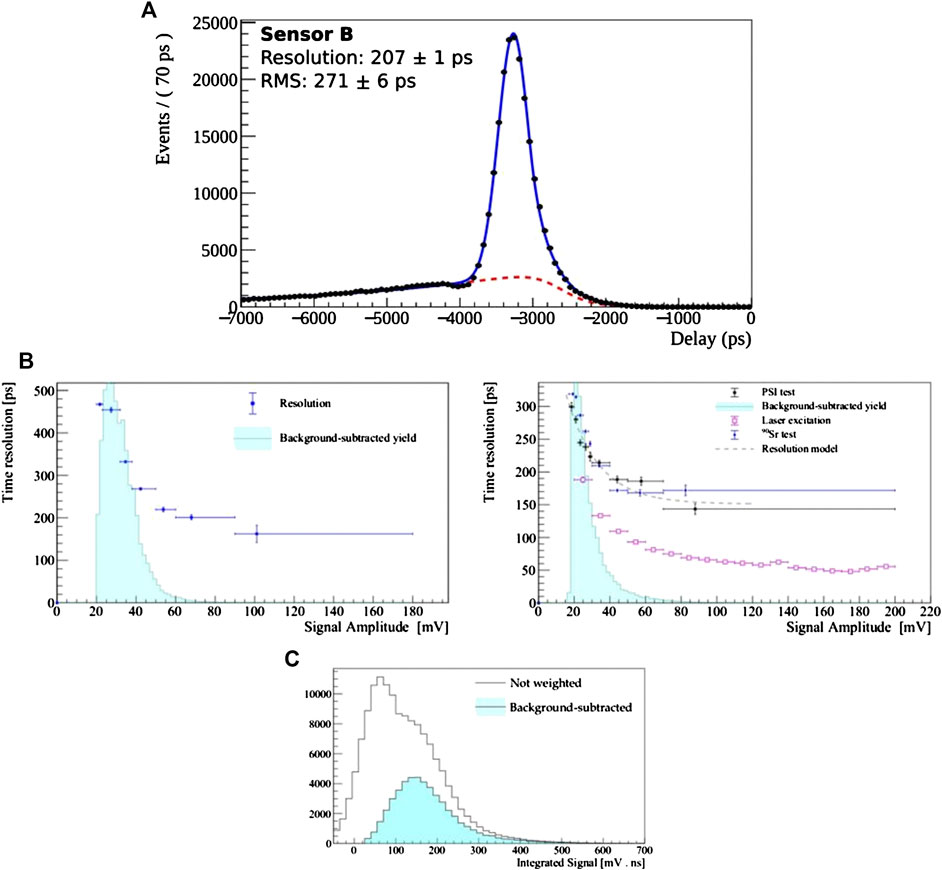
FIGURE 15. (A) Fit of the delay distribution with a Crystal Ball function superimposed to non-peaking background. (B) Study of the resolution of the sensors A and B, respectively, in bins of the signal amplitude. The histogram of the signal amplitude obtained with the s
The same fitting procedure has been repeated in bins of signal amplitude to study the dependence of the time resolution on the signal shape. The dependence of the resolution as a function of the amplitude is presented in Figure 15B, for both Sensor A and B as obtained from 90Sr electron data. For sensor B, the same dependencies obtained with laser and minimum-ionising pions are also shown on Figure 15B; only the results from the 30-cells strip are shown, the results from the other test structures being substantially equivalent. In order to add context to the dependence of the resolution on the amplitude, the distribution of the latter, as obtained with the β source setup, is represented on the background of the two plots in Figure 15B. Such a distribution is obtained by applying the s
As expected, the beam test data confirm the results obtained with the β source, while the timing of laser excitations is determined with significantly better time resolution because of the different distribution of the generated charge within the diamond. The strong dependence of the resolution on the signal amplitude highlights once more the dominant effect of the electronic noise in the determination of the uncertainty on the timing measurement.
From the comparison of the resolutions obtained with the two sensors (see Figure 15B), a significant improvement is evident when moving from Sensor A to Sensor B. The improvement is confirmed also using different time resolution estimators, including the signal peak FWHM, and the variance of the peak fitted with a Crystal Ball function. The time resolution improvement from Sensor A to sensor B varies between 20 and 40% depending on the estimation used.
Different algorithms to assign the time marker to the acquired waveforms have been compared. The performance of each algorithm has been evaluated on the basis of the number of signal rising edges correctly identified and on the resulting time resolution. Substantial effort has been spent to find the optimal balance between high detection efficiency and best time resolution. Although details of this study are outside the scope of this paper, a clear outcome is that corrections for the signal leading edge slew rate are needed to significantly improve the time resolution. These corrections seem to confirm the effects of electric field inhomogeneities observed with the laser tests. Its spread seems too large to be due uniquely to noise fluctuations and may result from inhomogeneous electrical field within the sensor, as already pointed out with laser based studies.
To provide another benchmark time resolution estimation for future reference, in addition to the measurement with the digital CFD used throughout this paper, an analog Constant Fraction Discriminator (aCFD) algorithm has been implemented. In the aCFD, a delayed attenuated copy of the signal is subtracted from the signal itself giving as an optimal time marker the zero-crossing time of the resulting bipolar signal. The aCFD provides a complete cancellation of time slewing effects but is sensitive to noise fluctuations that distort the signal, giving rise to false triggers. As a consequence, aCFD offers a better time resolution than the baseline CFD but it shows a decreased tagging efficiency. Indeed using the aCFD (simple CFD) algorithm we obtained a time resolution of 207 ± 1 ps (263 ± 1 ps) from a sample of
5. Conclusion and Future Prospects
This paper reports on the first detailed study of the time resolution of 3D pixel diamond sensors. The investigation was carried out by comparing the response of two different sensors to different excitations: minimum-ionising pions, electrons and laser pulses. The main result emerging from this study is the fact that thinner and finer pitch columnar graphite electrodes improve significantly the time resolution, while, at the same time, matching better the requirements in terms of space resolution. Although the timing performances of the diamond devices presented in this work are not yet competitive with those of 3D silicon sensors, this study has allowed identifying the key elements to proceed towards a further optimisation of these devices, discussed in this Section.
5.1. Front-End Electronics
It is evident that the dominant contribution to the time resolution is the electronic noise at the input of the amplifier. The experimental setup with long bonding wires and discrete electronic components seems to introduce dominant noise contributions to the pixel noise, as made evident by the mild dependence of the noise level on the number of short-circuited elementary cells. The development of microelectronics with high-resolution timing capabilities is part of the
5.2. Column Resistivity
The high resistivity of the graphitised columns increases the time constant of the pixel and slows down the extraction of the signal from the bulk of diamond. The progress obtained with an improved focusing of the laser, using adaptive optics to correct the spherical aberration of the wavefront due to the air-diamond interface is evident. However the setup based on a deformable mirror adapted with an iterative procedure based on the laser spot image leads to instabilities that negatively affects the quality of the electrodes and ultimately the sensor time resolution. In particular, we found that small variations of the room temperature result into significant modifications of the mirror curvature, and therefore of the laser divergence. The nanofabrication optical system is being upgraded to replace the deformable mirror with a Liquid-Crystal-on-Silicon Spatial Light Modulator [45], which allows for a much more precise implementation of the theoretically computed phase-shifts necessary to the correct for spherical aberration [33].
5.3. Column Geometry
The maximal polarisation voltage was found to be roughly the same on Sensor A and Sensor B, and in general is observed to be roughly independent of the sensor pitch. While unexpected, this result may be understood once the 3D maps obtained with laser excitation are carefully considered. The highest field region is close to the tip of the columnar electrodes: the probability of discharge in this region is clearly independent of the pixel pitch being only affected by the distance between the tip of the electrode and the diamond surface. In other words, the analysed sensors are operated at a voltage which is probably too low to reach the saturation velocity of the carriers within the whole volume, leading to a dependence of signal shape on the position where the charge is generated, worsening the time resolution by effect of an increased spread in the collection time. An optimisation of the geometry close to the end of the electrodes will be carried out and implemented in the next batch of sensors. Improved time resolution obtained in 3D Silicon devices with trench-shaped electrodes [4] suggests to replicate such geometry in diamond sensors, by suitably shaping the nanofabrication laser beam to obtain electrodes with lower resistance and pixels with a more uniform electrical field. Similarly, a further reduction of the column pitch should also be investigated.
The identification and the solution of the above issues largely defines the next steps of our development of 3D pixel diamond sensors. The results discussed in this paper are already extremely encouraging and represent a further step towards the application of 3D diamond sensors to tracking detectors with timing capabilities in future experiments at colliders in extreme radiation conditions.
Data Availability Statement
The raw data supporting the conclusions of this article will be made available by the authors, without undue reservation.
Author Contributions
LA, MB, CC, SL, SM and SS designed and fabricated the sensors; RC, SL, NM, AM, DP and MV developed different parts of the simulations; LA, AC, SL, CL, GP, SS and MV characterised the electrodes and the sensors with table-top measurements; LA, AB, AC, MG, AdL, AL (10th author), AL (11th author), CL, NM, RM, SV and MV made the beam test at PSI possible and contributed to the data analysis.
Funding
The research described in this document was funded by INFN as part of the TimeSPOT initiative.
Conflict of Interest
The authors declare that the research was conducted in the absence of any commercial or financial relationships that could be construed as a potential conflict of interest.
Acknowledgments
We acknowledge Patrick Salter for his valuable help with the setup of the aberration-correcting optics, Harris Kagan for enlightening discussion on the front-end electronics, Sara Nocentini for taking care of the surface metallisation of the diamond specimens, Mirko Brianzi and Silvan Stamm for the wire-bonding procedure, and Angela Papa for the support during the activities at PSI.
Footnote
References
1.The ATLAS and CMS Collaborations. Report on the physics at the HL-LHC and perspectives for the HE-LHC. arXiv:1902.10229 (2019).
2.LHCb collaboration. Physics case for an LHCb Upgrade II-opportunities in flavour physics, and beyond, in the HL-LHC era. arXiv.1808.08865 (2018).
3. Sola, V, Arcidiacono, R, Cartiglia, N, Ferrero, M, Mandurrino, M, and Staiano, A. Fast timing detectors towards a 4-dimensional tracking. In: PoS (2019) ICHEP2018:594. doi:10.22323/1.340.0594
4. Anderlini, L, Aresti, M, Bizzeti, A, Boscardin, M, Cardini, A, Betta, GFD, et al. Intrinsic time resolution of 3D-trench silicon pixels for charged particle detection. arXiv:2004.10881 (2020). Accepted by JINST.
5. Pellegrini, G, Fernández-Martínez, P, Baselga, M, Fleta, C, Flores, D, Greco, V, et al. Technology developments and first measurements of low gain avalanche detectors (LGAD) for high energy physics applications. Nucl Instrum Methods Phys Res Sect A Accel Spectrom Detect Assoc Equip (2014). 765:12–6. doi:10.1016/j.nima.2014.06.008
6. Garcia-Sciveres, M, and Wermes, N. A review of advances in pixel detectors for experiments with high rate and radiation. Rep Prog Phys (2018). 81:066101. doi:10.1088/1361-6633/aab064
7. Cartiglia, N, Staiano, A, Sola, V, Arcidiacono, R, Cirio, A, Cenna, F, et al. Beam test results of a 16 ps timing system based on ultra-fast silicon detectors. Nucl Instrum Methods (2017). A850:83–8. doi:10.1016/j.nima.2017.01.021.
8. Aleksa, M, Blomer, J, Cure, B, Campbell, M, D’Ambrosio, C, Dannheim, D, et al. Strategic R&D programme on technologies for future experiments (2018). CERN. Technical Report CERN-OPEN-2018-006.
9. Kramberger, G, Carulla, M, Cavallaro, E, Cindro, V, Flores, D, Galloway, Z, et al. Radiation hardness of thin low gain avalanche detectors. Nucl Instrum Methods Phys Res Sect A Accel Spectrom Detect Assoc Equip (2018). 891:68–77. doi:10.1016/j.nima.2018.02.018
10. Kramberger, G, Baselga, M, Cindro, V, Fernandez-Martinez, P, Flores, D, Galloway, Z, et al. Radiation effects in low gain avalanche detectors after hadron irradiations. J Inst Met (2015). 10:P07006. doi:10.1088/1748-0221/10/07/P07006
11. Lange, J, Giannini, G, Grinstein, S, Manna, M, Pellegrini, G, Quirion, D, et al. Radiation hardness of small-pitch 3D pixel sensors up to a fluence of 3×10¹⁶ neq/cm2
12. Kramberger, G, Cindro, V, Flores, D, Hidalgo, S, Hiti, B, Manna, M, et al. Timing performance of small cell 3D silicon detectors. Nucl Instrum Methods Phys Res Sect A Accel Spectrom Detect Assoc Equip (2019). 934:26–32. doi:10.1016/j.nima.2019.04.088
13. Bossini, E, and Minafra, N. Diamond detectors for timing measurements in high energy physics. Front Physiol (2020). 8:248. doi:10.3389/fphy.2020.00248
14. Bauer, C, Baumann, I, Colledani, C, Conway, J, Delpierre, P, Djama, F, et al. Radiation hardness studies of CVD diamond detectors. Nucl Instrum Methods Phys Res Sect A Accel Spectrom Detect Assoc Equip (1995). 367:207–11. doi:10.1016/0168-9002(95)00545-5
15. Bachmair, F, Bäni, L, Bergonzo, P, Caylar, B, Forcolin, G, Haughton, I, et al. A 3D diamond detector for particle tracking. Nucl Instrum Methods (2015). A786:97–104 [Erratum: Nucl. Instrum. Meth.A797,331(2015)]. doi:10.1016/j.nima.2015.03.033.
16. Böni, L, Alexopoulos, A, Artuso, M, Bachmair, F, Bartosik, M, Beck, H, et al. A study of the radiation tolerance of poly-crystalline and single-crystalline CVD diamond to 800 MeV and 24 GeV protons. J Phys D (2019). 52:465103. doi:10.1088/1361-6463/ab37c6
17. Lagomarsino, S, Bellini, M, Corsi, C, Cindro, V, Kanxheri, K, Morozzi, A, et al. Radiation hardness of three-dimensional polycrystalline diamond detectors. Appl Phys Lett (2015). 106:193509. doi:10.1063/1.4921116
18. Adam, W, Bauer, C, Berdermann, E, Bogani, F, Borchi, E, Bruzzi, M, et al. Development of diamond tracking detectors for high luminosity experiments at the LHC (1996). CERN-LHCC-97-003.
19. Lagomarsino, S, Bellini, M, Corsi, C, Gorelli, F, Parrini, G, Santoro, M, et al. Three-dimensional diamond detectors: charge collection efficiency of graphitic electrodes. Appl Phys Lett (2013). 103:233507. doi:10.1063/1.4839555
20. Reichmann, M, Alexopoulos, A, Artuso, M, Bachmair, F, Böni, L, Bartosik, M, et al. New test beam results of 3d and pad detectors constructed with poly-crystalline cvd diamond. Nucl Instrum Methods Phys Res Sect A Accel Spectrom Detect Assoc Equip (2019). 958:162675. doi:10.1016/j.nima.2019.162675
21. Lagomarsino, S, Bellini, M, Corsi, C, Fanetti, S, Gorelli, F, Liontos, I, et al. Electrical and raman-imaging characterization of laser-made electrodes for 3d diamond detectors. Diam Relat Mater (2014). 43:23. doi:10.1016/j.diamond.2014.01.002
22. Gracio, JJ, Fan, QH, and Madaleno, JC. Diamond growth by chemical vapour deposition. J Phys D Appl Phys (2010). 43:374017. doi:10.1088/0022-3727/43/37/374017
23. Schwander, M, and Partes, K. A review of diamond synthesis by CVD processes. Diam Relat Mater (2011). 20:1287–301. doi:10.1016/j.diamond.2011.08.005
24. Llopart, X, Ballabriga, R, Campbell, M, Tlustos, L, and Wong, W. Erratum to "Timepix, a 65 k programmable pixel readout chip for arrival time, energy and/or photon counting measurements" [Nucl. Instr. and Meth. A. 581 (2007) 485-494]. Nucl Instrum Methods Phys Res Sect A Accel Spectrom Detect Assoc Equip (2008). 585:106–8. [Erratum: Nucl. Instrum. Meth.A585,106(2008)]. doi:10.1016/j.nima.2007.11.003.
25. Shockley, W. Currents to conductors induced by a moving point charge. J Appl Phys (1938). 9:635–6. doi:10.1063/1.1710367
26. Morozzi, A, Passeri, D, Kanxheri, K, Servoli, L, Lagomarsino, S, and Sciortino, S. Polycrystalline CVD diamond device level modeling for particle detection applications. J Inst Met (2016). 11:C12043. doi:10.1088/1748-0221/11/12/c12043
27. Morozzi, A, Sciortino, S, Anderlini, L, Servoli, L, Kanxheri, K, Lagomarsino, S, et al. 3D diamond tracking detectors: numerical analysis for timing applications with TCAD tools. J Inst Met (2020). 15:C01048. doi:10.1088/1748-0221/15/01/c01048
28. Field, JE. The properties of natural and synthetic diamond. In: Crystal Research and Technology. Vol. 28. London, UK: Academic Press (1992). p. 602. doi:10.1002/crat.2170280504
29. Lagomarsino, S, Bellini, M, Corsi, C, Fanetti, S, Gorelli, F, Liontos, I, et al. Electrical and raman-imaging characterization of laser-made electrodes for 3d diamond detectors. Diam Relat Mater (2014). 43:23–8. doi:10.1016/j.diamond.2014.01.002
30. Lagomarsino, S, Bellini, M, Brianzi, M, Carzino, R, Cindro, V, Corsi, C, et al. Polycrystalline diamond detectors with three-dimensional electrodes. Nucl Instrum Methods Phys Res Sect A Accel Spectrom Detect Assoc Equip (2015). 796:42–6. doi:10.1016/j.nima.2015.03.041. Proceedings of the 10th International Conference on Radiation Effects on Semiconductor Materials Detectors and Devices.
31. Mellis, D, Banzi, M, Cuartielles, D, and Igoe, T. Arduino: an open electronic prototyping platform. Proc. Chi (2007). 2007:1–11.
32. Simmonds, RD, Salter, PS, Jesacher, A, and Booth, MJ. Three dimensional laser microfabrication in diamond using a dual adaptive optics system. Optic Express (2011). 19:24122–8. doi:10.1364/OE.19.024122
33. Salter, PS, Baum, M, Alexeev, I, Schmidt, M, and Booth, MJ. Exploring the depth range for three-dimensional laser machining with aberration correction. Optic Express (2014). 22:17644–56. doi:10.1364/OE.22.017644
34. Nelder, JA, and Mead, R. A simplex method for function minimization. Comput J (1965). 7:308–13. doi:10.1093/comjnl/7.4.308
35. Virtanen, P, Gommers, R, Gommers, R, Oliphant, TE, Haberland, M, Reddy, T, et al. SciPy 1.0: fundamental algorithms for scientific computing in python. Nat Methods (2020). 17:261–72. doi:10.1038/s41592-019-0686-2
36. Gao, F, and Han, L. Implementing the Nelder-Mead simplex algorithm with adaptive parameters. Comput Optim Appl (2012). 51:259–77. doi:10.1007/s10589-010-9329-3
37. Minafra, N, Al Ghoul, H, Arcidiacono, R, Cartiglia, N, Forthomme, L, Mulargia, R, et al. Test of ultra fast silicon detectors for picosecond time measurements with a new multipurpose read-out board. Nucl Instrum Methods Phys Res Sect A Accel Spectrom Detect Assoc Equip (2017). 867:88–92. doi:10.1016/j.nima.2017.04.032
38. Minafra, N. Development of a timing detector for the TOTEM experiment at the LHC. [PhD thesis]. Bari (Italy): INFN (2016). CERN-THESIS-2016-016.
39. Skwarnicki, T. A study of the radiative cascade transitions between the Upsilon-prime and Upsilon resonances. [PhD thesis]. Krakow (Poland): Institute of Nuclear Physics (1986). DESY-F31-86-02.
40. Agostinelli, S, Allison, J, Amako, K, Apostolakis, J, Araujo, H, Arce, P, et al. Geant4—a simulation toolkit. Nucl Instrum Methods Phys Res Sect A Accel Spectrom Detect Assoc Equip (2003). 506:250–303. doi:10.1016/S0168-9002(03)01368-8
42. Gilman, R, Downie, EJ, Ron, G, Strauch, S, Afanasev, A, Akmal, A, et al. Technical design report for the paul scherrer institute experiment r-12-01.1: studying the proton radius puzzle with
43. Piccolo, L. A timing pixel front-end design for hep experiments in 28 nm cmos technology. In: 2019 15th Conference on Ph.D research in microelectronics and electronics (PRIME); 2019 July 15–18; Lausanne, Switzerland. IEEE (2019). p. 205–8. Available from: https://ieeexplore.ieee.org/Xplore/home.jsp.
44. Pivk, M, and Le Diberder, FR.
Keywords: tracking, diamond, 3D, pixel, sensors, nanofabrication
Citation: Anderlini L, Bellini M, Bizzeti A, Cardini A, Ciaranfi R, Corsi C, Garau M, Lai A, Lagomarsino S, Lampis A, Loi A, Lucarelli C, Mariani S, Minafra N, Morozzi A, Mulargia R, Passaleva G, Passeri D, Sciortino S, Vecchi S and Veltri M (2020) Fabrication and Characterisation of 3D Diamond Pixel Detectors With Timing Capabilities. Front. Phys. 8:589844. doi: 10.3389/fphy.2020.589844
Received: 31 July 2020; Accepted: 22 September 2020;
Published: 04 November 2020.
Edited by:
Paul Sellin, University of Surrey, United KingdomReviewed by:
Enrico Junior Schioppa, University of Salento, ItalyDavid Pennicard, Helmholtz Association of German Research Centers (HZ), Germany
Copyright © 2020 Anderlini, Bellini, Bizzeti, Cardini, Ciaranfi, Corsi, Garau, Lai, Lagomarsino, Lampis, Loi, Lucarelli, Mariani, Minafra, Morozzi, Mulargia, Passaleva, Passeri, Sciortino, Vecchi and Veltri. This is an open-access article distributed under the terms of the Creative Commons Attribution License (CC BY). The use, distribution or reproduction in other forums is permitted, provided the original author(s) and the copyright owner(s) are credited and that the original publication in this journal is cited, in accordance with accepted academic practice. No use, distribution or reproduction is permitted which does not comply with these terms.
*Correspondence: Lucio Anderlini, Lucio.Anderlini@fi.infn.it