

Abstract
A single electron pump was incorporated with a quantum Hall resistance and a Josephson voltage for the current evaluation in the framework of Ohm's law. The pump current of about 60 pA level was amplified by a stable amplifier with a gain of 103 to induce a Hall voltage of about 60 mV level across a 1 MΩ Hall resistance array, which was compared with the Josephson voltage. The gain of the current amplifier was calibrated with a cryogenic current comparator bridge. For two different drive frequencies and repeated thermal cycles, the comparisons demonstrated that the pump current averaged over the first plateau was equal to ef within the combined uncertainty level of 0.3 × 10⁻⁶ (k = 1).
Export citation and abstract BibTeX RIS

Original content from this work may be used under the terms of the Creative Commons Attribution 4.0 license. Any further distribution of this work must maintain attribution to the author(s) and the title of the work, journal citation and DOI.
1. Introduction
The revision of International System of Units (SI) on the basis of fundamental constants became effective on 20 May 2019 [1]. Here, the ampere is defined by taking the elementary charge (e) to be fixed as 1.602 176 634  10−19 coulomb (C). Thus, one ampere is defined to be the flow of 1/(1.602 176 634
  10−19) elementary charges per second. Thus far, single-electron pumps (SEPs) based on a quantum dot (QD) have been one of the promising candidates for realizing the ampere even though the current values of SEPs at present are below the 1 nA level [2–15]. The quantized current generated by an SEP is given by
  , where
  is the average number of transferred charge quanta
  = e per cycle and fp is a radio frequency (rf) applied to modulate the gate potential of the SEP.
Irrespective of how low the current level is, once the SEP current is validated below 1  10−7 relative uncertainty using a method that evaluates the pumping error in an independent manner (e.g. by an error-counting measurement), the SEP can provide a measure to investigate any inconsistency within the uncertainty between the quantized current (
 ) and the conventional standard current (i.e. the ratio between voltage and resistance). Here, the voltage and resistance are traceable to the Josephson voltage standard (JVS) and the quantum Hall resistance (QHR) standard, respectively. With this approach, the consistency among the three constants of
  , the Josephson constant (KJ = 2e/h), and the von Klitzing constant (RK = h/e2) can be investigated with an uncertainty less than 1
  10−7. Here, h is Planck's constant (= 4.135 667 696
  10−15 eV s). This consistency test is known as the quantum metrology triangle (QMT) experiment [16–20]. Thus far, the state-of-the-art error counting system has proven the level of 1
  10−8 accuracy with sub-picoampere-level output current from a metallic single-electron tunnelling (SET) device [21], whose magnitude is too small to be applied to the QMT experiment as a current source. Recently, semiconductor QD-based error counting systems have been developed by incorporating charge sensors, such as an SET device or a quantum point-contact device, into the SEP system [22–24].
The National Physical Laboratory (NPL) and Physikalisch-Technische Bundesanstalt (PTB) have independently made substantial advances in the development of precision measurement systems for SEPs over the past decade. For instance, the NPL group compared the first quantized current  with a current generated using Ohm's ratio of voltage to a 1 GΩ resistor with an uncertainty on the order of 10−7. Using this approach, they showed that
  (∼160 pA at f = 1 GHz) generated from a Si-based pump [11] is equal to the nominal value of efp within the combined uncertainty of 3
  10−7. By contrast, Drung et al at PTB developed an ultrastable low-noise current amplifier (ULCA) system [25] which consists of two stages, the first one comprising 1000-fold input-current-gain circuit of operational amplifiers and a resistance network, and the second performing a current-to-voltage conversion with a feedback resistor (refer to appendix
  with an uncertainty of approximately 1.6
  10−7. The calibration of the first and second stages of the ULCA were traceable to the CCC and QHR standard, respectively. In the experiment, a current of approximately 100 pA generated from a GaAs/AlGaAs-based SEP was converted to 0.1 V with a nominal transresistance-amplification gain of 109 V A−1.
Because the present SEP current level is as low as 100 pA at best, the QMT experiment necessitates amplification of the current by at least 105 if a single QHR device of 12.9 kΩ is used for a Hall voltage level of 0.1 V.
5
Although a cryogenic current comparator (CCC) is regarded as an ideal current amplifier for the SEP current, the present status of a 14-bit CCC hardly provides a relative uncertainty better than 1  10−6 at such a low 100 pA level because of the rectification of wideband noise in the superconducting quantum interference device (SQUID) in the CCC [26]. As an alternative current amplifier with less low-frequency excess noise (∼1 mHz) than existing CCCs, the current amplification stage of the ULCA can be employed [26]. For instance, a ULCA-amplified (×103) SEP current of 100 pA induces a quantum Hall (12.9 kΩ) voltage of 1.29 mV that can be compared with a voltage of 1.29 mV produced by a programmable JVS (PJVS). In this case, a 1 d average could provide an uncertainty of 1
  10−6 even if a null detector with an input white-noise level of 0.7 nV
 is used. However, a similar uncertainty in the same averaging time could be achieved even with a commercial digital voltmeter (DVM) such as a Keysight 3458A with a noise level 25 nV
 at 0.1 V (or 32 nV
 at 1 V range) if a quantized Hall array resistance (QHAR) of ∼1 MΩ is used to provide an increased current-to-voltage conversion ratio. Recently, some of authors [27, 28] have reported that a Hall array fabricated with a GaAs/AlGaAs heterostructure approaches 1 MΩ within a combined uncertainty of 2
  10−8 and that its value remains almost invariant for approximately two years, including multiple thermal cycles [27, 28].
In the present paper, we report a precision measurement among the three quantized electrical quantities of SEP current, 1 MΩ QHAR, and Josephson voltage produced by a PJVS in the framework of Ohm's law. A QD-based SEP current of ∼60 pA is amplified by 103 with the first stage of the ULCA (Magnicon GmbH) and then fed into a 1 MΩ Hall array. The consequent Hall voltage of ∼60 mV developed across the 1 MΩ Hall array is directly compared with the PJVS output programmed to match it, demonstrating that  is equal to ef within a combined uncertainty level of 3
  10−7. We note that the measured resistance of the Hall array with respect to QHR standard is deviated from a designed value presumably due to an inefficient device-cooling with our cold-finger cryostat, but its value is stable over this experimental campaign contrary to the 1 MΩ resistance artefact of the second stage of the ULCA with an intrinsic time drift. Regarding the calibration of QHR array (QHRA), refer to appendix
2. Experimental setup
2.1. Measurement configuration
Figure 1 shows the measurement configuration for the comparison experiment. The PJVS array was cooled in a liquid 4He dewar, and the Hall array was loaded onto a cold finger of a 3He cryostat equipped with a 14 T superconducting magnet. The SEP was placed in a wet 3He cryostat with a 12 T superconducting magnet. In all experiments, the SEP was operated at a base temperature of T = 0.55 K and a magnetic field intensity of B = 12 T. The current generated from the SEP, Ip 6 , was delivered to an input port of the ULCA via a hybrid cable composed of BeCu, NbTi, and Cu-PVC (LEMO 280630) coaxial cables at cryogenic temperatures and a Cu-PE coaxial cable (BEDEA MXR) at room temperature [29]. Thus, the current Ip generated from the SEP with an external rf signal was amplified by the first stage of the ULCA with a gain of 103. The amplified current was fed to the Hall array via a 10 m-long low-noise Cu-PE coaxial cable (BEDEA MXR) in air. Here, the low-noise coaxial cable has a conductive PVC layer between the PE insulation layer and the outer copper conductor to reduce the triboelectric current caused by mechanicalvibration [29]. The Hall voltage (VH) induced on the 1 MΩ Hall array was then compensated by nearly the same voltage (VJ) generated from the PJVS. Ip and VJ were driven by two different rf frequencies traceable to the Korea Research Institute of Standards and Science (KRISS) 10 MHz frequency reference. The residual voltage was detected by a DVM (Keysight 3458A).
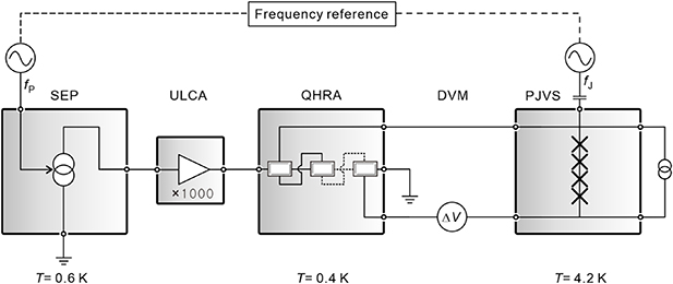
Figure 1. Experimental configuration for the SEP precision measurement. Other experimental instruments, including measurement leads between cryostats, were located in air.
Download figure:
Standard image High-resolution imageThe SEP and PJVS were simultaneously turned on and off to evaluate the Ip by the null detection technique, which enabled the offset voltage and temporal drift to be sorted from measurements. To minimize the rf heating-induced offset-voltage drift
7
, the current on/off modes were controlled by the gates located in front of two source contacts instead of being controlled by rf on/off [7, 30, 31]. The gate-induced on/off states were manipulated by alternating 0 and −0.4 V potentials to the gates while keeping rf-on (see figure S1 in the supplementary information for details (available online at stacks.iop.org/MET/57/065025/mmedia)). Consequently, Ip was determined by the following relation: [(ΔVon − ΔVoffset) − VJ]/(GULCA × RQHAR), where ΔVon and ΔVoffset are the voltage differences between VH and VJ at the on and off modes, respectively, and RQHAR is the resistance of the Hall array. GULCA, the current amplification gain of the ULCA, was calibrated using a 12-bit CCC bridge. The QHAR is traceable to the QHR standard, which will be introduced in appendix
We adopted the Josephson constant (KJ = 2e/h = 483 597.848 416 984 GHz V−1) and the von Klitzing constant (RK = h/e2 = 25 812.807 459 3045 Ω) in terms of the revised SI system based on the exact numerical values of e and h.
2.2. Characterization of the devices: SEP, Hall array, and PJVS
In this subsection, we describe the characterization of each device without connection between them. Figure 2(a) shows a scanning electron microscope image of a representative SEP with seven Schottky gates located on the surface of a GaAs/AlGaAs heterostructure, i.e. three quantum point contacts (QPCs) and one trench gate (GT) crossing the QPCs (see also figure S1(a) in the supplementary information for the optical image).
8
To operate the device, an AC voltage (or external rf signal) was applied to the entrance gate (GENT) by an rf signal generator (Keysight E8257D) to form a dynamic QD in the center of the gates by proper gate tuning, as denoted by the dashed circle [8, 32]. The number of electrons captured and transferred by the dynamic QD per each rf cycle was determined by the gate voltages. In particular, the exit-gate voltage (VEXIT) was the parameter varied to control the electron numbers once the operation condition was achieved [32]. Thus, when an AC voltage was applied to GENT, the quantized electrons were pumped from the source to the drain, satisfying the equation  . The Ip from the device was amplified with a nominal gain of 103 by the ULCA. To evaluate Ip, we converted the amplified current to a voltage using a 1 MΩ resistor in the ULCA (see figure A.1(a) in the appendix
  is expected to be approximately 56 pA. The current map shows a relatively wide n = 1 current plateau region compared with the n = 2 step. The plateau-width ratio between the steps was tuned via the gate-voltage values (see figure S2 in the supplementary information for details).
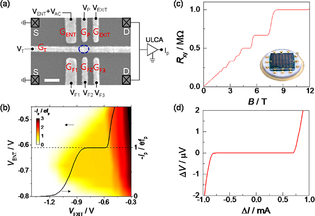
Figure 2. (a) SEM image of a GaAs/AlGaAs-based SEP with a measurement scheme to evaluate Ip by the ULCA. Scale bar is 200 nm. A quantum dot (dotted circle) is formed by properly tuning the seven Schottky gates: the trench (T), entrance (ENT), plunger (P), exit (EXIT), and boundary gates (F1, F2, and F3). S and D correspond to the source and drain, respectively. (b) Pump-current map as a function of VENT and VEXIT, where Ip was normalized by −ef with fp = 0.35 GHz (Prf = 6 dBm) and VT, F1, F2, F3, and P = 0.57, −0.41, −0.50, −0.50, and −0.64 V, respectively. Black curve: −Ip/efp as a function of VEXIT at VENT = −0.61 V, which shows a current plateau at −Ip/efp = 1, as expected. (c) Transverse resistance (Rxy) of the Hall array as a function of B field, which shows a resistance plateau at Rxy = 1 MΩ (with a filling factor ν = 2). Inset: optical-photo image of the 1 MΩ Hall array. (d) At a 90 mV step of the PJVS, the voltage difference ΔV, representing the measured voltage relative to the step voltage, as a function of the dither current ΔI.
Download figure:
Standard image High-resolution imageFigure 2(c) shows the quantized resistance plateaus of the Hall array as a function of magnetic field B with a bias current of 100 nA at T = 0.4 K, where the 1 MΩ resistance plateau corresponding to a filling factor of 2 appears for B > 8 T. The inset shows the optical image of the 1 MΩ Hall array composed of 88 Hall devices [27, 33] with a GaAs/AlGaAs heterostructure. The resistance value at B = 9.5 T was used for the precision measurements.
The JVS developed for this study is based on a 10 V programmable Josephson array. The array consists of 23 subarrays, and the output voltage of each subarray can be programmed independently through bias electronics with 24 voltage-output channels. The current bias of each subarray is supplied through a 100 Ω resistor connected to the corresponding output channel of the bias electronics. The array can output an arbitrary quantum voltage within the range ±10 V when a microwave in the range from 18 GHz to 20 GHz is irradiated into the array. The array output can be fine-tuned with the resolution of sub nano volt by setting output voltage for each subarray with the bias electronics and adjusting frequency of the microwave. Figure 2(d) shows the flatness for a 90 mV output of the PJVS. The curve in the figure represents the difference, ΔV = Vm − VJ, with respect to the dither current ΔI, where VJ and Vm are the Josephson voltage and the corresponding measured value, respectively. If a criterion ΔV = ±1 µV for flatness loss of the step is applied, the current margin of the voltage step is estimated to be approximately 1.4 mA.
3. Comparison of SEP current-induced Hall-array voltage with the Josephson voltage
3.1. Characterization of SEP with VJ = 0 V
Before the precision measurement of the SEP, we need to obtain characteristic data about the flat zone in the first current plateau as well as the system stability as a function of time. Green dots in figure 3(a) show −Ip/efp as a function of VEXIT at VENT = −0.61 V, fp = 0.350 540 506 GHz, and a nominal power, Prf = 6 dBm, in the measurement configuration shown in figure 1. The long-digit frequency was selected to minimize the difference between VH and VJ less than ∼1  10−6 V. To characterize the SEP, we set VJ = 0 V and Ip was obtained using the relation Ip = VH/(GULCA
 RQHAR)
9
where VH was measured by using a DVM (Keysight 3458A). The observed n = 1 plateau is then expected to be −56.162 781 pA. The red curve in figure 3(a) was obtained on the basis of two exponentials [34]:
RQHAR)
9
where VH was measured by using a DVM (Keysight 3458A). The observed n = 1 plateau is then expected to be −56.162 781 pA. The red curve in figure 3(a) was obtained on the basis of two exponentials [34]:


Figure 3. (a) −Ip/efp as a function of VEXIT (green dots) at VENT = −0.61 V with fp = 0.350 540 506 GHz (Prf = 6 dBm) and VT, F1, F2, F3, and P = 0.57, −0.41, −0.50, −0.50, and −0.64 V, respectively. Ip was measured using the measurement configuration shown in figure 1. The red curve is a fit-result with equation (1). (b) Open circles: |δIp| as a function of VEXIT in a semi-log scale, based on the curve in (a). Solid red curve: the fit-result with equation (1), which shows exponential curves approaching the n = 1 plateau, plotted to help identify the flat zone. Closed circles: high-resolution precision measurement data in figure 4(a), where data in the dashed box correspond to the points in the dashed box in figure 4(a). (c) Allan deviations at VEXIT = −0.65 V for the on state (green squares) and at VEXIT = −0.655 V for the on/off repetition state (red squares). Dashed and solid lines: fitting results for white-noise levels of 3.2 and 2.4  , respectively. For the fittings of the on-state and on/off state, we used relations of
  and
and  , respectively, where
  and τ are the white-noise spectral density and the measurement time, respectively. Inset: null-detection signals for the
  -on/off states, where the initial ten data points for each mode depicted by the green-colored region were rejected considering stabilization time for the ULCA.
Download figure:
Standard image High-resolution imagewhere VEXIT is related to the confining barrier height and α, β, V1, and V2 are phenomenological constants obtained by fitting the experimental data. We obtained α ≈ 60 V−1 and β ≈ 180 V−1 with a ratio of α/β = 0.33, which indicates that the thermal activation error could be dominant over the back-tunneling during the capturing stage [34]. Open circles in figure 3(b) show |δIp| as a function of VEXIT in a semi-log scale, obtained from experimental data in figure 3(a). Here, δIp is a dimensionless normalized deviation of Ip from the expected efp, defined as (Ip − efp)/efp. The red curve on the data, obtained from the red curve in figure 3(a) forms a shape similar to an inverse triangle, which empirically predicts the achievable minimum deviation, i.e. δIp ≈ 1  10−7 at VEXIT
 −0.65 V [6]. Thus, figure 3(b) also provides a VEXIT region to perform the precision measurement within δIp < 1
  10−6, which is −0.69 V < VEXIT < −0.64 V.
Green-colored points in figure 3(c) indicate the Allan deviation (σI
) for Ip on the first current plateau (at VEXIT = −0.65 V), displaying a white-noise regime to at least τ < 50 s (also see figure S3(b) for the Allan deviation at f = 0.4 GHz in the supplementary information). The solid fitting line shows the white-noise level of 3.2  , which is the same level of the SEP cryosystem alone with the ULCA (see figure A.1(b) in the appendix
3.2. Precision measurements of SEP current at two different frequencies with multiple thermal cycles
To evaluate the flatness in the selected plateau region, we used the measurement scheme based on the null-detection technique with VJ = −0.056 162 781 V or VJ = −0.063 982 914 V depending on  level to compensate the Hall voltages accordingly. In cases with no specific statement, we used 20 power line cycles for a 60 Hz power frequency with a DVM null detector, which effectively took 0.339 s per datum. We removed an internal offset error by using a function to compensate for the offset for every 3.39 s ('auto-zero once' function)
10
throughout the measurements [45, 36]. Given that the auto-zero event takes 0.58 s, obtaining 200 points of the on/off cycles in the inset of figure 3(c) takes 72.2 s. Here, we note that the time of a half cycle (∼36.1 s) is shorter than the longest sampling time during which the white noise regime holds. For each on or off mode, the first ten data points in the green-colored regions in the inset of figure 3(c) were rejected for the ULCA settling time [36], resulting in an effective time of 64.98 s for one on/off cycle. We set a waiting time of 1.5 s between the Josephson voltage switching and data acquisition from the DVM. Figure 3(c) shows the Allan deviation for this measurement (scattered red squares), which confirms that the combined measurement system is stable for at least ∼7000 s.
level to compensate the Hall voltages accordingly. In cases with no specific statement, we used 20 power line cycles for a 60 Hz power frequency with a DVM null detector, which effectively took 0.339 s per datum. We removed an internal offset error by using a function to compensate for the offset for every 3.39 s ('auto-zero once' function)
10
throughout the measurements [45, 36]. Given that the auto-zero event takes 0.58 s, obtaining 200 points of the on/off cycles in the inset of figure 3(c) takes 72.2 s. Here, we note that the time of a half cycle (∼36.1 s) is shorter than the longest sampling time during which the white noise regime holds. For each on or off mode, the first ten data points in the green-colored regions in the inset of figure 3(c) were rejected for the ULCA settling time [36], resulting in an effective time of 64.98 s for one on/off cycle. We set a waiting time of 1.5 s between the Josephson voltage switching and data acquisition from the DVM. Figure 3(c) shows the Allan deviation for this measurement (scattered red squares), which confirms that the combined measurement system is stable for at least ∼7000 s.
3.2.1. Measurements at fp = 0.350 540 506 GHz.
Figure 4(A) shows the precision measurement result, δIp, as a function of VEXIT with a type A uncertainty (uA) level of 1.2  10−6 at fp = 0.350 540 506 GHz, hereafter denoted as 0.35 GHz, and VJ = −0.056 162 781 V. Here, each data point was taken for ∼49 min, with 100 points for each on/off cycle. The data in the dashed box show a plateau region, whose 12 data are combined and averaged to give the deviation and the uncertainty, δIp ± uA = (−0.33 ± 0.37)
  10−6, as indicated by the horizontal green line with an error bar. In addition, the closed black circles in figure 3(b) were obtained from the data in figure 4(a). They qualitatively comply with the error prediction based on equation (1) that their deviations should be less than δIp = 1
  10−6. In figure 4(a), we also added the red curve obtained from the fit-result for the comparison.

Figure 4. (a) Precision measurement results, δIp, as a function of VEXIT on the first current plateau at fp = 0.350 540 506 GHz. Each data point was taken for  49 min. The data in the dashed box show a plateau region with an average deviation (horizontal green line) and a type-A uncertainty (green error bar), δIp ± uA = (−0.33 ± 0.37)
  10−6. Red curve: fitting result based on equation (1). (b) The deviations with combined uncertainties (uT) obtained at three VEXIT values for four different thermal cycles (the first cool-down process is represented by closed black circle; the second process by open purple square; the third process by closed red square; the fourth process by open blue triangle and closed green inverse triangle). The average deviation with uT for the five points in (b) including the average data in (a) is (−0.17 ± 0.27)
  10−6, as indicated by the orange horizontal line with an error bar, for a total averaging time of 36.2 h.
Download figure:
Standard image High-resolution imageFigure 4(b) shows δIp ± uT obtained over an averaging time longer than 2 h at three fixed points of VEXIT, where uT is a combined uncertainty of  and uB is a type B (systematic) uncertainty (see table 1). For example, the deviation of (0.01 ± 0.48)
  10−6 at VEXIT = −0.655 V was obtained for an ∼8 h averaging time. When we collect all of the data corresponding to the five points in figure 4(b) as well as those in figure 4(a) and run an average process corresponding to τ = 36.2 h, the statistics give (−0.17 ± 0.27)
  10−6, as denoted by the horizontal orange line with an error bar in figure 4(b).
Table 1. Uncertainty budget for the SEP currents of 56 pA and 64 pA.
| Contribution | Relative uncertainty 56 pA at 0.35 GHz (10−6) | Relative uncertainty 64 pA at 0.40 GHz (10−6) |
|---|---|---|
| Calibration of Hall array | 0.02 | 0.02 |
| Calibration of ULCA gain | 0.13 | 0.13 |
| Stability of ULCA | 0.05 | 0.05 |
| Stray voltage of ULCA input | 0.04 | 0.03 |
| Calibration of PJVS | 0.02 | 0.02 |
| DVM gain | 0.02 | 0.02 |
| Type A | 0.22 | 0.36 |
| Combined uncertainty (k = 1) | 0.27 | 0.39 |
3.2.2. Measurements at fp = 0.399 349 938 GHz.
We present another data set for a slightly varied fp of 0.399 349 938 GHz, hereafter denoted as 0.40 GHz, which confirms the robustness of the flatness of the first current plateau under a change in fp. In detail, figure 5(a) shows precision measurement results for 15–20 min-long average (scattered closed black circles) with a relative uncertainty level of ∼2  10−6 at fp = 0.40 GHz (a nominal power, Prf = 6 dBm) and VJ = 0.063 982 914 V. It provides the flat region of the plateau in the dashed-line box within ΔVEXIT = 8 mV, contrary to the ∼25 mV in figure 4(a) for fp = 0.35 GHz. The reduction of the flat region with increasing fp has been commonly observed irrespective of the device design and material [9, 32, 37]. In longer average time of a 2.5 h, the uncertainty improves to (−0.08 ± 0.76)
  10−6 at VEXIT = 27 mV (closed red squares). When the data in the dashed box are averaged, δIp ± uA = (−0.36 ± 0.51)
  10−6 is obtained, as indicated by the horizontal green line with an error bar. This deviation data is recorded in figure 5(b) at measurement sequence nm = 1 with uT. On the other hand, the data point at nm = 2 is an average value for several VEXIT values in a different measurement sequence (see figure S4 in the supplementary information). The two points in figure 5(b) give an averaged deviation with uT as (−0.33 ± 0.39)
  10−6 (a horizontal orange line and an error bar), which corresponds to τ = 9.1 h. We emphasize that our precision measurement results are reproducible within an uncertainty, despite the variation in fp. The robustness of the SEP with thermal cycles will be discussed in the following section.
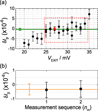
Figure 5. (a) Precision measurement of δIp on the first current plateau at fp = 0.399 349 938 GHz. Black circles represent 15–20 min-long average data, whereas the closed red square (at VEXIT = 27 mV) represents a 2.5 h-long precision measurement with a deviation of δIp ± uA = (−0.08 ± 0.76)  10−6. (b) nm = 1: average deviation with uT over the data points in the dashed box of (a); nm = 2: an average deviation for several VEXIT values with uT (see figure S4 in the supplementary information). The average deviation with uT over the two data sets gives (−0.33 ± 0.39)
  10−6 with an effective averaging time of 9.1 h (horizontal orange line with an error bar).
Download figure:
Standard image High-resolution image3.2.3. Robustness with respect to thermal cycles.
Figure 6 shows the Ip vs VEXIT curves at fp = 0.35 GHz, which were obtained over 5.3 d. Changes in the data curves were commonly observed after every 3He-condensation process, which leads to a thermal cycle between 0.55 K and 1.5 K. The changes were also observed at a fixed temperature of T = 0.55 K (see figure S5(a) in the supplement information), which are likely induced by the random telegraph noise due to repeatedly trapped and escaped electrons near the active region of the device [8, 10, 38–40]. However, even in the case where the curve changes because of the thermal cycles, the multiple curves show a common VEXIT region of the current plateau highlighted by the green-coloured region of −0.670 V < VEXIT < −0.635 V, whose precision measurement data are plotted in figure 4(b) (also see figure S5(b) in the supplementary information). The closed black circle at VEXIT = −0.655 V in figure 4(b) was obtained in the grey-curve turn in figure 6. The open purple and closed red squares at VEXIT = −0.65 V in figure 4(b) were obtained in the red-curve turn in figure 6, giving two relative deviations of (−0.24 ± 0.84)  10−6 and (−0.36 ± 0.56)
  10−6 from the nominal current values, respectively. The corresponding average times were 2.8 and 4.2 h, respectively, during the 2 d measurement process including two condensation processes. The open blue triangle and closed green inverse triangle at VEXIT = −0.645 V in figure 4(b) were obtained in the blue- and green-curve turns in figure 6, respectively. Both data were obtained for 2 d in another round of condensation. The results were almost reproducible: (−0.24 ± 0.60)
  10−6 with τ = 7.3 h and (−0.23 ± 0.60)
  10−6 with τ = 7.5 h.

Figure 6. Ip − VEXIT curves obtained at T ≈ 0.5 K (nominal) for 5.3 d. Red, blue, and green curves were recorded 2, 4, and 5.3 d after the initial measurement (grey curve) at fp = 0.350 540 506 GHz, respectively. Curve changes, as denoted by dashed circles, depended on the thermal cycles between 0.5 K and 1.5 K during the 3He-condensation process.
Download figure:
Standard image High-resolution image3.2.4. Perspective with QHRA.
One of dominant uncertainty for the present work is attributed to the calibration uncertainty of the first stage of ULCA (for the uncertainty budget, see the next section). Because the current amplification stage was calibrated by a 12-bit CCC in this work, the uncertainty is higher than the other work [35] calibrated by a 14-bit CCC. The 'bottle-neck' of uncertainty in the present configuration is attributed to the uncertainty of the current amplification gain of the first stage of ULCA, not the QHRA for a current-voltage conversion. An ideal current-to-voltage conversion with an unchangeable resistance is essential for the comparison between the converted voltage and the JVS for higher accuracy. Even though the state-of-the-art instrument of ULCA has a very stable resistance, realized by tens of precision resistors in array, this artifact resistance still cannot avoid the intrinsic time drift. Some of authors have experimentally demonstrated that a QHRA in an efficient cooling setup has practically unchangeable resistance value within the measurement uncertainty through multiple thermal cycles close to two years [27, 28]. Some of authors also demonstrated experimentally that a higher resistance value above 1 MΩ was achieved close to 10 MΩ [41]. In principle, if we have a higher-value QHRA and a higher output SEP, we can integrate SEP, QHRA and JVS in one cryostat without an ULCA. That will check the closure of the triangle in cryogenic condition with reduced uncertainty in all aspects.
4. Measurement uncertainty budget
In the precision experiment, the SEP current  was amplified by the ULCA with a nominal gain GULCA = 103. The amplified current was then applied to the 1 MΩ Hall array. The Hall voltage VH measured on the Hall array was compensated by a quantum voltage VJ from the PJVS. The residual small voltage ΔV was measured by using a DVM:
  . As described in the appendix, the current amplification gain of the input stage in the ULCA was calibrated using the CCC bridge. In table 1, the uncertainty in the calibration of ULCA gain, 0.13
  10−6, is the main contribution to the uncertainty budget. This uncertainty is due to the SQUID resolution limit in the CCC operation. The built-in temperature sensor in the ULCA simultaneously measured the temperature of the ULCA to correct the calibrated gain. The influence of temperature fluctuation ±0.01 °C on the gain was negligible. The stability of the input stage was estimated to be stable within the uncertainty of 0.05
  10−6 from the linear fitting of the calibrated data for the time span of 14 d (blue region in figure A.1(d)). The insulation resistance of the wiring cable to ground led to leakage of the SEP current. The measured insulation resistance was greater than 1
  1013 Ω at room temperature. The corresponding relative uncertainty caused by the leakage current with respect to the input of the ULCA was negligibly small (<1
  10−12). We also evaluated the leakage-current contribution to the pump current. Leakage paths are two ways: the one is via gate Schottky barrier and the other via the insulation part of the input cables to the ULCA (see section 6 in the supplementary information). Based on the measurement of the total leakage current and analysis, it turned out that it is mainly induced by the stray voltage of the ULCA through the device, whose contribution portion to Ip = 56 (64) pA is 0.04 (0.03) × 10−6. In the case of the QHAR, the invariant nature of the QHAR was confirmed through repeated thermal cycle measurements for more than 20 months [28]. The calibration uncertainty of the 1 MΩ Hall array by using the CCC was less than 20
  10−9, as described in a previous paper [27]. However, the relative deviation of RQHAR from the previous value [27] is 0.1 parts in 106, which is greater than the uncertainty. The reason for this deviation is discussed in the appendix.
The voltage difference ΔV was typically less than ±10 µV and was measured by using an 8.5-digit DVM (Keysight 3458A). The gain of the DVM was calibrated against the PJVS. The uncertainty of the gain at the 1 V range was estimated to be 2  10−8, obtained by interpolation of the measured data from −10 mV to +10 mV. Table 1 summarizes the dominant uncertainty contributions for the both SEP currents of 56 pA and 64 pA. The combined uncertainties (k = 1) for
  measurements were 0.27
  10−6 and 0.39
  10−6 for 56 pA at 0.35 GHz and 64 pA at 0.40 GHz, respectively.
5. Conclusions
In this paper, we report a precision measurement of single-electron current with QHAR and Josephson voltage. The current amplification stage of the ULCA is exploited to enlarge the small current of the SEP with a gain of 103. In our measurement setup, excess noise from various sources such as enhanced vibration and electromagnetic interference due to long signal lines connecting between the quantum devices was not sufficient to burden the combined uncertainty. The precision measurement proves that, in the revised SI, the SEP current averaged over the first plateau was equal to ef within a combined uncertainty 0.3  10−6 at Ip ≈ 60 pA.
Acknowledgments
This research was supported by Research on the 'Redefinition of SI Base Units' (KRISS-2020-GP2020-0001) funded by the Korea Research Institute of Standards and Science. The authors at NMIJ acknowledge financial support from JSPS KAKENHI (Grant Nos. JP18H05258 and JP18H01885). The quantum Hall array devices were fabricated at the AIST Nano-Processing Facility, supported by the Nanotechnology Platform Program of the Ministry of Education, Culture, Sports, Science and Technology (MEXT), Japan. The authors at KIST acknowledge financial support from an IITP grant funded by the Korean government (MSIT) (No. 20190004340011001).
M-H B performed comparison measurements and analysed the measured data. D-H C evaluated the QHAR, the gain of the current amplification stage at ULCA, and their long-term stabilities for the current-to-voltage conversion. M-S K set up the programmable JVS, provided the JVS system for the comparison and contributed to the data analysis. B-K K fabricated the SEP devices, developed the measurement program and performed the comparison measurements. S-I P and J S fabricated GaAs 2DEG wafers to be used for the SEP devices. T O and N-H K developed the 1 MΩ QHRA for the current-to-voltage conversion. N K designed the insert for the SEP cryogenics as well as the ICE cryogenic system for the QHRA evaluation. N K also designed the prototype of the KRISS pump device and initiated the KRISS QMT project. W-S K led the project and conceived the comparison experiment. M-H B, D-H C, M-S K, B-K K, N K and W-S K contributed equally to the experimental setup and the precision measurements as well as the interpretation of results. M-H B, D-H C, M-S K, and N K wrote the corresponding parts of the manuscript. M-H B and N K wrote the manuscript with extensive input and feed-back from all other authors. All authors approved the final version of the manuscript.
: Appendix A. Stability test of SEP current with ULCA
The Ip was converted to a voltage in two steps. First, the Ip was amplified by a nominal gain of 103 with the current amplification stage of the ULCA (3 GΩ/3 MΩ), as illustrated in figure A.1(a). The amplified current was then converted to a voltage by a 1 MΩ resistor. The corresponding overall transresistance-amplification gain was a nominal value of 109. Here, the current amplification gain of the ULCA was calibrated using the CCC bridge and the resistance of the resistor is traceable to the QHR standard, which will be explained in detail below. The scattered black squares in figure A.1(b) show the Allan deviation of 
 at fp = 0.40 GHz and VEXIT = 0.115 V of the inset of figure A.1(b) with a fitting result (dashed line) based on the relation
  , where
  is the white-noise spectral density. Here,
  was periodically turned on and off for 18 s for each mode to remove any offset current and temporal drift. The total measurement time was 6 h. The fitting result provides a white-noise level of
  to τ = 7000 s. This indicates that the additional noise of 2.1
  , considering the input current noise level of the ULCA of 2.4
  (see a solid line in figure A.1(b)), originates from the SEP cryo-system.
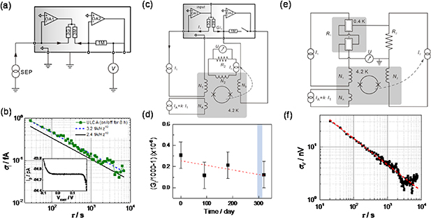
Figure A.1 (a) Measurement scheme to test the stability of SEP current with a ULCA. (b) Squares: Allan deviation of  (σI) at VEXIT = 0.115 V of the inset, as measured with a current on/off repetition process. Dashed and solid lines: fitting results with a white-noise level of 3.2 and 2.4
  , respectively. Inset: Ip − VEXIT curve at f = 0.40 GHz with Prf = 8 dBm. (c) Measurement scheme to evaluate the current amplification gain of the input state in the ULCA using the 12-bit CCC resistance bridge. (d) Dimensionless normalized deviation of the input gain from 1000 as a function of time at T = 23 °C. The blue region depicts the comparison-experiment period of 14 d. (e) Calibration scheme of the 1 MΩ Hall array with the 12-bit CCC resistance bridge and 10 kΩ resistance reference traceable to the QHR standard. (f) Squares: Allan deviation of the QHAR at 1 MΩ plateau at B = 9.5 T and T = 0.4 K (figure 2(c)). Dashed line: fitting result following the white-noise time dependence.
Download figure:
Standard image High-resolution image: Appendix B. Calibration of current amplification gain of the ULCA
The current amplification gain of the input stage in the ULCA was evaluated by the 12-bit CCC resistance bridge, as shown in figure A.1(c). The current gain was determined as follows: A current (I1) of 12.97 nA was driven in bipolar mode with a digital current source in the CCC resistance bridge via a 3 GΩ resistor and a N1(4000)-turn superconducting coil, as depicted in figure A.1(c). The maximum value for the 3 GΩ resistor was 12.97 nA because the output voltage of the operational amplifier (OA1) was ±44 V. An amplified current close to 12.97 µA was fed through a 3 MΩ resistor and a N3(4)-turn coil. The resultant magnetic flux compensates the flux generated in the 4000-turn coil. In an ideal case where the gain is exactly 103, the current ratio of I3MΩ/I3GΩ is equal to the turn ratio of 4000/4. Here, I3MΩ (I3GΩ) is the current via the 3 MΩ resistor (the 3 GΩ resistor). To evaluate a deviation from the nominal value, a coil (N2 = 1), a 10 kΩ resistance reference (R2), and an auxiliary coil (NA = 1) are configured in figure A.1(c) with the magnetic flux detected by a SQUID. Using the determined fractional turn (kNA) and the residual voltage difference across the 10 kΩ resistance reference, we determined the actual gain of the input stage of the ULCA. Figure A.1(d) shows a dimensionless normalized deviation of the input gain from 103 with T = 23 °C. The blue region of 14 d corresponds to our measurement period, which gives an average deviation of 1.21  10−7.
10−7.
: Appendix C. Calibration of the 1 MΩ Hall array for current-to-voltage conversion
The resistance value of 1 MΩ Hall array has been determined with the CCC resistance bridge in the conventional configuration by comparing it with a 10 kΩ reference resistor traceable to the QHR standard (figure A.1(e)). Numbers of turns for N1 and N2 were selected with a ratio (N1/N2) close to the nominal resistance ratio (R1/R2). An auxiliary turn (NA) was added to evaluate the effect of a deviation in the turn ratio. The magnitude and direction of currents were arranged to minimize the magnetic flux detected by a SQUID and the bridge voltage difference measured by a nanovoltmeter. The resultant fractional turn (kNA) and the average bridge voltage difference can be used to determine the resistance ratio. We thus could measure the value of the 1 MΩ Hall array. To eliminate the voltage offset and its time drift, the currents through N1, N2, and NA were simultaneously reversed. We used N1 = 4100, N2 = 41, and NA = 1. A current of 0.5 µA was driven via the 1 MΩ Hall array, leading to 0.5 V for the Hall voltage while 50 µA was applied through the 10 kΩ resistance reference. Using this approach, we obtained actual resistance value of the 1 MΩ Hall array as 999 999.843 Ω and 999 999.867 Ω before and after the measurement period, respectively. This measured Hall resistance is relatively smaller than that of a 1 MΩ Hall array in a wet 3He system by 0.1 parts in 106. This difference is attributable to inefficient cooling by energy dissipation at hot spots in the cold-finger-type 3He cryostat. In the future, the device space will be filled with 4He for efficient superfluid cooling. The scattered squares in figure A.1(f) display an Allan deviation of the QHAR measured at a 1 MΩ plateau of B = 9.5 T for 9 h with a 20 s long bipolar current cycle, which follows a time dependence of 1/ for the white noise (dashed line).
Footnotes
- 5
Kim N Re: At least 0.1 V of Hall voltage is required to be compared to the 0.1 V JVS with an uncertainty level of 10−8.
- 6
Kim N Re:
 is reserved to represent specifically the quantized current for n electrons transferred per cycle while Ip is used for more general case to represent the pumped current, the equation (1).
 - 7
Bae M Re: We note that the traditional method to control the current output by turning on and off the rf power leads to a change of temperature of the device, resulting in a change of the offset current of the device during the on/off cycle.
- 8
Bae M Re: The device was cooled with a voltage of 0.48 V applied to the seven gates to enhance the device stability.
- 9
Bae M Re: As a digital-voltmeter, an 81/2-digit commercial DVM (Keysight 3458A) was used with 20 power line cycles (PLC) for a 60 Hz power.
- 10
Bae M Re: Autozero-once function in Keysight 3458A DVM.
