Abstract
Since the new millennium coherent extreme ultra-violet and soft x-ray radiation has revolutionized the understanding of dynamical physical, chemical and biological systems at the electron’s natural timescale. Unfortunately, coherent laser-based upconversion of infrared photons to vacuum-ultraviolet and soft x-ray high-order harmonics in gaseous, liquid and solid targets is notoriously inefficient. In dense nonlinear media, the limiting factor is strong re-absorption of the generated high-energy photons. Here we overcome this limitation by generating high-order harmonics from a periodic array of thin one-dimensional crystalline silicon ridge waveguides. Adding vacuum gaps between the ridges avoids the high absorption loss of the bulk and results in a ~ 100-fold increase of the extraction depth. As the grating period is varied, each high harmonic shows a different and marked modulation, indicating their waveguiding in the vacuum slots with reduced absorption. Looking ahead, our results enable bright on-chip coherent short-wavelength sources and may extend the usable spectral range of traditional nonlinear crystals to their absorption windows. Potential applications include on-chip chemically-sensitive spectro-nanoscopy.
Introduction
In strong-field attosecond photonics, the oscillating electric field of light drives the emission of coherent short-wavelength radiation, the “high-order harmonics”, in gases1,2,3,4, liquids5, and solids6,7,8,9,10. Gas-phase high-harmonics can extend up to ~500 eV photon energies, well into the extreme ultra-violet spectral region, where they can be used for dynamical spectroscopy of physical1, chemical11, and biological12 systems. Low-pressure gases typically employed for the generation of this radiation exhibit a sufficiently low absorption at the short wavelengths (10–100 eV) that high harmonics waves generated within the gas can propagate inside the gas medium. Propagation allows the adoption of phase-matching schemes to coherently add the generated short-wavelength radiation and boost the emitted flux2,4. However, the low gas pressure requires large gas volumes inside the laser focus, limiting the development of integrated and chip-based attosecond technology. While high-density targets are beneficial at increasing the emission efficiency, they also increase absorption13,14. Ultimately, absorption prevents high harmonics to propagate inside high-density gases, liquids, and solids15, which in turn forbids coherent addition. This problem is particularly acute in solids, where absorption lengths are on the order of only few nanometers for above-bandgap high harmonics. Overcoming absorption while preserving the desirable high density may pave the way for brighter high-harmonic sources that work in the intrinsic absorption spectral region of the generating medium. Moreover, solids provide a suitable platform for photonic applications of strong-field processes, such as for petahertz electronics16,17,18, electric-field sensing19, and on-chip extreme ultra-violet microscopy. The latter requires efficient generation of high-order harmonics at the nanoscale and low-loss transport on a chip.
Using a silicon crystal as a testbed, here we demonstrate a method that overcomes absorption in the photon energy range above the minimum bandgap, for which the solid is strongly opaque, thus paving the way for coherent addition of high-harmonic waves in solids. Our method employs the nanostructured surface sketched in Fig. 1. It consists of a periodic array of thin single-crystal silicon ridge-waveguides that are intended to spatially separate the nonlinear high-harmonic polarization, which travels along the ridge’s sidewalls, from the generated high-harmonic waves, which leak and propagate inside the vacuum slots between ridges. Generating high harmonics in the ridge-vacuum interface region (step 1) allows their coupling into the vacuum slots (step 2) and their propagation to the output of the crystal (step 3). The width of individual silicon ridge-waveguides is designed to be sub-wavelength in order to maintain a relatively high field strength on the ridges’ sidewalls, similarly to slot waveguides20. However, contrary to slot waveguides, our device is nonlinear, utilizes the ridges’ sidewalls as the active high-harmonic-emission elements and operates at photon energies for which bulk Si is opaque. Although the excitation field spreads out throughout the structure similarly to slot-waveguides20 (see Supplementary Note 1 for modeling of the infrared field distribution), the high-harmonic mode is confined inside each slot (and thus each slot is independent from the others) due to strong absorption inside each ridge. In this case, each vacuum slot can be viewed as a ‘lossy’ waveguide for harmonic emission. Our approach exploits the desired high density of crystals and the low loss of the vacuum channels, which constitute leaky waveguides for the high harmonics. Unlike previous reports of enhanced high-harmonic emission from solids that utilize nanoscale confinement of the infrared field21,22,23,24, our structures make use of both the increased surface area around each waveguide and the reduced absorption. Beating the absorption limit of bulk opens the possibility for on-chip guiding of above-gap high harmonics and for developing crystals that exploit high intrinsic perturbative nonlinearities in the crystal’s absorption bands. The method can potentially be adapted to other wide bandgap solids, liquids, as well as high-pressure gases.
Cross-section of the designed grating structures composed of thin Si ridges, illuminated from left to right with an intense (~0.2 TW/cm2 in vacuum) infrared laser field. The thin vertical red line represents the sapphire/Si interface. The infrared intensity simulated with Finite-Differences Frequency Domain (FDFD), color coded, is highest on the ridges’ sidewalls, where high-harmonic generation preferentially takes place (step 1). Generation of high-harmonics within one absorption length of bulk Si (~5 nm) from the Si-vacuum interface allows coupling of the generated high-harmonics inside the vacuum slot (step 2), followed by their propagation and coherent addition in the slot (step 3). An illustration of the emitted high harmonics is superimposed in purple.
Results and discussions
We report two main findings. First, as the slot width is varied, each deep- and vacuum-ultraviolet high harmonic shows strong modulations unique to each harmonic, indicating the guiding of the generated short-wavelength radiation in the vacuum channels, as well as the onset of coherent addition on otherwise absorption-limited radiation13,15. Second, increasing the guiding distance yields a monotonic buildup of high harmonics over a distance of ~700 nm, indicating a ~100-fold increase of transmission with respect to bulk Si (Labs ~5 nm). Despite the reduced amount of material and phase mismatch, the measured high-harmonic flux is comparable or even exceeds that measured from uniform bulk. It may even be improved with the adoption of phase-matching schemes.
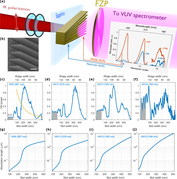
In the experiment (Fig. 2a), we illuminate linearly tapered gratings consisting of 1-μm-tall Si ridges of continuously varying pitch with TM-polarized (magnetic field pointing parallel to the ridges) mid-infrared few-cycle femtosecond pulses with a center wavelength of 2.35 μm at a repetition rate of 80 MHz [25]. The estimated peak intensity in vacuum is ~0.2 TW/cm2. The generated high-harmonics are collected with a Fresnel zone plate (FZP) and their spectrum is recorded with a vacuum-ultraviolet (VUV) spectrometer and a silicon CCD camera (see “Methods” section for details on the experimental setup and fabrication). The taper of the gratings is sufficiently small (the slot width varies by ~0.2 nm/μm) that the geometry variation within the laser focus is negligible. Varying the grating geometry by translating the structures along the taper (laterally with respect to the laser focus) results in variations of the high-harmonic spectrum, as shown in the inset of Fig. 2a for illumination of two sample regions with narrow (blue) and wide (red) slot widths. Figure 2b shows a high-resolution image of the end of the gratings, on the wide slot side.
a Sketch of the experimental apparatus. Linearly polarized mid-infrared femtosecond laser pulses (IR, red beam) are focused on a chirped grating structure composed of Si ridges with continuously varying width and pitch, fabricated on a sapphire substrate. Different geometries are explored by translating the grating laterally to the beam propagation axis. A combination of a half-wave plate (L/2, before) and a quarter-wave plate (L/4, after) are used to compensate for the birefringence of the sapphire substrate, assuring that the polarization entering the grating structure is linear and oriented transverse magnetic (TM). The generated high-harmonics (purple beam) are collected with a custom-made fresnel zone plate (FZP) and focused on the input slit of a vacuum ultra-violet (VUV) spectrometer. See “Methods section” for details on the experimental setup. (a, inset) High-harmonic (HH) spectra recorded for two geometries: 180 nm slot width and 160 nm ridge width (blue line), 360 nm slot width and 110 nm ridge width (red line). b Scanning electron image of the end of the Si gratings. Scale bar is 500 nm (plane view). c–f Measured high-harmonic power (blue lines) for harmonics 9th to 15th (respectively c–f), as a function of the slot (bottom axis) and ridge (top axis) widths. The gray-shaded area corresponds to bulk Si. The observed order-dependent modulation occurs despite the monotonic decrease of the infrared field strength at the sidewalls of the Si ridges (yellow dash-dotted line in panel c, simulated with Finite-Differences Frequency Domain and scaled by an arbitrary factor to show the trend). g–j Calculated absorption lengths for the grating structures. For narrow slot widths, the short absorption length (Labs, blue line) of the leaky slot mode limits the transmitted high-harmonic power to the intrinsic absorption limit of the bulk crystal (~5 nm). As the slot width widens beyond approximately one harmonic wavelength, transmission significantly increases compared to bulk.
Finely scanning the slot widths results in strongly modulated high-harmonic powers, as reported in Fig. 2c–f, blue lines, for harmonics 9th to 15th. Due to fabrication constraints, the ridge width also changes (top axis). The gray-shaded areas result from illumination of bulk Si. Each high harmonic shows a marked modulation with slot width which is unique to each harmonic order. Similar results from thicker-ridge gratings are presented in Supplementary Note 4. The observed harmonic-order dependent, non-monotonic modulation suggests the guiding of high harmonics and the onset of propagation effects over distances much longer than the intrinsic propagation length in bulk Si (on the order of one absorption length, ~5 nm). This is our major experimental finding that corroborates the working principle presented in Fig. 1. At the same time, the simulated intensity of the infrared field on the Si ridges’ sidewalls (dashed yellow lines in Fig. 2c) exhibits a monotonic decrease as the slot width increases (see Supplementary Note 1). This would result in a simultaneous decrease of all harmonics without the vacuum propagation effects. Additional arguments that indicate the order-dependent modulation is due to guiding effects rather than to variations of the excitation field strength and polarization can be made based on the measured power scaling of high harmonics and their dependence on the ellipticity of the infrared field. This discussion is included in Supplementary Note 3. Towards the wide-slot end of the grating, the measured harmonic power decreases for all reported orders, likely due to the decay of the infrared field (Fig. 2c, dashed yellow line).
Analytical analysis of the propagation of harmonic waves in the leaky slot (see Supplementary Note 2 for details about the theoretical framework) reveals a sharp increase of transmission for slot widths comparable to one harmonic wavelength, as the blue lines in Fig. 2g–j show. This sharp increase is consistent with the maximum measured high-harmonic flux occurring for slot widths comparable to or larger than one harmonic wavelength.
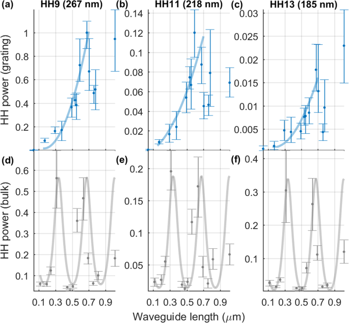
Reduced absorption implies that high-harmonic yield builds up over long distances. To measure the buildup, we record high-harmonic spectra from a series of gratings of varying length, at a fixed slot width of 500 nm. The results are shown in Fig. 3a–c. A monotonic increase of flux is observed up to an optimum guiding distance of ~700 nm, which is >100 times longer than the intrinsic absorption length of bulk Si (~5 nm for the measured harmonics). According to our model, we expect the guiding distance to depend on harmonic order for narrower slot widths, decreasing for decreasing slot width, because narrower slots force more bounces off the sidewalls, each bounce contributing loss. The increase of the guiding distance is our second experimental finding. As a control experiment, we measure the high-harmonic yield on un-patterned Si films as a function of the film thickness, as shown in Fig. 3d–f. The bulk signal shows large and sharp modulations determined by Fabry-Perot resonances in the film, without any signature of buildup even down to the thinnest measured film (120 nm), i.e. the buildup of high-harmonic flux is already saturated, as expected from the short absorption length.
The high-harmonic power emitted from the grating (panels a–c, “HH” is the high harmonic order) monotonically increases for waveguide lengths up to ~700 nm, evidencing the coherent buildup over distances much longer than the intrinsic absorption length of Si (~5 nm). In contrast, the flux measured from an unstructured Si film (panels d–f) shows sharp oscillations due to the modulation of the infrared field strength by Fabry-Perot interference, i.e., without coherent buildup down to the thinnest measured film (115 nm). The blue lines are a guide to eye. The gray lines represent the square of the expected Fabry-Perot transmission of Silicon-On-Sapphire, where the square is taken to account for the nonlinearity. Error bars are 95% confidence interval obtained from multiple measurements on various regions across the same grating (of nominal constant guiding length).
An immediate advantage of exploiting the high transmission of the slots is that the high-harmonic flux can potentially outperform that from bulk crystals. Unlike previously reported field-enhancing nanostructures21,22,23,24, where the high-harmonic enhancement only appears at low excitation intensities, here we show that with reduced absorption we can enhance the high-harmonic flux at high intensities up to the material breakdown. Figure 4 shows the high-harmonic yield as a function of infrared power, until damage occurs, indicated by a sudden drop in the yield. Despite phase mismatch and the ~3 times less amount of nonlinear material, the device outperforms or matches bulk for almost all harmonics. A decrease of the gain for increasing harmonic order may be due to higher sensitivity to the slot geometry and sidewall roughness, as well as to an increased confinement of the high-harmonics inside the slot – thus reducing overlap with the nonlinear polarization at the sidewalls.
The power of high harmonics 9 through 15 (panels a–d) from gratings (red lines) and bulk Si (blue lines) increases monotonically with the infrared power, regardless of the order, up to the onset of damage, marked by the sharp decrease. “HH” denotes the high-harmonic order. The red lines pertain the structures presented in Fig. 2. Each red curve is acquired at a geometry that maximizes the high-harmonic power in Fig. 2c–f. The gratings damage at ~20% lower power than the bulk. Error bars have been added at one point for each curve for illustrative purposes. The error is 95% confidence interval obtained from the data acquired above the damage threshold. The error mostly represents fluctuations in laser intensity.
Conclusions
To conclude, we have overcome one of the major obstacles towards high-flux solid-state high-harmonic sources: the extremely short absorption length of bulk solids at photon energies above their minimum bandgap, where the strong absorption (Labs ~5 nm) ultimately limits the overall harmonic yield and solid-state based attosecond technologies. We have done so by generating high harmonics at the surface of a nanostructured silicon crystal, resulting in a ~100-fold increase in extraction depth. Our results suggest that it will be possible to extend nanophotonic devices that rely on propagating waves for applications that benefit from short-wavelength radiation, such as on-chip chemically sensitive spectroscopy and nanoscale imaging. For example, tailoring the dispersion with sub-infrared-wavelength structures25,26 and photonic crystals27 may lead to phase-matched or quasi-phase matched28 efficient nanoscale high-harmonic emission. Short-wavelength on-chip laser oscillators and frequency combs can potentially be realized too, for example, by adapting slot-waveguide-based ring resonators29. Adiabatic phase matching also promises to convert infrared to high-harmonic power with near unity efficiency30. While we demonstrate this concept specifically in silicon, the approach can be generalized to other solids with wide bandgaps. For example, wide bandgap crystals amenable to nanofabrication, such as lithium niobate31 and quartz, and suitable for emission of extreme ultra-violet wavelengths, can potentially replace Si, thus pushing nanoscale sources to shorter wavelengths still. Finally, the same concepts can be applied to liquid- and high-pressure gas-phase high-harmonic generation, which also suffer from the small absorption length5,14, at even shorter wavelengths. Micro-to-nanoscale patterning of liquids can be achieved with the help of microfluidic chips32, and gas volumes can potentially be manipulated too if adsorbed on patterned surfaces. Therefore, we expect our findings have a potentially broad impact on optimizing a wide range of coherent short-wavelength sources. The method is also compatible with MHz-rate pumping33 and thus provides a means for higher-flux frequency combs at short wavelengths.
Methods
Experiment setup
The laser source used in this experiment is a mid-infrared femtosecond high-repetition-rate master oscillator power amplifier (MOPA) based on a Cr2+:ZnS gain medium. The MOPA delivers three-cycle pulses (26 fs) with a central wavelength of 2.35 μm at 80 MHz repetition rate, with maximum pulse energy 79 nJ. The output power of the MOPA is controlled by a half-wave plate combined with a germanium mirror placed at Brewster’s angle. The reflected linearly polarized beam from the germanium mirror is sent into the experiment vacuum chamber. The chamber is kept at a pressure of ~2 × 10⁻² mbar to avoid air absorption of ultraviolet radiation. The beam is focused onto the sample at normal incidence from the sapphire substrate side via an off-axis parabolic mirror with f/1.2, resulting in a beam diameter of 13 μm 1/e2 at the focus. We estimate that between ~25 and ~45 lines of the grating are illuminated within the beam diameter. The spectrum coupled to the structure is expected to be as broad as the laser bandwidth (see Supplementary Fig. 2). A half-wave and a quarter-wave plate are placed before the chamber entrance to compensate the rotation of the polarization state of the excitation pulse in the birefringent sapphire substrate. The transmitted high harmonics are collected with a NA = 0.15 Fresnel zone plate (FZP) consisting of 0.5-µm-thick Si zones on a sapphire substrate. The FZP is fabricated in-house. The Si acts as an intensity mask for the harmonics, given that it is thicker than the absorption length of the harmonics reported. The FZP is designed to transmit the center portion of the high-harmonic beam (center-pass) to increase the transmissivity. The FZP focuses the harmonics onto the entrance slit of a VUV spectrometer (McPherson, model 234), equipped with a 1200-l/mm Al-coated grating. Given the low NA of the FZP compared to the estimated diffraction angle of the high harmonics from the gratings (>20° for the 13th harmonic at the widest grating pitch), only the 0th order should be collected by the FZP. The spectrally separated harmonics after the spectrometer are imaged with a Si CCD (Andor, model DO-420-BN). The far-field profile of the high-harmonic beam is discussed in Supplementary Note 5 and shown in Supplementary Fig. 7. Due to slight chromatic dispersion of the FZP, its position is optimized for each harmonic order.
Fabrication
Grating structures presented in Fig. 2 are fabricated using a Si-on-sapphire wafer, with a nominal 1-μm-thick Si film and 460-μm-thick sapphire substrate. A JEOL JBX-6300FS electron-beam lithography system is used to pattern a 400-nm-thick FOX-16 electron-beam resist layer spun on Si surface. After e-beam lithography, a plasma etcher is used to transfer the pattern and etch through Si with BCl3/Cl2/O2 chemistry. After etching, the exposed resist mask is stripped in HF.
The original design of the grating structure is 2 mm long and the width of the individual vacuum slot is linearly tapered from 50 nm to 500 nm over the total length. However, during electron-beam exposure, the narrow slot width side of the grating is over exposed due to proximity effect. The resist in the overexposed area forms a uniform oxide mask on Si and eventually leaves an area of unstructured Si film at the narrow side of the grating after etching, which is used to benchmark the bulk emission in the optical measurement. For the same reason, widening slot widths result is reduced exposure of the ridges, and ultimately to a continuous thinning of the ridge’s width as the slot widens. This continuous variation of the ridges’ width is reported in the top axis of Fig. 2c–f and Supplementary Fig. 5.
After optical measurement, a few-nm thick of Au/Pd (60:40 ratio) layer is deposited on the structures for SEM imaging.
The same procedure is adopted to fabricate a center-pass Fresnel zone plate with 0.15 Numerical Aperture on a Si-on-sapphire 10 × 10 mm piece, with a nominal 500-nm-thick Si film and 460-μm-thick sapphire substrate.
For Fig. 3, a 4″ SOS wafer is spun with ZEP520-A e-beam resist, and a pattern of a series of identical 50 × 50 μm2 gratings with a fixed ridge width of 160 nm and a slot width of 500 nm is written with the same JEOL system. After development of the pattern, a first etch is performed to transfer the pattern to the (nominally) 1-μm-thick Si film. After stripping the residual resist, the wafer is spun with a thick protective photoresist (~ a few microns) and the gratings are diced to individual pieces. Finally, each piece is etched for different times to obtain gratings of varying length. The height of the gratings is measured with AFM equipped with a high-aspect ratio tip (AR5-NCHR-10 from Nanosensors). For the high-harmonic measurements presented in Fig. 3, the FZP was removed.
Data availability
The datasets generated and/or analyzed during the current study are available from the corresponding author on reasonable request.
References
Krausz, F. & Ivanov, M. Attosecond physics. Rev. Mod. Phys. 81, 163–234 (2009).
Takahashi, EijiJ. et al. Coherent water window x ray by phase-matched high-order harmonic generation in neutral media. Phys. Rev. Lett. 101, 253901 (2008).
Popmintchev, T. et al. Bright coherent ultrahigh harmonics in the keV X-ray regime from mid-infrared femtosecond lasers. Science 336, 1287–1291 (2012).
Cardin, V. et al. Self-channelled high harmonic generation of water window soft x-rays. J. Phys. B Mol. Opt. Phys. 51, 174004 (2018).
Luu, T. T. et al. Extreme–ultraviolet high–harmonic generation in liquids. Nat. Commun. 9, 3723 (2018).
Ghimire, S. et al. Observation of high-order harmonic generation in a bulk crystal. Nat. Phys. 7, 138–141 (2011).
Ndabashimiye, G. et al. Solid-state harmonics beyond the atomic limit. Nature 534, 520–523 (2016).
Luu, T. T. et al. Extreme ultraviolet high-harmonic spectroscopy of solids. Nature 521, 498–502 (2015).
Vampa, G. et al. Linking high harmonics from gases and solids. Nature 522, 462–464 (2015).
Hohenleutner, M. et al. Real-time observation of interfering crystal electrons in high-harmonic generation. Nature 523, 572–575 (2015).
Kraus, P. M. et al. The ultrafast X-ray spectroscopic revolution in chemical dynamics. Nat. Rev. Chem. 2, 82–94 (2018).
Calegari, F. et al. Ultrafast electron dynamics in phenylalanine initiated by attosecond pulses. Science 346, 336–339 (2014).
Constant, E. et al. Optimizing high harmonic generation in absorbing gases: Model and experiment. Phys. Rev. Lett. 82, 1668 (1999).
Takahashi, E., Nabekawa, Y. & Midorikawa, K. Generation of 10-µJ coherent extreme-ultraviolet light by use of high-order harmonics. Opt. Lett. 27, 1920–1922 (2002).
Ghimire, S. et al. Generation and propagation of high-order harmonics in crystals. Phys. Rev. A 85, 043836 (2012).
Garg, M. et al. Multi-petahertz electronic metrology. Nature 538, 359–363 (2016).
Schiffrin, A. et al. Optical-field-induced current in dielectrics. Nature 493, 70–74 (2013).
Higuchi, T. et al. Light-field-driven currents in graphene. Nature 550, 224–228 (2017).
Vampa, G. et al. Strong-field optoelectronics in solids. Nat. Photon. 12, 465–468 (2018).
Almeida, V. R., Xu, Q., Barrios, C. A. & Lipson, M. Guiding and confining light in void nanostructure. Opt. Lett. 29, 1209–1211 (2004).
Han, S. et al. High-harmonic generation by field enhanced femtosecond pulses in metal-sapphire nanostructure. Nat. Commun. 7, 13105 (2016).
Vampa, G. et al. Plasmon-enhanced high-harmonic generation from silicon. Nat. Phys. 13, 659–662 (2017).
Sivis, M. et al. Tailored semiconductors for high-harmonic optoelectronics. Science 357, 303–306 (2017).
Liu, H. et al. Enhanced high-harmonic generation from an all-dielectric metasurface. Nat. Phys. 14, 1006 (2018).
Piggott, A. Y. et al. Inverse design and demonstration of a compact and broadband on-chip wavelength demultiplexer. Nat. Photon. 9, 374–377 (2015).
Cheben, P. et al. Subwavelength integrated photonics. Nature 560, 565–572 (2018).
Corcoran, B. et al. Green light emission in silicon through slow-light enhanced third-harmonic generation in photonic-crystal waveguides. Nat. Photon. 3, 206–210 (2009).
Yu, S.-P. et al. Nanowire photonic crystal waveguides for single-atom trapping and strong light-matter interactions. Appl. Phys. Lett. 104, 111103 (2014).
Barrios, C. A. & Lipson, M. Electrically driven silicon resonant light emitting device based on slot-waveguide. Opt. Express 13, 10092–10101 (2005).
Suchowski, H., Oron, D., Arie, A. & Silberberg, Y. Geometrical representation of sum frequency generation and adiabatic frequency conversion. Phys. Rev. A 78, 063821 (2008).
Wang, C. et al. Monolithic lithium niobate photonic circuits for Kerr frequency comb generation and modulation. Nat. Commun. 10, 978 (2019).
Schmidt, H. & Hawkins, A. R. The photonic integration of non-solid media using optofluidics. Nat. Photon. 5, 598–604 (2011).
Vampa, G. et al. Characterization of high-harmonic emission from ZnO up to 11 eV pumped with a Cr: ZnS high-repetition-rate source. Opt. Lett. 44, 259–262 (2019).
Acknowledgements
This works is supported by the W. M. Keck Foundation and Stanford University. Part of this work was performed at the Stanford Nano Shared Facilities (SNSF), supported by the National Science Foundation (NSF) under award ECCS-1542152, and in the nano@Stanford labs, which are supported by NSF as part of the National Nanotechnology Coordinated Infrastructure under award ECCS-1542152. The authors thank the Stanford Photonic Research Center and IPG Photonics for equipment gifts, R. Coffee for equipment loans, J. Vavra for equipment loans and discussions, and A. Sakdinawat and K. Lee for helping with the FZP fabrication.
Author information
Authors and Affiliations
Contributions
H.L. and G.V. contributed equally. H.L. and G.V. designed the nanostructures and carried out the high-harmonic experiments. H.L., G.V., and J.L.Z. fabricated the structures. Y.S. and S.B. contributed to the simulations. J.V., S.F., P.H.B., and D.A.R. supervised the work. All authors contributed to the manuscript.
Corresponding author
Ethics declarations
Competing interests
The authors declare no competing interests.
Additional information
Publisher’s note Springer Nature remains neutral with regard to jurisdictional claims in published maps and institutional affiliations.
Supplementary information
Rights and permissions
Open Access This article is licensed under a Creative Commons Attribution 4.0 International License, which permits use, sharing, adaptation, distribution and reproduction in any medium or format, as long as you give appropriate credit to the original author(s) and the source, provide a link to the Creative Commons license, and indicate if changes were made. The images or other third party material in this article are included in the article’s Creative Commons license, unless indicated otherwise in a credit line to the material. If material is not included in the article’s Creative Commons license and your intended use is not permitted by statutory regulation or exceeds the permitted use, you will need to obtain permission directly from the copyright holder. To view a copy of this license, visit http://creativecommons.org/licenses/by/4.0/.
About this article
Cite this article
Liu, H., Vampa, G., Zhang, J.L. et al. Beating absorption in solid-state high harmonics. Commun Phys 3, 192 (2020). https://doi.org/10.1038/s42005-020-00472-5
Received:
Accepted:
Published:
DOI: https://doi.org/10.1038/s42005-020-00472-5
Comments
By submitting a comment you agree to abide by our Terms and Community Guidelines. If you find something abusive or that does not comply with our terms or guidelines please flag it as inappropriate.

