Influence of Hot Carrier and Thermal Components on Photovoltage Formation across the p–n Junction

 ,
,  ,
, 
Abstract
:1. Introduction
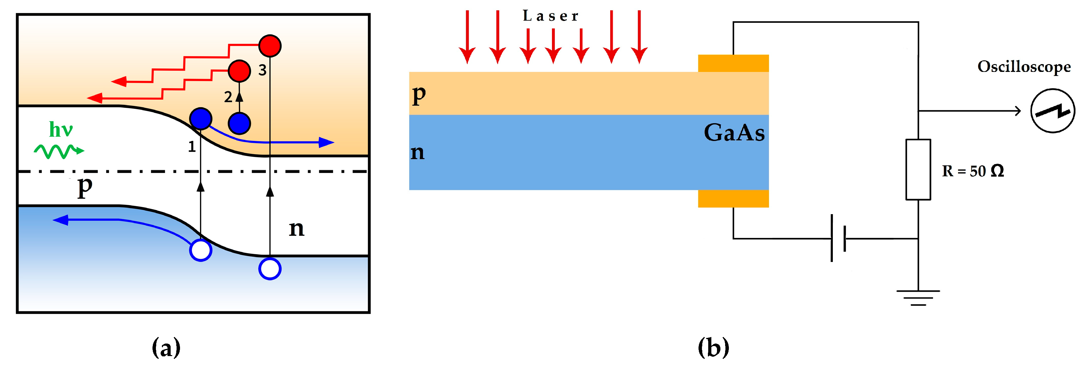
2. Experimental
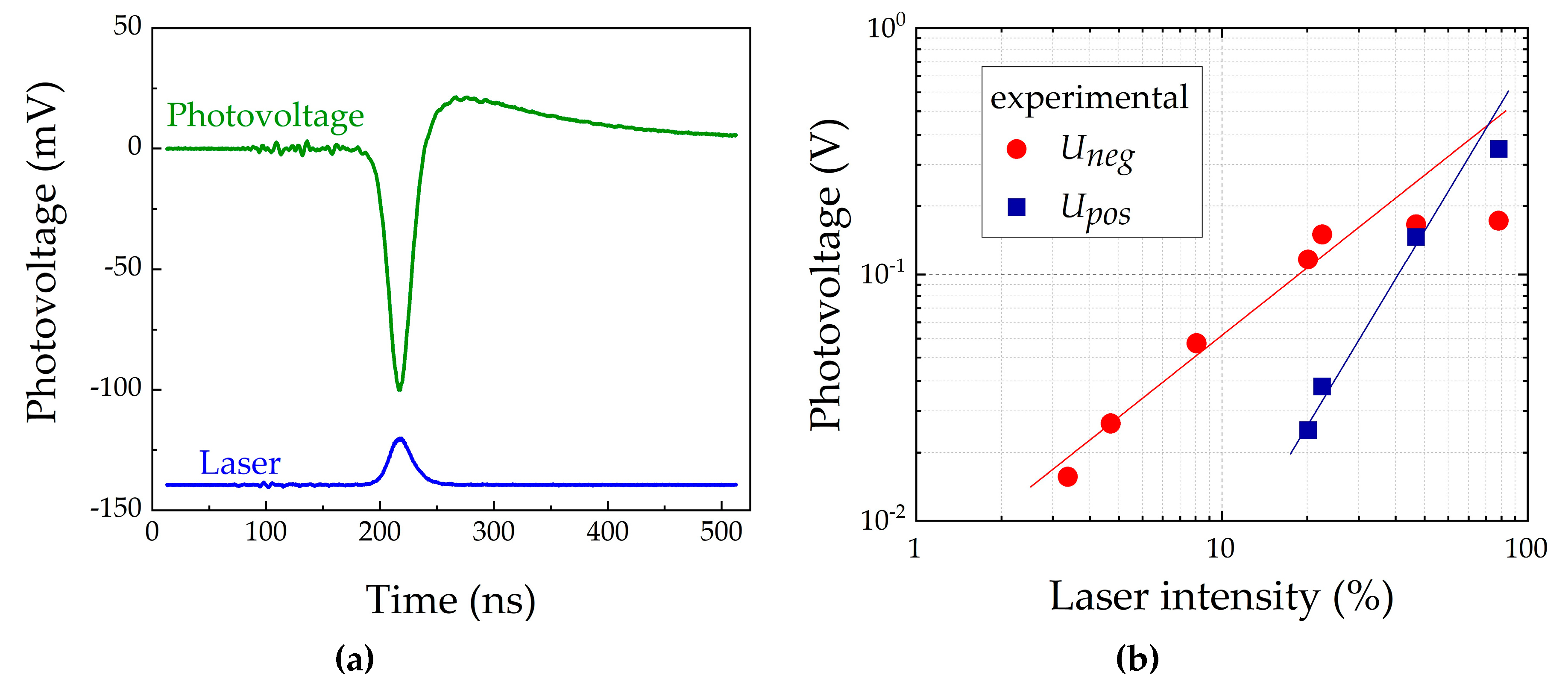
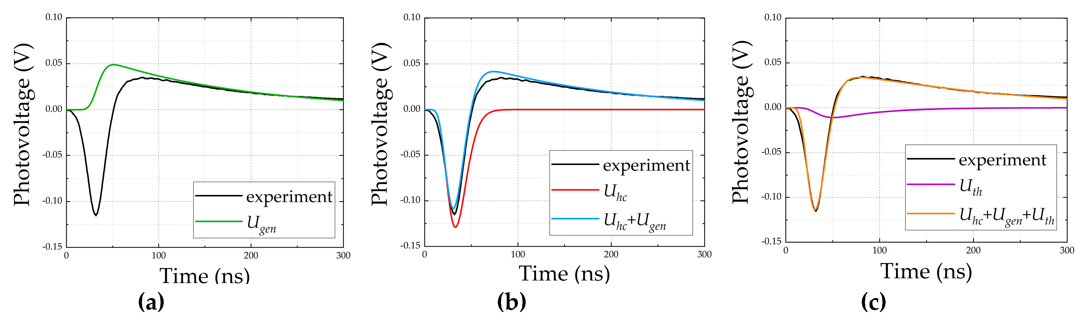
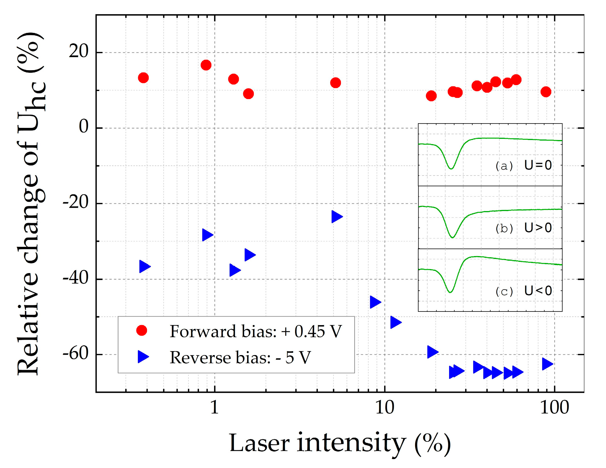
3. Results
4. Conclusions
Author Contributions
Funding
Conflicts of Interest
References
- Shockley, W.; Queisser, H. Detailed Balance Limit of Efficiency of p--n Junction Solar Cells. J. Appl. Phys. 1961, 32, 510–519. [Google Scholar] [CrossRef]
- Hirst, L.C.; Ekins-Daukes, N.J. Fundamental losses in solar cells. Prog. Photovolt. Res. Appl. 2011, 19, 286–293. [Google Scholar] [CrossRef]
- Ruhle, S. Tabulated values of the Shockley–Queisser limit for single junction solar cells. Sol. Energy 2016, 130, 139–147. [Google Scholar] [CrossRef]
- Nelson, C.A.; Monahan, N.R.; Zhu, X.-Y. Exceeding the Shockley–Queisser limit in solar energy conversion. Energy Environ. Sci. 2013, 6, 3508–3519. [Google Scholar] [CrossRef]
- Goodnick, S.; Honsberg, C. Modeling carrier relaxation in hot carrier solar cells. In Proceedings of the Physics, Simulation, and Photonic Engineering of Photovoltaic Devices, San Francisco, CA, USA, 23–26 January 2012; pp. 82560W-0–82560W-10. [Google Scholar]
- Konovalov, I.; Plos, B. Modeling of hot carrier solar cell with semi-infinite energy filtering. Sol. Energy 2019, 185, 59–63. [Google Scholar] [CrossRef]
- Hirst, L.C.; Fujii, H.; Wang, Y.; Sugiyama, M.; Ekins-Daukes, N.J. Hot carriers in quantum wells for photovoltaic efficiency enhancement. IEEE J. Photovoltaics 2014, 4, 244–252. [Google Scholar] [CrossRef]
- Tsai, C.-Y. Theoretical model and simulation of carrier heating with effects of nonequilibrium hot phonons in semiconductor photovoltaic devices. Prog. Photovolt. Res. Appl. 2018, 26, 1–17. [Google Scholar] [CrossRef]
- Hirst, L.C.; Walters, R.J.; Fuhrer, M.F.; Ekins-Daukes, N.J. Experimental demonstration of hot-carrier photo-current in an InGaAs quantum well solar cell. Appl. Phys. Lett. 2014, 104, 231115–231119. [Google Scholar] [CrossRef]
- Kamide, K. Current–voltage curves and operational stability in hot-carrier solar cell. J. Appl. Phys. 2020, 127, 183102–183118. [Google Scholar] [CrossRef]
- Wang, G.; Liao, L.P.; Elseman, A.M.; Yao, Y.Q.; Lin, C.Y.; Hu, W.; Liu, D.B.; Xu, C.Y.; Zhou, G.D.; Li, P.; et al. An internally photoemitted hot carrier solar cell based on organic-inorganic perovskite. Nano Energy 2020, 68, 104327–104383. [Google Scholar] [CrossRef]
- Ašmontas, S.; Gradauskas, J.; Seliuta, D.; Sužiedėlis, A.; Valušis, G.; Širmulis, E. Fast infrared detectors based on nonuniform semiconductors. In Proceedings of the Advanced Optical Devices, Technologies, and Medical Applications, Bellingham, WA, USA, 18–22 August 2003; pp. 221–230. [Google Scholar]
- Ašmontas, S.; Maldutis, E.; Širmulis, E. CO2 Laser radiation detection by carrier heating in inhomogeneous semiconductors. Int. J. Optoelectron. 1988, 3, 263–266. [Google Scholar]
- Ašmontas, S.P.; Gradauskas, J.; Seliuta, D.; Širmulis, E. Photoresponse in nonuniform semiconductor junctions under infrared laser excitation. In Proceedings of the Fourth International Conference on Material Science and Material Properties for Infrared Optoelectronics, Kiev, Ukraine, 29 September–2 October 1998; pp. 125–131. [Google Scholar]
- Umeno, M.; Sugito, Y.; Jimbo, T.; Hattori, H.; Amenixa, Y. Hot photo-carrier and hot electron effects in p-n junctions. Sol. St. Electron. 1978, 21, 191–195. [Google Scholar] [CrossRef]
- Andrianov, A.V.; Valov, P.M.; Sukhanov, V.L.; Tuchkevich, V.V.; Shmidt, N.M. Photoeffect on silicon p–n junction under intraband carriers heating by light. Phys. Techn. Poluprovodn. 1980, 14, 859–864. [Google Scholar]
- Encinas-Sanz, F.; Guerra, J.M. Laser-induced hot carrier photovoltaic effects in semiconductor junctions. Prog. Quantum Electron. 2003, 27, 267–294. [Google Scholar] [CrossRef]
- Ašmontas, S.; Gradauskas, J.; Seliuta, D.; Širmulis, E. Photoelectrical properties of nonuniform semiconductor under infrared laser radiation. In Proceedings of the Nonresonant Laser-Matter Interaction (NLMI-10), St. Petersburg, Russia, 21–23 August 2000; pp. 18–27. [Google Scholar]
- Ašmontas, S.; Gradauskas, J.; Sužiedėlis, A.; Šilėnas, A.; Širmulis, E.; Švedas, V.; Vaičikauskas, V.; Vaičiūnas, V.; Valiulis, D.; Žalys, O.; et al. Peculiarities of photovoltage formation across p-n junction under illumination of laser radiation. Solid State Phenom. 2017, 267, 167–171. [Google Scholar]
- Ašmontas, S.; Gradauskas, J.; Sužiedėlis, A.; Šilėnas, A.; Širmulis, E.; Švedas, V.; Vaičikauskas, V.; Žalys, O. Hot carrier impact on photovoltage formation in solar cells. Appl. Phys. Lett. 2018, 113, 071103–071106. [Google Scholar] [CrossRef]
- Ašmontas, S.; Gradauskas, J.; Naudjyus, K.; Širmulis, E. Photoresponse of InSb-based p-n structures during illumination by a CO2 laser. Semiconductors 1994, 28, 1089–1091. [Google Scholar]
- Ašmontas, S.; Gradauskas, J.; Seliuta, D.; Sužiedėlis, A.; Širmulis, E.; Valušis, G.; Tetyorkin, V.V. CO2 Laser Induced Hot Carrier Photoeffect in HgCdTe. Mater. Sci. Forum 2002, 384–385, 147–150. [Google Scholar]
- Kempa, K.; Naughton, M.J.; Ren, Z.F.; Herczynski, A.; Kirkpatrick, T.; Rybczynski, J.; Gao, Y. Hot electron effect in nanoscopically thin photovoltaic junctions. Appl. Phys. Lett. 2009, 95, 233121–2331214. [Google Scholar] [CrossRef] [Green Version]
- Hurlbut, W.C.; Lee, Y.-S.; Vodopyanov, K.L.; Kuo, P.S.; Fejer, M.M. Multiphoton absorption and nonlinear refraction of GaAs in the mid-infrared. Opt. Lett. 2007, 32, 668–670. [Google Scholar] [CrossRef]
- Won, W.; Yang, Y.; Chang, T.G.; Song, I.H.; Cho, Y.S.; Heo, J.; Jeon, W.G.; Lee, J.W.; Kim, J.K. Input-Output Relationship of LinearTime-Invariant (LTI) System. In Signals and Systems with MATLAB; Springer: Berlin/Heidelberg, Germany, 2009; pp. 15–17. [Google Scholar]
- Glover, G.H. Study of electron energy relaxation times in GaAs and InP. J. Appl. Phys. 1973, 44, 1295–1301. [Google Scholar] [CrossRef]
- Sasaki, M.; Negishi, H.; Inoue, M. Pulsed laser--induced transient thermoelectric effects in silicon crystals. J. Appl. Phys. 1986, 59, 796–802. [Google Scholar] [CrossRef]


Publisher’s Note: MDPI stays neutral with regard to jurisdictional claims in published maps and institutional affiliations. |
© 2020 by the authors. Licensee MDPI, Basel, Switzerland. This article is an open access article distributed under the terms and conditions of the Creative Commons Attribution (CC BY) license (http://creativecommons.org/licenses/by/4.0/).
Share and Cite
Gradauskas, J.; Ašmontas, S.; Sužiedėlis, A.; Šilėnas, A.; Vaičikauskas, V.; Čerškus, A.; Širmulis, E.; Žalys, O.; Masalskyi, O. Influence of Hot Carrier and Thermal Components on Photovoltage Formation across the p–n Junction. Appl. Sci. 2020, 10, 7483. https://doi.org/10.3390/app10217483
Gradauskas J, Ašmontas S, Sužiedėlis A, Šilėnas A, Vaičikauskas V, Čerškus A, Širmulis E, Žalys O, Masalskyi O. Influence of Hot Carrier and Thermal Components on Photovoltage Formation across the p–n Junction. Applied Sciences. 2020; 10(21):7483. https://doi.org/10.3390/app10217483
Chicago/Turabian StyleGradauskas, Jonas, Steponas Ašmontas, Algirdas Sužiedėlis, Aldis Šilėnas, Viktoras Vaičikauskas, Aurimas Čerškus, Edmundas Širmulis, Ovidijus Žalys, and Oleksandr Masalskyi. 2020. "Influence of Hot Carrier and Thermal Components on Photovoltage Formation across the p–n Junction" Applied Sciences 10, no. 21: 7483. https://doi.org/10.3390/app10217483