1. Introduction
Schottky diode frequency multipliers have been a key enabling technology for astronomical, Earth observation and associated scientific instruments over more than 50 years. Security, medical and communications applications are also emerging, where the technology is well suited [
1].
Diode fabrication techniques have been developed to minimize the circuit parasitics, resulting in power generation up to 3 THz [
1]. Adverse effects from dielectrics around the Schottky anodes are usually minimized through material removal and/or substrate transfer. The circuits described in this paper employ an air-bridged diode produced using the surface channel etch method [
2].
Various circuit technologies are employed in frequency multipliers. Up to around 500 GHz, circuits can be implemented using discrete diodes, typically flip-chip solder mounted onto low-loss dielectric substrates, in the so-called hybrid approach [
3]. Integrated circuit, i.e., monolithic microwave integrated circuit (MMIC), processes have been used from mm-wave frequencies and are mandatory beyond ~1 THz, where fabrication precision and alignment accuracies preclude manual circuit population [
4].
Several different circuit topologies can be employed to realize frequency doublers. An often-used balanced doubler topology for waveguide input circuits was first devised by Porterfield [
5]. This circuit incorporates anti-series-connected diodes coupled to the TE
10 input waveguide mode. Current at the second harmonic is tapped at the common point of the diodes and this signal propagates in a TEM mode to the circuit output.
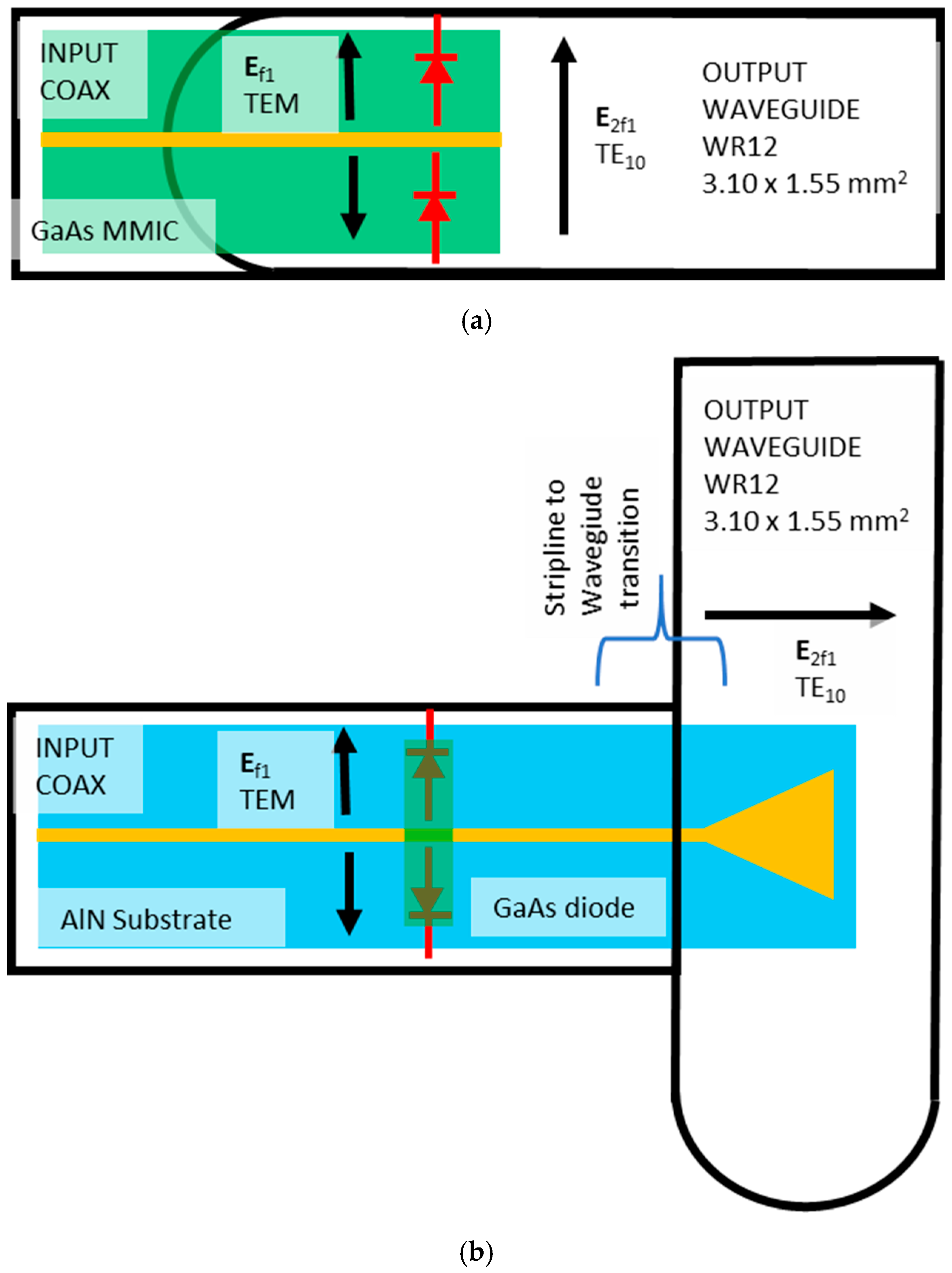
The circuit demonstrators described in this paper were fabricated using GaAs MMIC and hybrid construction technologies. Both designs aimed to provide greater than 20 mW output power between 66 GHz and 80 GHz for an input power of 250 mW, with a 3 dB bandwidth of 11 GHz. The MMIC circuit, in contrast to Porterfield’s balanced input design, places a series-connected diode pair across the output waveguide, as shown in a simplified view in
Figure 1a. Power at the fundamental frequency, f, propagates from the coaxial input to the common point of the diodes in a TEM/coaxial mode. The non-linear response of the diodes excites the output waveguide in the TE
10 mode at 2f, as desired. This simplified view omits details of the external DC bias, the integrated capacitor and that several diodes are used in series to handle the input power. This circuit topology was previously demonstrated using non-optimal diode technology with unbiased diodes [
6].
The hybrid circuit,
Figure 1b, a standard single-ended design, also has a coaxial input. This simplified view includes two diodes in an anti-series configuration from the central conductor to ground on a TEM mode transmission line. The single-ended diode output (and input) spectrum is then filtered, typically using high/low impedance transmission line filters [
7]. The output waveguide transition acts a high-pass filter and also an open circuit stub at f. Again, actual circuits will have DC bias, capacitors to ground and multiple diodes in series.
The circuit demonstrators are realized below 100 GHz, where drive power is more easily obtained and waveguide cavity machining tolerances contribute less to potential performance degradation. The technologies, both diode and circuit, could be scaled to several hundred GHz. At E-band frequencies and lower, where K connector inputs can be used, the new MMIC configuration results in considerably smaller circuits. In addition to allowing a direct comparison of the novel MMIC- and single-ended hybrid circuit topologies,
Figure 1a,b, circuit assembly, substrate materials and circuit performance are discussed and compared to other E/W-band doubler products and research papers.
2. Circuit Design and Build
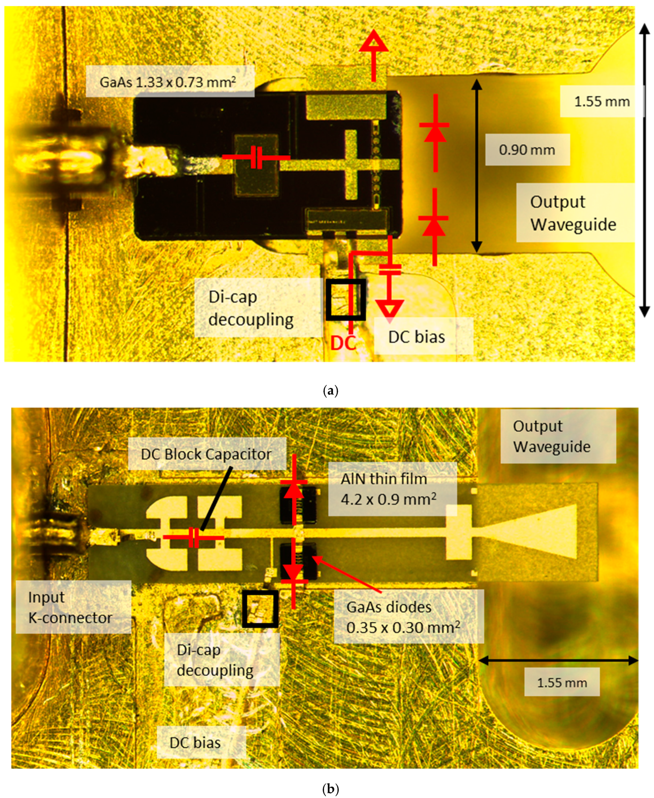
Circuit designs were performed by constructing full 3D models in Ansys HFSS for use with Keysight’s ADS harmonic balance simulator. Optimization allows anode area and the number of series-connected diodes in each arm to be chosen. For the hybrid circuit, three series-connected anodes of 48.3 (μm)2 were chosen, while the MMIC circuit used six series-connected anodes each with area 57.1 (μm)2.
Dedicated in-house processing allows metal-insulator-metal capacitors to be produced on GaAs MMIC and AlN thin film substrates. These capacitors provide either RF grounding or DC blocking. Schematic capacitor, diode and grounding configuration are overlaid on the circuit photographs in
Figure 2. Both circuits were operated in varactor mode, requiring reverse voltage bias to be applied. The series-connected MMIC diodes are biased via a beam lead connection to the top metal of the on-chip RF bypass capacitor. The MMIC RF bypass capacitor has an area of 0.4 × 0.1 mm
2, yielding 3.3 pF, and the DC blocking capacitor is 0.3 × 0.2 mm
2, yielding 5.1 pF. The hybrid circuit is biased using a short high impedance line and bond wire connection to the decoupling dicap capacitor (part D12BV101K5PX, 100 pF, 0.305 × 0.381 × 0.102 mm
3)—the same decoupling capacitor part is used in the MMIC assembly. The DC-blocking capacitor formed on the AlN substrate is 0.50 × 0.08 mm
2, yielding a capacitance of 3.3 pF. RF input power is applied in both cases via a 2.92 mm/K connector using a sliding contact to the center pin. The tab of the sliding contact is fixed to the circuits using silver-loaded epoxy.
The MMIC circuit is supported using beam leads at the circuit edge adjacent to the diodes and by a ledge under the K connector contact. The transmission line is suspended and the output waveguide extends under the diodes. In the hybrid circuit, the AlN substrate is also suspended by a lip under its edges which extends under the K connector. A cantilevered probe extends into the output waveguide.
The diode chip used in the hybrid circuit has a beam lead connection extending from the GaAs substrate and coplanar with its back surface. This enables the diode to be epoxied face-up on the substrate.
Assembling the MMIC circuit requires fewer assembly steps than the hybrid circuit—in particular, the demanding diode placement and attachment steps are eliminated. The MMIC dimensions are also considerably smaller at 1.325 × 0.725 mm2, compared to 4.2 × 0.9 mm2 for the AlN substrate. It should also be noted that MMIC technologies offer more repeatability in circuit performance due to better controlled dimensions and alignment on the circuit. Both circuits are mounted in an E-plane split block with WR-12 output waveguides (3.10 × 1.55 mm2).
3. RF Measured Results and Discussion
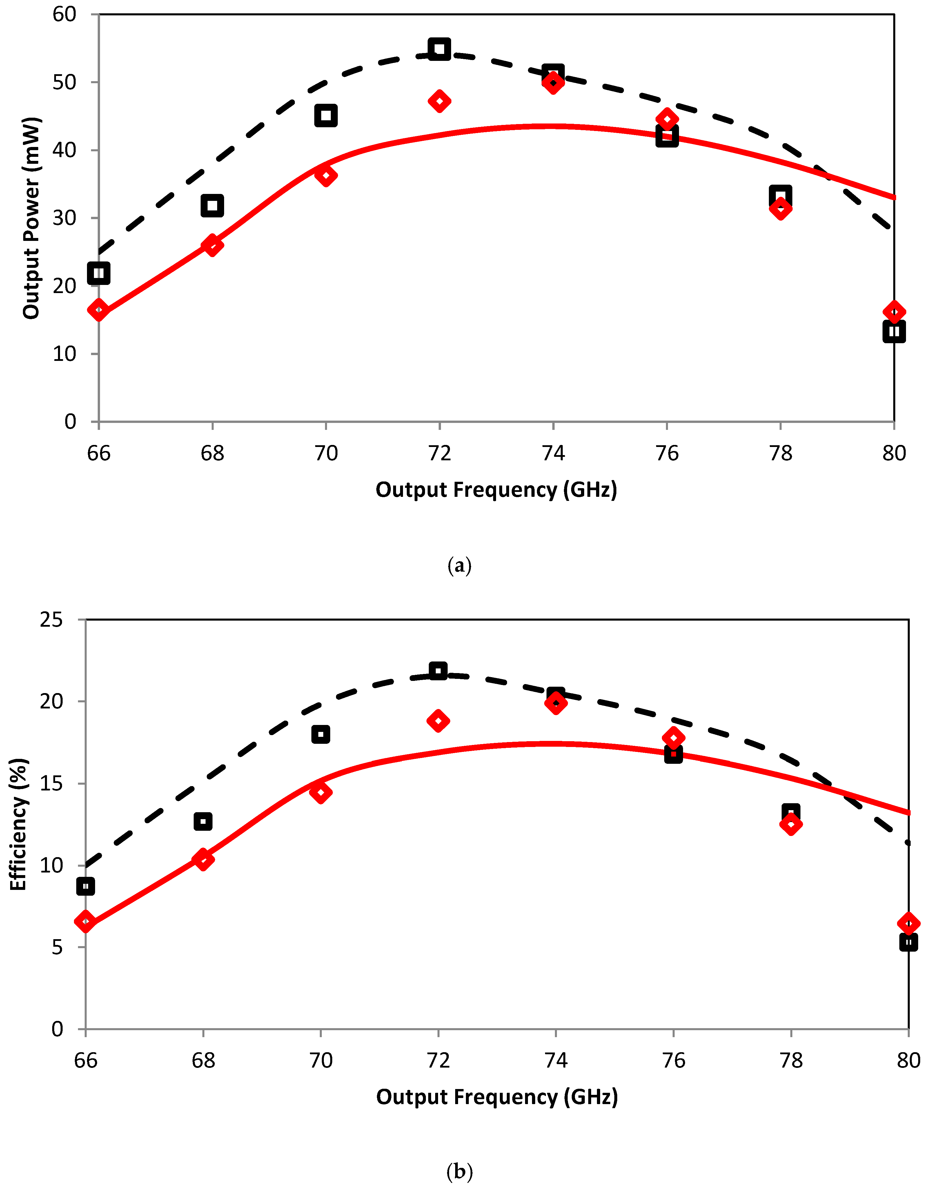
An Erickson PM4 waveguide power meter was used to record the output power from the doublers. Drive power was a continuous wave signal applied at the K connector inputs using a laboratory synthesizer via a QuinStar 20 to 45 GHz amplifier and 26.5 to 40 GHz isolator. During testing, the optimum bias conditions for peak output power and efficiency at each frequency and input power were located. For each measurement point, the process followed is: (1) a bias is applied equal to half the measured DC breakdown voltage for the device; this is the maximum bias applied during all the testing. (2) The RF signal is applied to the diode and the output power is measured. (3) Magnitude of the bias is reduced to the point where peak output power is observed.
The measured and simulated results are shown in
Figure 3 for 250 mW input power for both circuits. Measured peak output powers for both circuits are similar, yielding 50 mW and 55 mW for the hybrid and MMIC circuit, respectively. Measured 3-dB bandwidths for both circuits are 11 GHz, i.e., >15%. The circuit power response is determined by the embedding impedances presented to the diodes at input and output frequencies and also over the circuit harmonics. For these designs, peak performance was centered at the middle of the desired band.
Simulations for the MMIC correspond closely with the measurements. For the hybrid circuit, measured powers and efficiencies are more resonant than predicted by the simulation. In both cases, deviations in behavior are ascribed to imperfections in the K connector to microstrip connection transition, leading to mismatch ripples in the response.
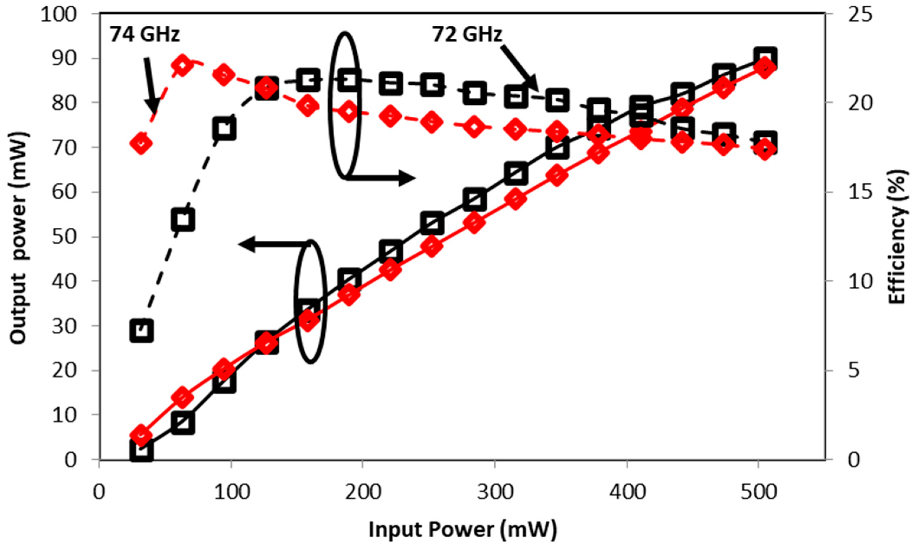
Power sweeps are plotted in
Figure 4 at the frequency corresponding to peak output power for each circuit. In each case, the efficiency initially rises to a peak then reduces more gradually as the power is increased. For both circuits, the decrease in efficiency corresponds to a measured increase in DC forward diode conduction current during test, indicating maximal voltage swing in the diodes. DC biases were limited to half the measured DC breakdown voltage during testing. It is expected that efficiency will also reduce with increasing input power due to self-heating, causing an increase in anode temperature [
8].
A comparison of the performance of a range of E/W-band doublers is given in
Table 1. Commercial datasheets and research publications are included. Although difficult to compare like-for-like directly, as different power and particularly frequency/bandwidth specifications apply, this work has shown that the power and efficiency of the described devices matches or exceeds published results over their 3 dB bandwidth.
4. Conclusions
This paper reports a demonstration of a high efficiency Schottky diode balanced frequency doubler using biased series-connected diodes in the output waveguide. The doubler was implemented using a GaAs Schottky MMIC process with integrated capacitors and beam leads. This circuit configuration is particularly well-suited for use with a coaxial input connection using the Porterfield approach [
5]. Using a simple input low-pass filter configuration makes the MMIC dimension small. Moreover, component assembly for the MMIC does not require any diode attachment process, such as gluing and bonding or flip-chip diode attachment. The large beam leads connected to the diodes and also the large area of GaAs close to the K connector, which are attached to the block, offer a low thermal resistance, making this geometry attractive for very high-power devices. Testing of these devices at higher input powers is planned. These aspects of the MMIC circuit make the technique attractive for realizing high-power doublers for use in multiplier chains for higher frequency sources. An interesting extension of this work would be to realize a high-power doubler with maximal efficiency over a complete waveguide bandwidth; for example, 60 to 90 GHz. This would require further consideration of the filtering used to achieve the diode embedding impedance and also an optimization on the number and area of the diode anodes.
Results for the MMIC doubler were compared to a more conventional single-ended hybrid doubler which uses two discrete diodes placed on a planar AlN circuit. It is noted that, in general, the use of a bespoke MMIC process, such as that described here, will be impractical and possibly less cost-effective than a hybrid circuit approach. Both MMIC and hybrid circuits yield excellent performance over the design bandwidth 67–78 GHz, with the novel MMIC design delivering 25 to 55 mW at 12 to 22% efficiency.
Author Contributions
Conceptualization, B.A. and H.S.S. in discussion with J.R.P.; design methodology and validation, J.R.P. and C.V.; investigation, C.V.; resources, B.A.; writing—original draft preparation, J.R.P.; writing—review and editing, P.G.H. All authors have read and agreed to the published version of the manuscript.
Funding
This research received no external funding
Conflicts of Interest
The authors declare no conflict of interest.
References
- Mehdi, I.; Siles, J.V.; Lee, C.; Schlecht, E. THz Diode Technology: Status, Prospects, and Applications. Proc. IEEE 2017, 105, 990–1007. [Google Scholar] [CrossRef]
- Alderman, B.; Henry, W.; Sanghera, H.; Wang, H.; Rea, S.; Ellison, B.; de Maagt, P. Schottky diode technology at Rutherford Appleton Laboratory. In Proceedings of the 2011 IEEE International Conference on Microwave Technology & Computational Electromagnetics, Beijing, China, 22–25 May 2011; pp. 4–6. [Google Scholar]
- Meng, J.; Zhang, D.; Ji, G.; Yao, C.; Jiang, C.; Liu, S. Design of a 335 GHz Frequency Multiplier Source Based on Two Schemes. Electronics 2019, 8, 948. [Google Scholar] [CrossRef] [Green Version]
- Schlecht, E.; Siles, J.V.; Lee, C.; Lin, R.; Thomas, B.; Chattopadhyay, G.; Mehdi, I. Schottky Diode Based 1.2 THz Receivers Operating at Room-Temperature and Below for Planetary Atmospheric Sounding. IEEE Trans. Terahertz Sci. Technol. 2014, 4, 661–669. [Google Scholar] [CrossRef]
- Porterfield, D.W.; Crowe, T.W.; Bradley, R.F.; Erickson, N.R. A high-power fixed-tuned millimeter-wave balanced frequency doubler. IEEE Trans. Microw. Theory Tech. 1999, 47, 419–425. [Google Scholar] [CrossRef]
- Siles, J.V.; Maestrini, A.; Alderman, B.; Davies, S.; Wang, H.; Treuttel, J.; Leclerc, E.; Narhi, T.; Goldstein, C. A Single-Waveguide In-Phase Power-Combined Frequency Doubler at 190 GHz. IEEE Microw. Wirel. Compon. Lett. 2011, 21, 332–334. [Google Scholar] [CrossRef]
- Porterfield, D.W. High-Efficiency Terahertz Frequency Triplers. In Proceedings of the 2007 IEEE/MTT-S International Microwave Symposium, Honolulu, HI, USA, 3–8 June 2007; pp. 337–340. [Google Scholar]
- Pérez-Moreno, C.G.; Grajal, J.; Viegas, C.; Liu, H.; Powell, J.; Alderman, B. Thermal analysis of high-power millimeter-wave Schottky diode frequency multipliers. In Proceedings of the 2016 Global Symp. Millimeter Waves & ESA Workshop on Millimetre-Wave Technology and Applications, Espoo, Finland, 6–8 June 2016; pp. 1–4. [Google Scholar]
- VDI WR12x2 Datasheet. Available online: https://vadiodes.com/en/wr12x2 (accessed on 10 September 2020).
- UMS CHU2277. Available online: https://www.ums-gaas.com/product/chu2277-99f/ (accessed on 10 September 2020).
- Guo, J.; Xu, J.; Cui, Y.; Qian, C. Design of a W-band single-substrate single-waveguide power-combined frequency doubler. In Proceedings of the 2012 International Conference on Microwave and Millimeter Wave Technology (ICMMT), Shenzhen, China, 5–8 May 2012; pp. 1–4. [Google Scholar]
- Hegazi, G.; Ezzeddine, A.; Phelleps, F.; McNally, P.; Pande, K.; Rice, P.; Pages, P. W-band monolithic frequency doubler using vertical GaAs varactor diode with n/sup +/ buried layer. Electron. Lett. 1991, 27, 213–214. [Google Scholar] [CrossRef]
| Publisher’s Note: MDPI stays neutral with regard to jurisdictional claims in published maps and institutional affiliations. |
© 2020 by the authors. Licensee MDPI, Basel, Switzerland. This article is an open access article distributed under the terms and conditions of the Creative Commons Attribution (CC BY) license (http://creativecommons.org/licenses/by/4.0/).

 and
and 


