Application of Polarization Coulomb Field Scattering to a Physics-Based Compact Model for AlGaN/GaN HFETs with I–V Characteristics


Abstract
:1. Introduction
2. Model
2.1. Linear Region
2.2. Saturation Region
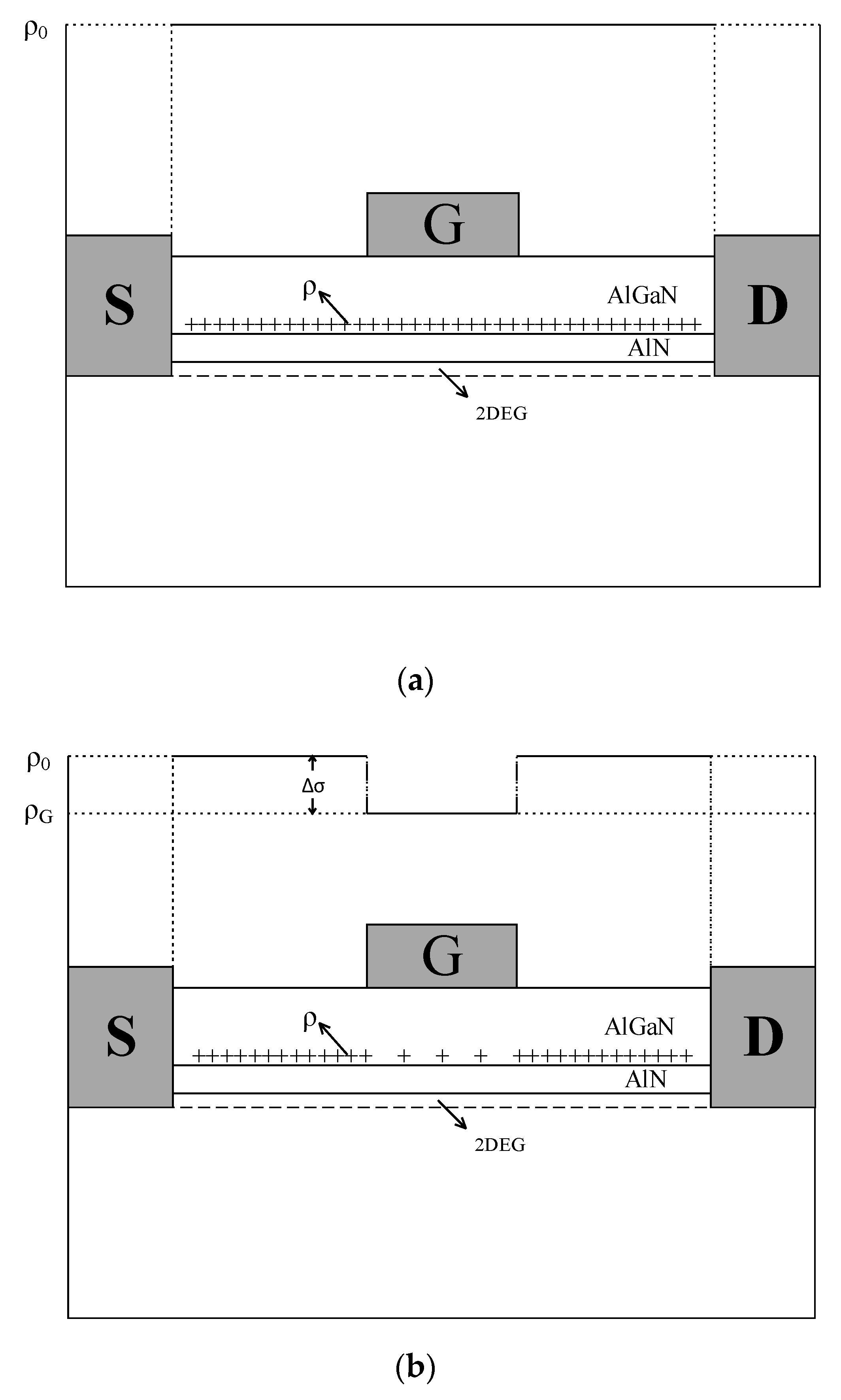
3. PCF Scattering
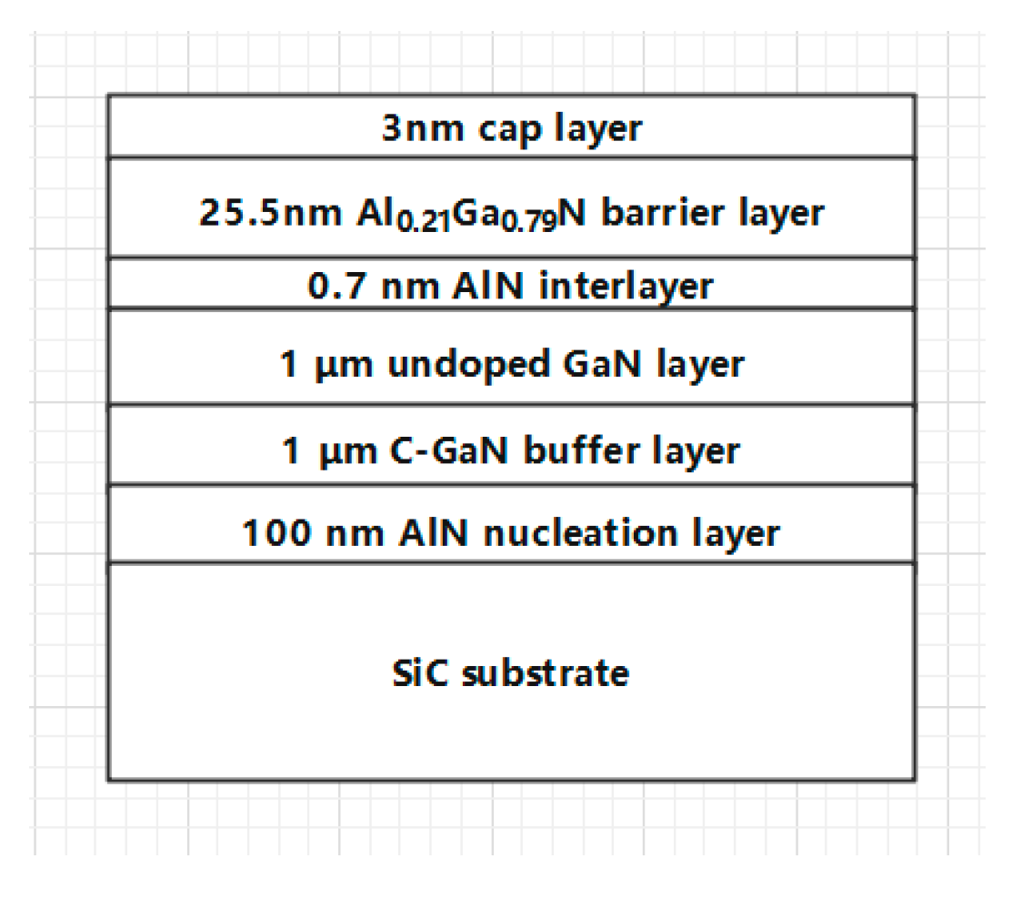
4. Experiment
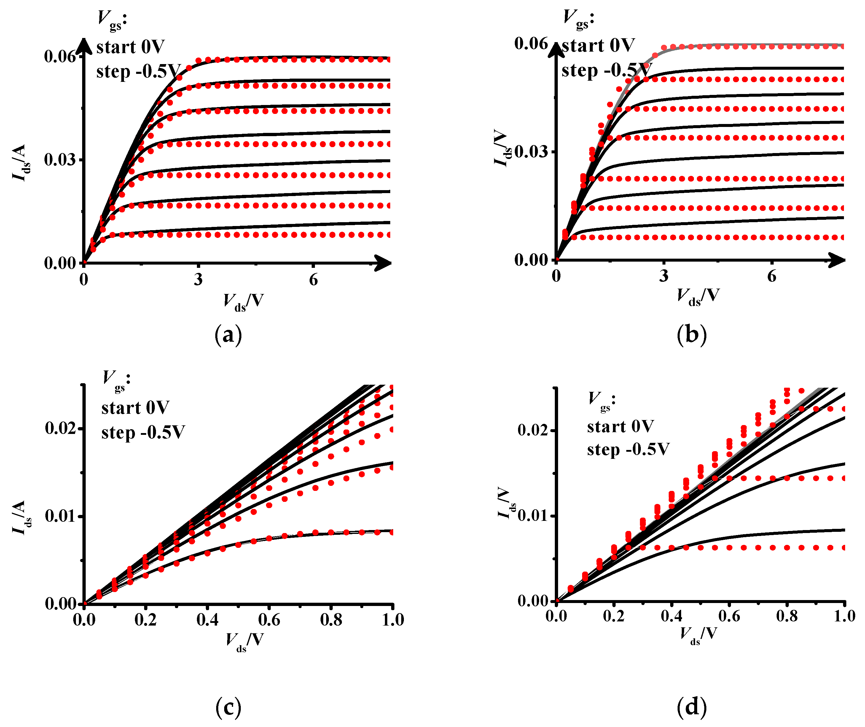
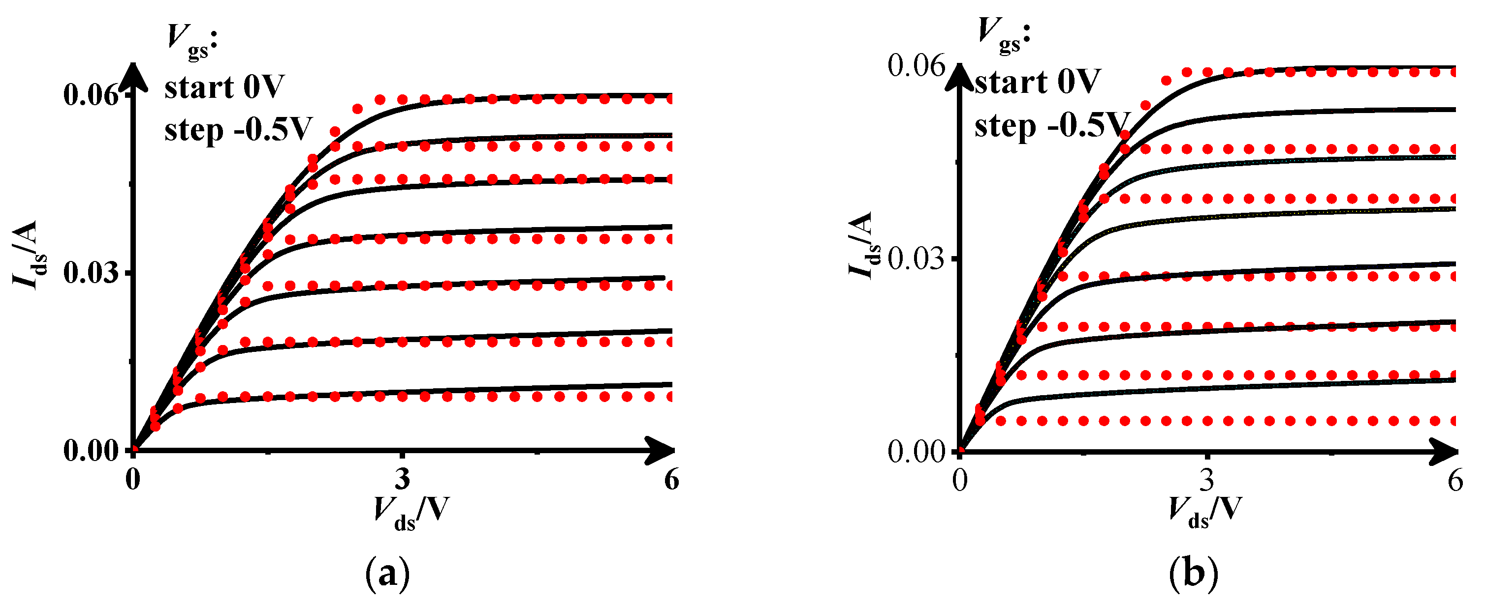
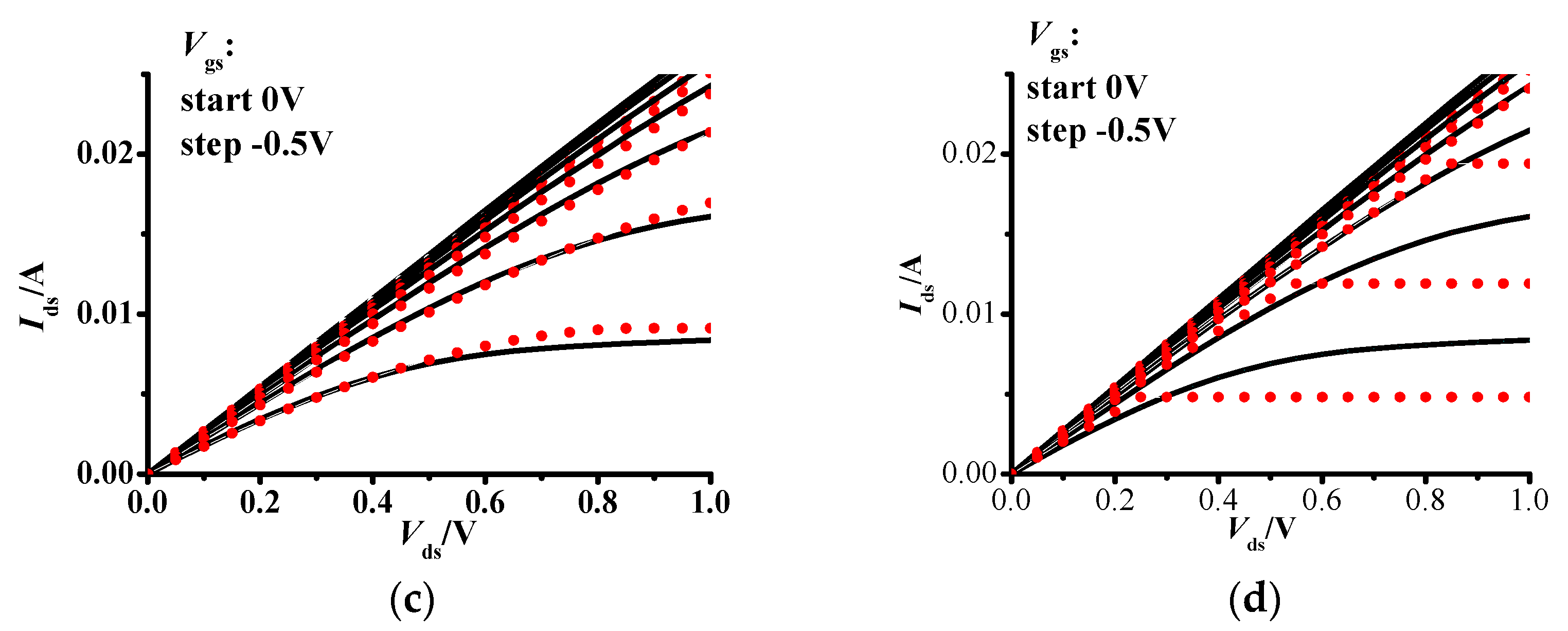
5. Comparison of Experimental and Calculated Result
6. Conclusions
Author Contributions
Funding
Conflicts of Interest
References
- Khandelwal, S.; Chauhan, Y.S.; Fjeldly, T.A.; Ghosh, S.; Pampori, A.; Mahajan, D.; Dangi, R.; Ahsan, S.A. ASM GaN: Industry Standard Model for GaN RF and Power Devices—Part 1: DC, CV, and RF Model. IEEE Trans. Electron Devices 2019, 66, 80–86. [Google Scholar] [CrossRef]
- Albahrani, S.A.; Mahajan, D.; Hodges, J.; Chauhan, Y.S.; Khandelwal, S. ASM GaN: Industry Standard Model for GaN RF and Power Devices—Part-II: Modeling of Charge Trapping. IEEE Trans. Electron Devices 2019, 66, 87–94. [Google Scholar] [CrossRef]
- Ghosh, S.; Sharma, K.; Agnihotri, S.; Chauhan, Y.S.; Iniguez, B. Modeling of temperature effects in a surface-potential based ASM-HEMT model. In Proceedings of the 2014 IEEE 2nd International Conference on Emerging Electronics (ICEE), Bengalore, India, 3–6 December 2014; pp. 1–4. [Google Scholar]
- Khandelwal, S.; Chauhan, Y.S.; Hodges, J.; Albahrani, S.A. Non-Linear RF Modeling of GaN HEMTs with Industry Standard ASM GaN Model (Invited). In Proceedings of the 2018 IEEE BiCMOS and Compound Semiconductor Integrated Circuits and Technology Symposium (BCICTS), San Diego, CA, USA, 15–17 October 2018; pp. 93–97. [Google Scholar]
- Turin, V.O. A modified transferred-electron high-field mobility model for GaN devices simulation. Solid-State Electron. 2005, 49, 1678–1682. [Google Scholar] [CrossRef]
- Jazaeri, F.; Sallese, J. Charge-Based EPFL HEMT Model. IEEE Trans. Electron Devices 2019, 66, 1218–1229. [Google Scholar] [CrossRef]
- Moon, B.; Byun, Y.H.; Lee, K.; Shur, M. New continuous heterostructure field-effect-transistor model and unified parameter extraction technique. IEEE Trans. Electron Devices 1990, 37, 908–919. [Google Scholar] [CrossRef]
- Avolio, G.; Schreurs, D.M.M.; Raffo, A.; Crupi, G.; Vannini, G.; Nauwelaers, B. Waveforms-Only Based Nonlinear De-Embedding in Active Devices. IEEE Microw. Wirel. Compon. Lett. 2012, 22, 215–217. [Google Scholar] [CrossRef]
- Avolio, G.; Schreurs, D.; Raffo, A.; Crupi, G.; Angelov, I.; Vannini, G.; Nauwelaer, B. Identification technique of FET model based on vector nonlinear measurements. Electron. Lett. 2011, 47, 1323–1324. [Google Scholar] [CrossRef]
- Lime, F.; Iniguez, B.; Moldovan, O. A Quasi-Two-Dimensional Compact Drain–Current Model for Undoped Symmetric Double-Gate MOSFETs Including Short-Channel Effects. IEEE Trans. Electron Devices 2008, 55, 1441–1448. [Google Scholar] [CrossRef]
- Yigletu, F.M.; Inigue, B.; Khandelwal, S.; Fjeldly, T.A. A compact charge-based physical model for AlGaN/GaN HEMTs. In Proceedings of the IEEE Radio and Wireless Symposium, RWS, Austin, TX, USA, 20–23 January 2013; pp. 274–276. [Google Scholar]
- Yin, H.; Hou, D.; Bilbro, G.L.; Trew, R.J. Harmonic balance simulation of a new physics based model of the AlGaN/GaN HFET. In Proceedings of the IEEE MTT-S International Microwave Symposium Digest, Atlanta, GA, USA, 15–20 June 2008; pp. 1425–1428. [Google Scholar]
- Luan, C.; Lin, Z.; Lv, Y.; Zhao, J.; Wang, Y.; Chen, H.; Wang, Z. Theoretical model of the polarization Coulomb field scattering in strained AlGaN/AlN/GaN heterostructure field-effect transistors. J. Appl. Phys. 2014, 116, 044507. [Google Scholar] [CrossRef]
- Lv, Y.; Lin, Z.; Zhan, Y.; Meng, L.; Luan, C.; Cao, Z.; Chen, H.; Wang, Z. Polarization Coulomb field scattering in AlGaN/AlN/GaN heterostructure field-effect transistors. Appl. Phys. Lett. 2011, 98, 123512. [Google Scholar] [CrossRef]
- Cui, P.; Mo, J.; Fu, C.; Lv, Y.; Lv, H.; Chen, A.; Luan, C.; Zhou, Y.; Gang, D.; Lin, Z. Effect of Different Gate Lengths on Polarization Coulomb Field Scattering Potential in AlGaN/GaN Heterostructure Field-Effect Transistors. Sci. Rep. 2018, 8, 9036. [Google Scholar] [CrossRef] [PubMed]
- Cui, P.; Lv, Y.; Lv, H.; Chen, A.; Lin, Z. Improved Linearity with Polarization Coulomb Field Scattering in AlGaN/GaN Heterostructure Field-Effect Transistors. Sci. Rep. 2018, 8, 983. [Google Scholar] [CrossRef] [PubMed] [Green Version]
- Cui, P.; Lv, H.; Lin, W.; Lin, Z.; Chen, A.; Yang, M.; Liu, Y.; Chen, F.; Lv, Y.; Luan, C. Influence of Different Gate Biases and Gate Lengths on Parasitic Source Access Resistance in AlGaN/GaN Heterostructure FETs. IEEE Trans. Electron Devices 2017, 64, 908–919. [Google Scholar] [CrossRef]
- Cui, P.; Lv, Y.; Lin, Z.; Fu, C.; Liu, Y. Effect of polarization Coulomb field scattering on device linearity in AlGaN/GaN heterostructure field-effect transistors. J. Appl. Phys. 2017, 122, 124508. [Google Scholar] [CrossRef]
- Yang, M.; Lin, Z.; Zhao, J.; Cui, P.; Fu, C.; Lv, Y.; Feng, Z. Effect of polarization Coulomb field scattering on parasitic source access resistance and extrinsic transconductance in AlGaN/GaN heterostructure FETs. IEEE Trans. Electron Devices 2016, 63, 1471–1477. [Google Scholar] [CrossRef]
- Gurusinghe, M.N.; Davidsson, S.K.; Andersson, T.G. Two-dimensional electron mobility limitation mechanisms in AlxGa1-xN/GaN heterostructures. Phys. Rev. B 2005, 72, 045316. [Google Scholar] [CrossRef]
- Jiang, G.; Lv, Y.; Lin, Z.; Yang, Y.; Yang, L.; Guo, S.; Zhou, Y. Polarization Coulomb field scattering with the electron systems in AlGaN/GaN heterostructure field-effect transistors. AIP Adv. 2020, 10, 075212. [Google Scholar] [CrossRef]


| Symbol | Meaning | Quantity | 0.25 μm Gate Length Device | 0.5 μm Gate Length Device |
|---|---|---|---|---|
| Ci | Gate-to-channel capacitance | F/m2 | 3.45 | 3.45 |
| vsat | Electron saturation velocity | cm/s | 4.02 | 6.5 |
| Fs | Characteristic field of the velocity saturation | V/m | 2.05 | 3.72 |
| Vt | Threshold voltage | V | −3.9 | −3.9 |
| n2-D | Two-dimensional electron density in zero bias | m−2 | 8.4 | 8.4 |
| Gate Bias/V | RS(Including Ohmic Resistance)/Ω | RD(Including Ohmic Resistance)/Ω | |
|---|---|---|---|
| 0 | 1720 | 10.28 | 24.41 |
| −0.5 | 1683 | 10.22 | 24.34 |
| −1 | 1611 | 10.25 | 24.38 |
| −1.5 | 1553 | 10.18 | 24.30 |
| −2 | 1418 | 10.17 | 24.29 |
| −2.5 | 1220 | 10.18 | 24.30 |
| −3 | 889 | 10.69 | 24.86 |
| Gate Bias/V | RS(Including Ohmic Resistance)/Ω | RD(Including Ohmic Resistance)/Ω | |
|---|---|---|---|
| 0 | 1748 | 10.02 | 24.13 |
| −0.5 | 1721 | 10.13 | 24.21 |
| −1 | 1667 | 10.08 | 24.18 |
| −1.5 | 1607 | 10.12 | 24.21 |
| −2 | 1476 | 10.20 | 24.27 |
| −2.5 | 1287 | 10.33 | 24.38 |
| −3 | 1065 | 11.60 | 25.46 |
Publisher’s Note: MDPI stays neutral with regard to jurisdictional claims in published maps and institutional affiliations. |
© 2020 by the authors. Licensee MDPI, Basel, Switzerland. This article is an open access article distributed under the terms and conditions of the Creative Commons Attribution (CC BY) license (http://creativecommons.org/licenses/by/4.0/).
Share and Cite
Yang, Y.; Lv, Y.; Lin, Z.; Jiang, G.; Liu, Y. Application of Polarization Coulomb Field Scattering to a Physics-Based Compact Model for AlGaN/GaN HFETs with I–V Characteristics. Electronics 2020, 9, 1719. https://doi.org/10.3390/electronics9101719
Yang Y, Lv Y, Lin Z, Jiang G, Liu Y. Application of Polarization Coulomb Field Scattering to a Physics-Based Compact Model for AlGaN/GaN HFETs with I–V Characteristics. Electronics. 2020; 9(10):1719. https://doi.org/10.3390/electronics9101719
Chicago/Turabian StyleYang, Yongxiong, Yuanjie Lv, Zhaojun Lin, Guangyuan Jiang, and Yang Liu. 2020. "Application of Polarization Coulomb Field Scattering to a Physics-Based Compact Model for AlGaN/GaN HFETs with I–V Characteristics" Electronics 9, no. 10: 1719. https://doi.org/10.3390/electronics9101719