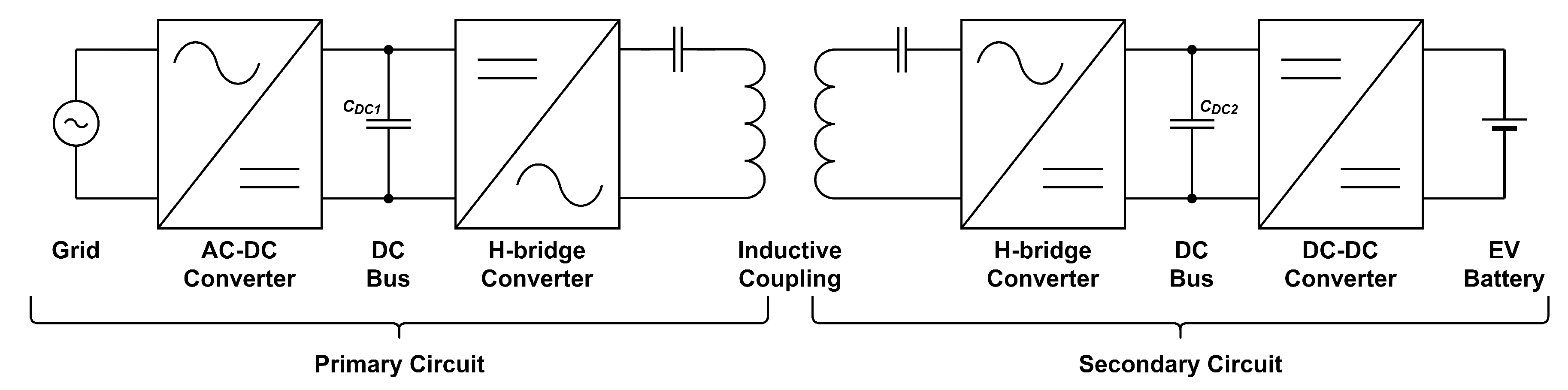
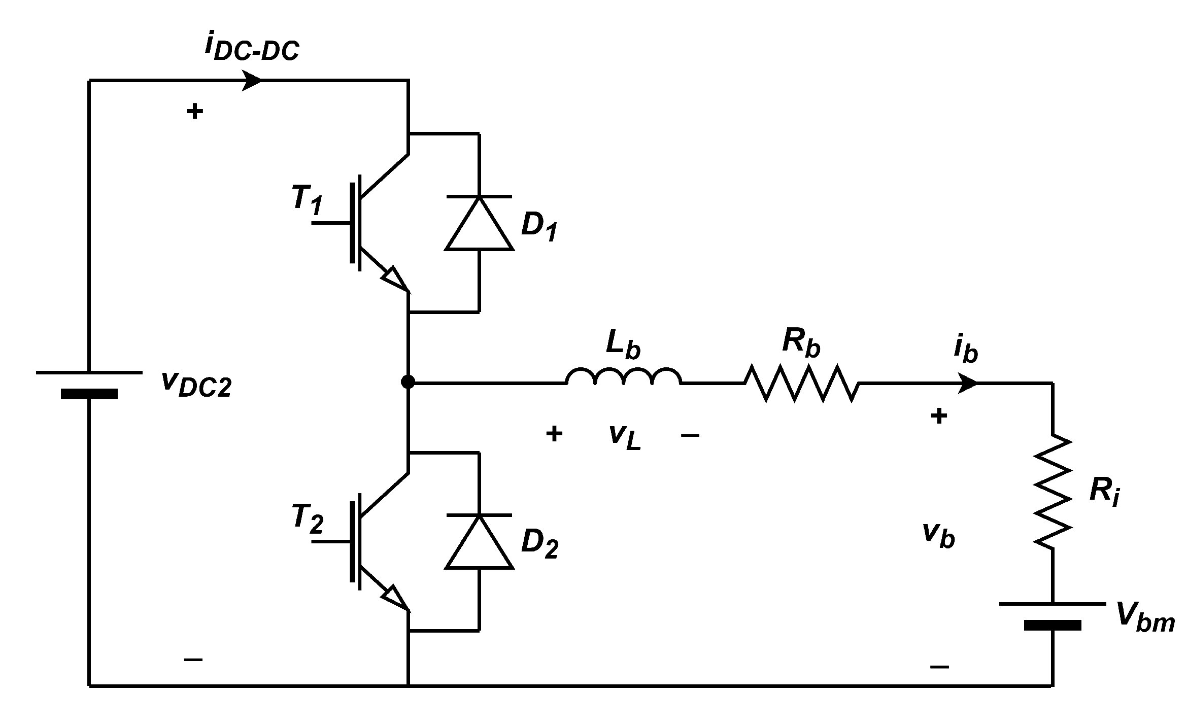
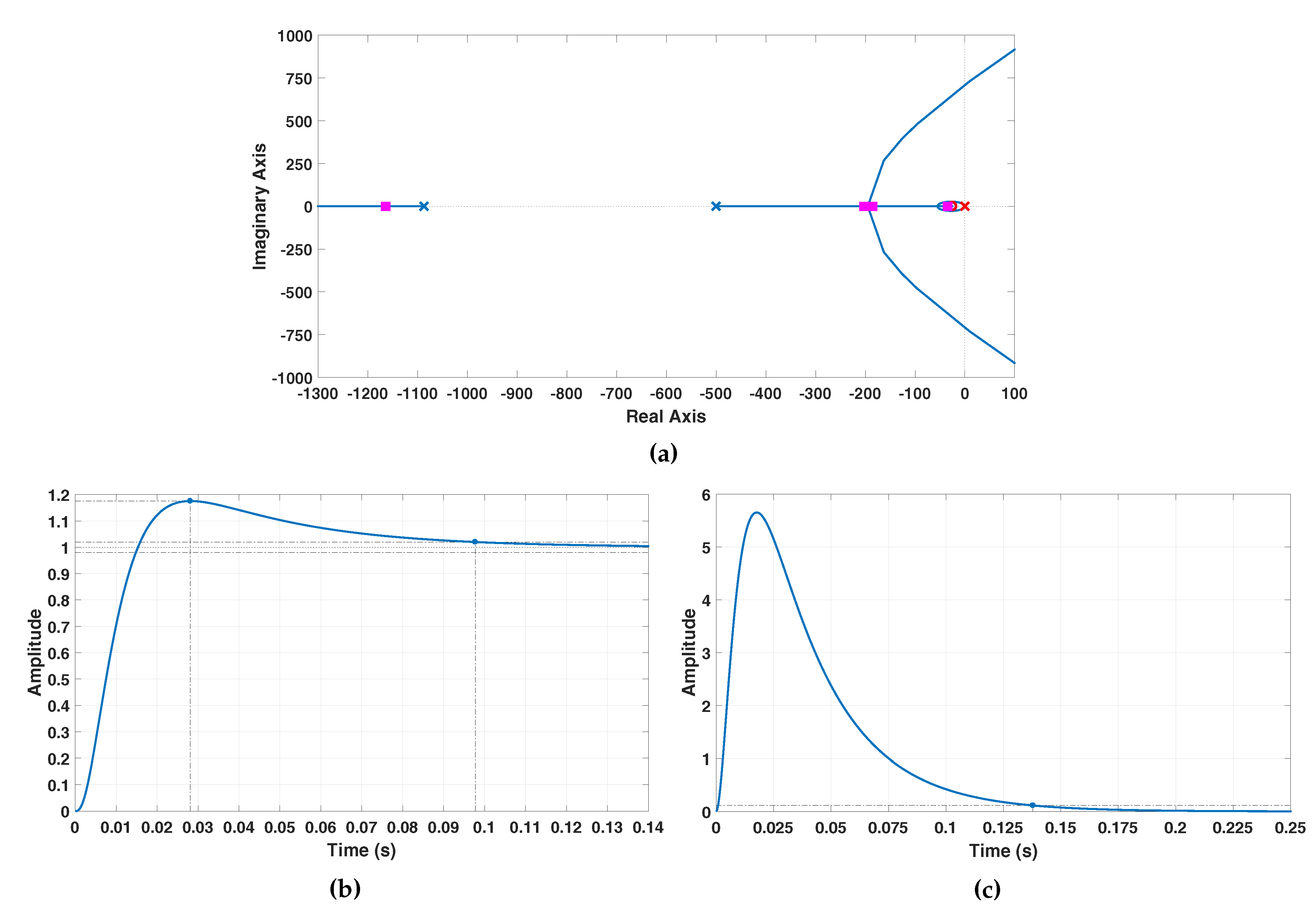
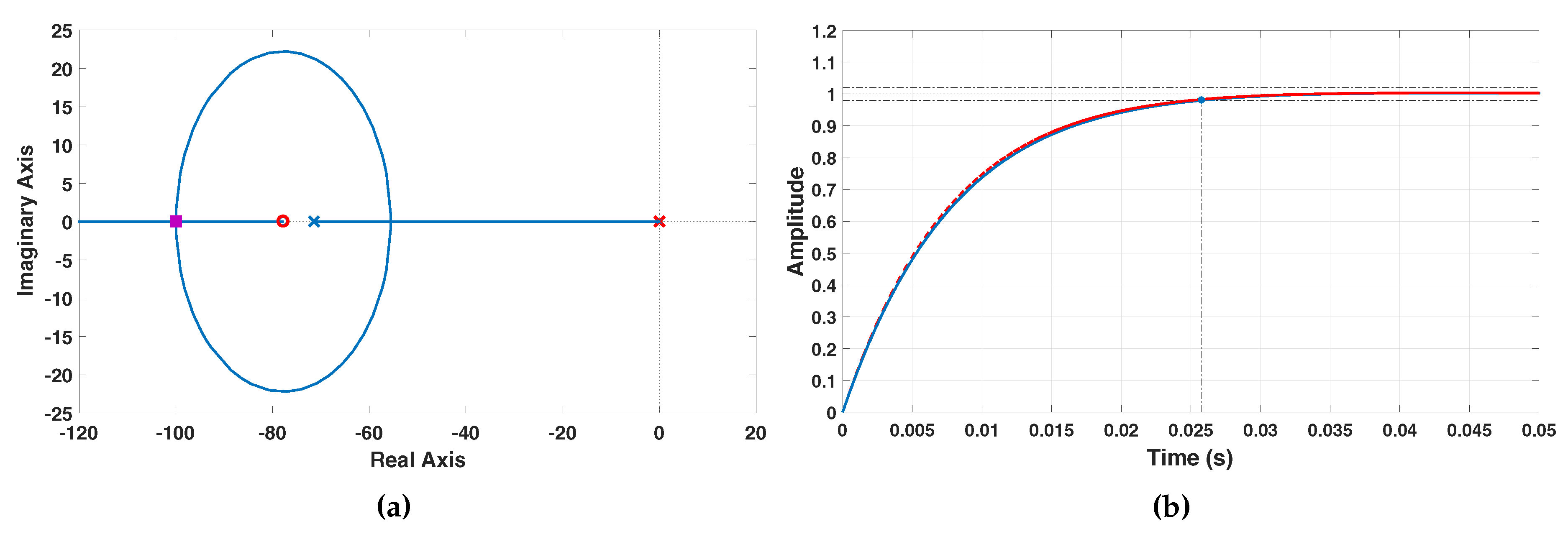
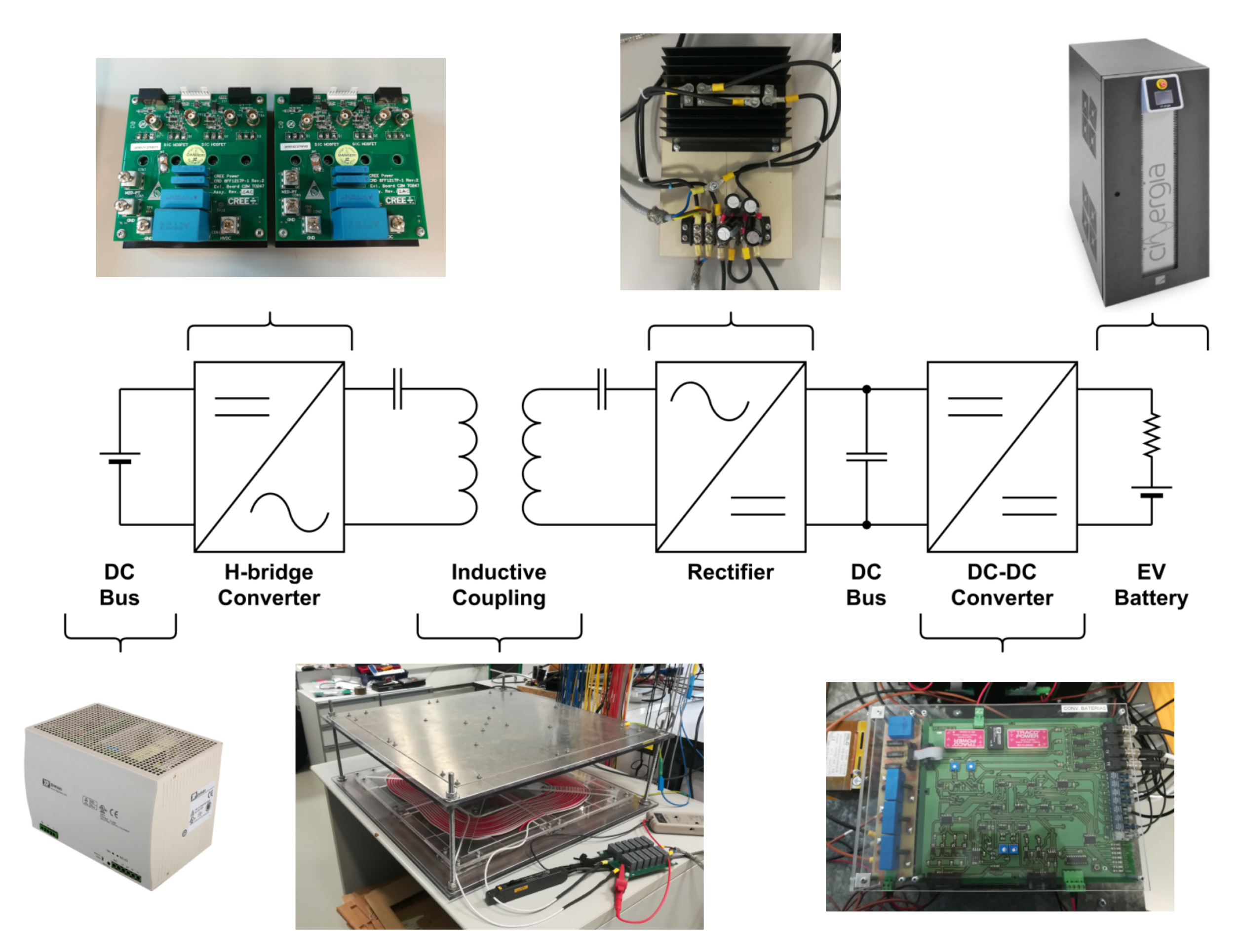
Article

Control Scheme of a Bidirectional Inductive Power Transfer System for Electric Vehicles Integrated into the Grid

by
Emilio J. Molina-Martínez
1,
Pedro Roncero-Sánchez
1,*,
Francisco Javier López-Alcolea
1,
Javier Vázquez
1 and
Alfonso Parreño Torres
2
1
Institute of Energy Research and Industrial Applications, University of Castilla-La Mancha, Campus Universitario S/N, 13071 Ciudad Real, Spain
2
Institute of Industrial Development, Castilla-La Mancha Science and Technology Park, Paseo de la Innovación 1, 02006 Albacete, Spain
*
Author to whom correspondence should be addressed.
Electronics 2020, 9(10), 1724; https://doi.org/10.3390/electronics9101724
Submission received: 19 August 2020 / Revised: 1 October 2020 / Accepted: 8 October 2020 / Published: 19 October 2020
(This article belongs to the Special Issue Advances in Power Electronics for Transportation Electrification)

Abstract

:
Inductive power transfer (IPT) systems have become a very effective technology when charging the batteries of electric vehicles (EVs), with numerous research works devoted to this field in recent years. In the battery charging process, the EV consumes energy from the grid, and this concept is called Grid-to-Vehicle (G2V). Nevertheless, the EV can also be used to inject part of the energy stored in the battery into the grid, according to the so-called Vehicle-to-Grid (V2G) scheme. This bidirectional feature can be applied to a better development of distributed generation systems, thus improving the integration of EVs into the grid (including IPT-powered EVs). Over the past few years, some works have begun to pay attention to bidirectional IPT systems applied to EVs, focusing on aspects such as the compensation topology, the design of the magnetic coupler or the power electronic configuration. Nevertheless, the design of the control system has not been extensively studied. This paper is focused on the design of a control system applied to a bidirectional IPT charger, which can operate in both the G2V and V2G modes. The procedure design of the control system is thoroughly explained and classical control techniques are applied to tailor the control scheme. One of the advantages of the proposed control scheme is the robustness when there is a mismatch between the coupling factor used in the model and the real value. Moreover, the control system can be used to limit the peak value of the primary side current when this value increases, thus protecting the IPT system. Simulation results obtained with PSCADTM/EMTDCTM show the good performance of the overall system when working in both G2V and V2G modes, while experimental results validate the control system behavior in the G2V mode.

1. Introduction

Recent scientific research reports that the current global warming situation is taking place faster than any other change that has occurred in the last 2000 years [1,2]. Owing to this fact, a social concern has increased in the last few decades, and several actions have been taken into account in order to slow down climate change. One of the clearest examples is a constant growth in the use of renewable energy sources, or clean energies. Nevertheless, the continuous increase in the greenhouse gases, particularly CO2 [3,4], and, hence, in the global warming, renders the applied measures insufficient. Specifically, according to the annual report presented by the European Union in October 2019 with regard to the estimated inventory of greenhouse gases in 2018, energy-related emissions were reduced in all sectors except the transport sector, where emissions increased for the fifth year in a row, meaning an increase of 4.8 Mt CO2 eq. with regard to the total emissions of the previous year [5].
For that reason, a change of paradigm is needed in which the energy transition will play a key role. This transition should allow a dramatic reduction in the CO2 emissions in order to obtain 100% of the energy from renewable sources. In order to achieve this goal, among other actions, a transition from internal-combustion engine vehicles to electric vehicles (EVs) should be implemented.
The widespread adoption of EVs will allow the emissions caused by the transport sector to be reduced. Moreover, a better development of the distributed generation system will be achieved with the integration of the vehicle-to-grid (V2G) operation mode on a large scale. Nowadays, conductive charging is the usual method employed by EVs to recharge their batteries. However, in the last decade, the wireless power transfer (WPT) technology has experienced a great development and can be regarded as a contactless alternative approach for EV battery charging [6]. In accordance with [7], the efficiency of conductive chargers is usually higher than that of contactless technology owing to a lower number of power conversion stages. Nevertheless, some WPT systems are able to reach efficiencies close to 96%, as explained in [8]. Furthermore, the absence of mechanical connectors and the lack of electrical contact between the EV and the charging station in WPT systems allow the operation in moist environments, improving the safety for the user [9,10]. In addition, a disadvantage of conductive chargers is that the wires used for connecting the car to the grid are prone to vandalism [11]. On the other hand, WPT systems are more difficult to design than conductive chargers as a trade-off between the coil size and the transmission efficiency should exist. From the point of view of the control system, conductive chargers are regulated by simpler control structures as they contain less stages than WPT systems. A comprehensive comparison of both technologies can be found in [7].
WPT systems are composed of a transmitter and a receiver that are coupled by means of different types of fields, allowing the energy transfer between both elements. The WPT systems are classified in accordance with the nature of the coupling field, and they are suitable for different applications. Two technologies can be used in the charging process of EVs: If the WPT systems rely on an electric field, they are called capacitive power transfer (CPT) systems, while those that employ a magnetic field for the coupling are called inductive power transfer (IPT) systems. Currently, IPT schemes provide a superior performance compared to CPT systems in terms of efficiency, power density, and safety protection against field emissions [12]. For these reasons, IPT systems are normally used for charging EVs.
Two magnetically coupled coils are the core of any IPT system. As they are loosely coupled systems, capacitors with which to compensate the self-inductance of the coils are used in order to not only increase the transferred power and the efficiency, but also to reduce the grid current when the system operates at the resonance frequency [13]. Although there are several compensation topologies, the basic topologies only employ a compensation capacitor on the primary winding side and another one on the secondary winding side. The connection of these capacitors with the corresponding coils can be either in series (S) or in parallel (P), yielding the following four compensation schemes: SS, SP, PP, and PS, where the first and the second letters stand for the connection of the capacitor at the primary and the secondary windings.
These four basic compensation configurations exhibit advantages and drawbacks [14]. Nevertheless, the SS topology is one of the favorites to be used in IPT systems for charging EVs, since the resonance frequency is independent of the coupling factor and the load, which allows the IPT system to be operated at a constant frequency [15]. Furthermore, the SS topology is suitable for bidirectional power transfer applications owing to its symmetrical structure. Another advantage is a higher efficiency for a wide range of load currents [16]. On the other hand, the SS topology resembles a voltage source when the current through the primary circuit is kept constant [14], whereas it has a current-source behavior if the voltage on the primary side is maintained constant [17]. In this last case, an additional control scheme or protection circuit should be used to regulate the current through the primary winding in order to prevent overcurrents caused by the operation with low values of the secondary current, e.g., when the battery of the EV is charged in the constant–voltage mode [18].
In order to overcome the drawbacks of the SS topology, more complex compensation schemes have been proposed in the literature [19]. The LCL topology is one of these examples, which is obtained by inserting additional coils in series on both sides of a PP compensation topology [20]. Another topology can be found in [21], where a CLC resonant tank is developed to reduce the voltage stress across the power semiconductors. In [22], an LCC-parallel compensation scheme is used, as it offers more efficiency than other topologies. Nonetheless, as these topologies are more complex, their size and the cost of the electronics increases with regard to the basic compensation schemes. For this reason, the chosen topology for this paper is the SS compensation scheme.
Different works have previously dealt with the design of the control scheme of an IPT system for charging EVs. In [23], a control scheme for an IPT system with an LCCL network on the secondary side is designed. A DC–DC converter connected to the battery is controlled in order to manage the battery charging. The LCCL compensation topology generates a constant output voltage on the secondary side, which is a desirable feature for controlling the DC–DC converter. Nevertheless, this goal can also be achieved by using a simpler compensation scheme with an appropriate control scheme. The system proposed in [23] is able to operate with a wide variation of the coupling coefficient. On the other hand, a control scheme based on the Ziegler–Nichols method is proposed in [24]: as this method is a heuristic technique, the resulting controller is easily obtained, but it should be optimized in order to improve the time response of the variables to be controlled. Its control scheme is tailored for a constant value of the coupling factor, but the performance of the controller is not tested when the coupling factor undergoes variations. Moreover, in [25], a control system for a contactless power transfer system is presented, although the design procedure is not explained. Another control scheme for the battery charging of an EV by means of an IPT system is found in [26]. It employs a hybrid compensation topology to select the charging mode of the battery: constant current or constant voltage. The lack of a suitable control system makes this solution complicated compared to other approaches that only use a basic compensation scheme.
This paper is focused on the design of a control system for a bidirectional IPT system that uses an SS compensation, in order to establish a bidirectional power flow between the grid and the battery of the EV. To achieve this goal, the control system regulates the DC voltages on both sides of the IPT system, thus avoiding overvoltages. Unlike other previous references that dealt with the control design for IPT applications, comprehensive information about the design criteria and the design methodology is provided in this work. Moreover, the design procedure can be applied to other compensation topologies. Furthermore, the dynamic performance obtained with the control system is analyzed when there is a mismatch in the coupling factor. The control system is also able to reduce the current through the primary side by reducing the voltage on the secondary side, avoiding one of the main drawbacks of the SS-compensated systems, which are prone to exhibit large currents through the primary side when there are misalignments. Another important feature is that the control system is tailored when the load is a battery, unlike other works that design the control scheme considering the load as an equivalent resistance [25].
The paper is organized as follows: the description of the bidirectional IPT system is presented in Section 2. Section 3 deals with the management of both operation modes of the IPT system, i.e., the grid-to-vehicle (G2V) and the V2G modes, whereas the control topology and the control design procedure are thoroughly explained in Section 4. Simulation results obtained by using PSCADTM/EMTDCTM are presented in Section 5, while some preliminary experimental results are obtained in Section 6. The main conclusions are provided in Section 7.

2. Description of the Proposed IPT System

Figure 1 shows the proposed configuration of the IPT system featuring an SS compensation topology. The key elements are two weakly coupled windings, known as primary and secondary coils, along with various power electronic converters that are devoted to control the bidirectional energy flow between the grid and the EV. The main difference between this scheme and a unidirectional IPT system is that all the power converters are bidirectional, and they can, therefore, operate either as inverters or rectifiers. Furthermore, in this work, a DC–DC converter is proposed to control the current through the battery: unlike other works that connect the battery directly to the output of the H-bridge converter on the secondary side [27], the use of a DC–DC converter is adopted, as this solution adapts the voltage levels of the H-bridge converter and the battery, offering, thus, an additional degree of freedom and eliminating from the control platform extra communication devices used to transmit the information of the power flow that exists between both sides of the IPT system [28].
The converter associated with the grid is an AC–DC converter with a topology based on a three-phase voltage-source inverter (VSI), and is connected to the grid by means of an inductive filter, as shown in Figure 2. The goal of this converter is to maintain the DC input voltage of the H-bridge converter v D C 1 constant, while compensating the reactive power exchanged with the grid. The control design of this converter has been omitted for the sake of simplicity, since previous research works have already dealt with this converter [29].
The compensated magnetic coupler, along with two H-bridge converters, are shown in Figure 3: an SS compensation topology has been used in this work for the reasons explained in Section 1. The capacitors C 1 and C 2 are designed in order to compensate the winding self-inductances L 1 and L 2 , respectively, at the operating frequency of the system, achieving, thus, maximum power transfer. The capacitances are, therefore, obtained as:
C 1 = 1 ω r 2 L 1
C 2 = 1 ω r 2 L 2
where ω r is the operating frequency, i.e., the resonance frequency, and the mutual inductance between the two coils can be calculated as [30]:
M = k L 1 L 2
where k is the coupling factor.
The analysis of the IPT system is carried out by using the approach based on the T-model of a transformer owing to its simplicity [13], as shown in Figure 4. In this model, R 1 and R 2 are the stray resistances of the primary and the secondary coils, respectively, whereas L 1 e and L 2 e are the leakage inductances of the primary winding and the secondary winding, respectively, and are obtained as:
L 1 e = ( 1 k ) L 1
L 2 e = ( 1 k ) L 2
Furthermore, the H-bridge converter on the primary side is operated by the phase-shift control technique in order to regulate the DC voltage v D C 2 on the secondary side, i.e., the input voltage of the DC–DC converter shown in Figure 1. Note that the phase-shift control action makes the SS compensation topology behave as a voltage source [14]. Owing to the phase-shift control, the H-bridge converter output voltage at the primary-side, v 1 , contains only odd harmonics whose amplitudes can be obtained as [31]:
V ^ 1 h = 4 v D C 1 π h cos ( h α )
where h is the harmonic order and α is the phase-shift angle.
The H-bridge converter on the secondary side operates in square-waveform mode, which implies that the DC value of the converter output current; i 0 , can be obtained as:
I 0 = 2 π I ^ 2
where I 0 is the DC value of the current i 0 and I ^ 2 is the peak amplitude of the current that flows through the secondary coil, as shown in Figure 3, assuming that this current will be an almost sinusoidal waveform owing to the high values of the leakage inductances [15].
In the phasor domain, the impedances Z 1 and Z 2 of both the primary and the secondary coils plus the series compensation capacitors are obtained as:
Z 1 = j ω L 1 + 1 j ω C 1 + R 1
Z 2 = j ω L 2 + 1 j ω C 2 + R 2
Furthermore, the currents that flow through the two windings can be obtained as:
I ¯ 1 ( j ω ) = Z 2 Z 1 Z 2 + ω 2 M 2 V ¯ 1 ( j ω ) j ω M Z 1 Z 2 + ω 2 M 2 V ¯ 2 ( j ω )
I ¯ 2 ( j ω ) = Z 1 Z 1 Z 2 + ω 2 M 2 V ¯ 2 ( j ω ) + j ω M Z 1 Z 2 + ω 2 M 2 V ¯ 1 ( j ω )
As the H-bridge converters operate at the resonance frequency ω r , Equations (8) and (9) become Z 1 = R 1 and Z 2 = R 2 , respectively, in steady-state. Moreover, as the stray resistances have negligible values, the phasor currents (10) and (11) can be simplified as:
I ¯ 1 ( j ω r ) V ¯ 2 ( j ω r ) j ω r M
I ¯ 2 ( j ω r ) V ¯ 1 ( j ω r ) j ω r M
As explained before, the input voltage of the DC–DC converter v D C 2 is kept constant by controlling the phase-shift angle α of the output voltage of the H-bridge converter on the primary side. In accordance with [28], the IPT system with SS compensation can, therefore, be approximated by a constant voltage source. The topology of this DC–DC converter is a bidirectional step-down converter and must deal with the control of the current injected/extracted into/from the battery of the EV. Figure 5 shows the scheme of the DC–DC converter with the constant voltage source v D C 2 , where L b and R b are the inductance and the resistance, respectively, of the filter employed to connect the converter to the battery, i b is the current that flows through the battery and v b is the battery voltage. The model of the battery used in this work employs a voltage source V b m , which represents the electromotive force, and an internal series resistance R i [32].
Assuming that the DC–DC converter operates in the continuous conduction mode (CCM) that only one of the switches can be turned on, and using the state-space averaging technique, the state-space equation of the DC–DC converter when the transistor T 1 is switched on is:
d i b ON d t = R b + R i L b i b ON V b m L b + v D C 2 L b
whereas the equation of the DC–DC converter obtained when the transistor T 1 is switched off is:
d i b OFF d t = R b + R i L b i b OFF V b m L b
Let d be the duty ratio of the switch T 1 . An average model can be obtained if the current i b is assumed to be constant over a switching period, Equation (14) is multiplied by d and Equation (15) is multiplied by ( 1 d ) :
d i b d t = R b + R i L b i b V b m L b + v D C 2 L b d
where i b is the average value of the current i b . Moreover, the resulting average system (16) is also a linear system whose steady-state operating point can be calculated by setting the time derivative of the average value i b to zero, yielding:
V b m 0 = v D C 2 0 D 0 R b + R i I b 0
where the subscript 0 refers to the variable values at the operating point. From Figure 5, the battery voltage can be calculated as v b = V b m + R i i b and Equation (17) can, therefore, be written as:
V b 0 = v D C 2 0 D 0 R b I b 0

3. Management of the Charge and Discharge of the Battery

In accordance with Equation (12), the voltage phasor V ¯ 2 has a phase lead of 90° with regard to the current phasor I ¯ 1 . Similarly, the current phasor I ¯ 2 has also a 90° phase lead with regard to the voltage phasor V ¯ 1 , according to (13). These phase leads are plotted in Figure 6:
In order to achieve maximum power transfer in the IPT system and, consequently, unity power factor, the phase of the voltage phasor V ¯ 2 must, therefore, fulfill:
θ 2 = θ 1 ± 90 °
where θ 2 is the phase of the voltage phasor V ¯ 2 and θ 1 is the phase of the voltage phasor V ¯ 1 .
The control of the output voltage of the secondary-side H-bridge converter is used to maintain constant the relative angle between the voltage phasors V ¯ 2 and V ¯ 1 at either 90° or 90 ° : If the angle of the voltage phasor V ¯ 2 has a phase lead of 90° with regard to the angle of the voltage phasor V ¯ 1 , the battery of the EV is charged, i.e., the complete system works in the G2V mode. If, on the contrary, V ¯ 2 has a phase lag of 90° with regard to V ¯ 1 , the battery of the EV is discharged, i.e., the system operates in the V2G mode. Figure 7 shows the phasor diagrams with the relationships between the two voltage phasors for both system operation modes.
From Figure 7, it can be observed that, when the battery is charged (G2V mode), the voltage and the current are in phase on both sides of the inductive coupling, whereas they have opposite phases when the battery is a discharged (V2G mode).

4. Control System Design

The proposed control scheme of this work is designed to meet three requirements, namely: (i) the control of the DC voltage across the capacitor C D C 1 , which allows an energy exchange between the grid and the EV battery while compensating the reactive power of the grid; (ii) the control of the DC voltage at the capacitor C D C 2 , in order to obtain a voltage source behavior of the SS compensation topology; and (iii) the control of the EV battery current. The three subsystems can be considered decoupled only for design purposes, which means that each control subsystem can be tailored independently without paying attention to the dynamics of the other two remaining controllers.
As mentioned before, the control of the DC voltage across the capacitor C D C 1 is omitted in this paper since it was widely studied and reported in the literature: The readers can find a comprehensive description of this control scheme and a detailed design procedure of the regulator parameters in [29].

4.1. Structure of the Control Scheme for the DC Voltage across the Capacitor C D C 2

The control subsystem of the DC voltage across the capacitor C D C 2 is in charge of maintaining this voltage constant. It should be recalled that this action is carried out by regulating the phase-shift angle α of the input voltage v 1 of the H-bridge converter placed on the primary side. Figure 8 shows the proposed closed-loop schemes of this control subsystem: The overall subsystem is split into two schemes, a first scheme designed to operate in G2V mode (see Figure 8a), and an additional structure tailored to work in V2G mode, as shown in Figure 8b. In the schemes of Figure 8, all the variables are defined in the Laplace domain, where V D C 2 ( s ) * is the reference voltage of the DC voltage across the capacitor C D C 2 , V D C 2 ( s ) ; I D C 2 ( s ) is the current through the capacitor C D C 2 , and the input current of the DC–DC step-down converter is I D C D C ( s ) . Finally, the voltage V D C 2 ( s ) is filtered by using a low-pass first-order filter with unity static gain H D C 2 ( s ) in order to remove the harmonics caused by the commutation process, yielding V D C 2 f ( s ) . Furthermore, the transfer function P I P T ( s ) models the SS compensation topology and P D C 2 ( s ) is the transfer function between the voltage and the current through the capacitor C D C 2 . Finally, R D C 2 c ( s ) and R D C 2 d ( s ) are the transfer functions of the controllers when the system operates in the G2V mode and in the V2G mode, respectively.
The signs of the currents I 0 ( s ) and I D C D C ( s ) when the system works in the G2V mode are opposite to the signs of these currents when working in the V2G operation mode, as shown in Figure 8a,b. This fact implies that a simple design procedure suffices to calculate the regulator R D C 2 c ( s ) and define R D C 2 d ( s ) = R D C 2 c ( s ) .
The transfer function P I P T ( s ) can be split into two transfer functions plus a gain:
P I P T ( s ) = G H P ( s ) G I C ( s ) G H S
where G H P ( s ) is the transfer function between the amplitude of the first harmonic component of the output voltage of the H-bridge converter located on the primary side, V ^ 1 1 , and the phase-shift angle α ; the transfer function G I C ( s ) is the relationship between the output current of the SS compensation system I 2 ( s ) and its input voltage V 1 ( s ) , as shown in Figure 3; and G H S is a gain that relates the output current I 0 ( s ) with the input current I 2 ( s ) of the secondary-side H-bridge converter.
In order to obtain the transfer function G H P ( s ) , the amplitude of the first harmonic component of v 1 can be obtained from (6) as:
V ^ 1 1 = 4 V D C 1 π cos α
Equation (21) is clearly nonlinear and cannot, therefore, be used for control purposes. Alternatively, a linear equation can be obtained at a particular operating point by applying the partial derivatives [33] and assuming that the voltage V D C 1 is maintained constant, yielding:
Δ V ^ 1 1 ( s ) = 4 V D C 1 π sin ( α 0 ) Δ α ( s )
where α 0 is the value of angle α at the operating point. The transfer function G H P ( s ) is finally obtained as:
G H P ( s ) = Δ V ^ 1 1 ( s ) Δ α ( s ) = 4 V D C 1 π sin ( α 0 )
Although the transfer function G I C ( s ) is a high-order system, only the most dominant dynamics were taken into account to characterize it. The well-known approximation of a first-order system with a gain was employed, owing to its simplicity and the good results obtained [34], yielding:
G I C ( s ) = I ¯ 2 ( s ) V ¯ 1 ( s ) K I C 1 τ s + 1
where K I C is the gain in steady state and can be obtained from Equation (13), since the IPT system operates at the resonance frequency ω r , as:
K I C = 1 ω r M
Since the IPT system is considered as a first-order system, the time constant τ in (24) can be easily obtained by measuring the settling time of the time response, t I P T , and dividing this value by 5 [33], τ = t I P T / 5 .
Moreover, as the IPT system operates at the resonance frequency ω r , the assumption that the output current is almost sinusoidal is taken into account, and the gain G H S can be obtained from Equation (7) as G H S = 2 / π , which is the gain of a single-phase full-wave rectifier [35]. The complete transfer function P I P T ( s ) is, therefore, calculated by combining the gain G H S and Equations (23) and (24), yielding the following linear system:
P I P T ( s ) = I 0 ( s ) Δ α ( s ) = 8 V D C 1 π 2 sin ( α 0 ) ω r M 1 τ s + 1
On the other hand, the transfer function P D C 2 ( s ) is:
P D C 2 ( s ) = V D C 2 ( s ) I D C 2 ( s ) = 1 C D C 2 s
Finally, a PI (Proportional-Integral) regulator is proposed for the controllers R D C 2 c ( s ) and R D C 2 d ( s ) plotted in Figure 8a,b, respectively, as it is a simple control law that provides zero-tracking error in steady-state for constant set-points. The transfer functions of these controllers can be written as:
R D C 2 c ( s ) = k p c + k i c s = k p c s z c s
R D C 2 d ( s ) = k p d + k i d s = k p d s z d s
where k p c and k i c are the proportional and integral gains of R D C 2 c ( s ) , k p d and k i d are the proportional and integral gains of R D C 2 d ( s ) , z c is the resulting zero of R D C 2 c ( s ) , and z d is the resulting zero of R D C 2 d ( s ) .

4.2. Structure of the Control Scheme of the EV Battery Current

In order to control the current of the battery, the linear model (16) is used. Taking into account that the voltage v D C 2 is kept constant owing to the control scheme previously explained, the current of the battery in the Laplace domain can, therefore, be written using (16) as:
I b ( s ) = V D C 2 · D ( s ) U b ( s ) L b s + R b + R i V b m ( s ) L b s + R b + R i
with U b ( s ) = V D C 2 · D ( s ) being the average output voltage of the DC–DC step-down converter, which is used to control the value of the current I b ( s ) regardless of the disturbance V b m ( s ) . It should be noticed that the value of the internal resistance R i varies depending on the number of charge/discharge cycles of the battery, among other factors, and it is an unknown parameter that can be estimated in real time using complex algorithms [32]. In order to design the control system, and, for the sake of simplicity, a fixed value of the internal resistance can be chosen. In this work, the chosen fixed value is zero, i.e., R i is neglected, as R i is small compared to R b . Taking into account that the battery voltage is v b = V b m + R i i b , under the assumption that R i = 0 , this voltage becomes v b V b m , and Equation (30) can be written as:
I b ( s ) = U b ( s ) L b s + R b V b ( s ) L b s + R b = P b ( s ) · U b ( s ) P b ( s ) · V b ( s )
Figure 9 shows the closed-loop scheme to control the battery of the current, where I b * is the set point for the battery current, P b ( s ) is the transfer function of the inductive filter used in Equation (31), H b ( s ) is the transfer function of a low-pass first-order filter with static gain equal to unity, which is used to remove the switching harmonics from the measurement of the current, and R b ( s ) is the controller transfer function. This scheme is used for both the G2V mode, i.e., I b ( s ) is positive, and the V2G mode, i.e., I b ( s ) is negative.
As in the case of the controllers R D C 2 c ( s ) and R D C 2 d ( s ) , the regulator R b ( s ) is chosen as a PI control to guarantee zero-tracking error for constant reference inputs, whose transfer function is given by:
R b ( s ) = k p b + k i b s = k p b s z b s
where k p b is the proportional gain, k i b is the integral gain and z b is the equivalent zero of R b ( s ) that is calculated as z b = k i b / k p b .

4.3. Control Design Example

Once the different control schemes have been depicted, a design example is carried out in order to show the methodology and the criteria used to obtain the transfer functions of the regulators R D C 2 c ( s ) , R D C 2 d ( s ) and R b ( s ) .
Table 1 gathers the parameters used to obtain the transfer functions P I P T ( s ) , P D C 2 ( s ) and P b ( s ) in accordance with the parameters employed in Section 5, yielding:
P I P T ( s ) = 21.18 0.92 · 10 3 s + 1
P D C 2 ( s ) = 735.29 s
P b ( s ) = 1 7 · 10 3 s + 0.5
The design specifications for the control subsystem of the voltage v D C 2 are the following: a maximum overshoot equal to 20% and a maximum 2%-settling time of 100 ms. Faster time responses can be obtained, but at the expense of higher overshoot values that are not allowed. The transfer function of the filter H D C 2 ( s ) is chosen considering that its time response is, approximately, the 10% of the value of the established 2%-settling time. This value ensures a sufficient filtering capability without delaying the overall time response considerably. With this specification, H D C 2 ( s ) is equal to:
H D C 2 ( s ) = 500 s + 500
The well-known root–locus technique is used to obtain the regulators R D C 2 c ( s ) and R D C 2 d ( s ) with the design specifications previously established. When the system operates in the G2V mode, the resulting regulator R D C 2 c ( s ) is:
R D C 2 c ( s ) = 0.00718 s + 25 s
whereas the G2V mode yields the following controller for R D C 2 d ( s ) :
R D C 2 d ( s ) = 0.00718 s + 25 s
It should be recalled that R D C 2 c ( s ) = R D C 2 d ( s ) owing to the fact that the signs of the currents I 0 ( s ) and I D C D C ( s ) when the system works in the G2V mode are opposite to the signs of these currents when the system operates in the V2G mode.
The most relevant features obtained with the design of R D C 2 c are plotted in Figure 10. Figure 10a shows the location of the poles of the resulting closed-loop system for the control of the voltage v D C 2 : All the poles are located on the left-hand side of the complex plane, which implies that the closed-loop system is stable. Moreover, Table 2 shows the detailed values of these poles, in which the dominant pole is p 1 and the influence that the remaining poles have on the time response can be ignored.
In accordance with Figure 10b, the time response obtained with this design, when a unit step is applied to the voltage reference v D C 2 * , exhibits an overshoot M p = 17.5 % ; while the 2%-settling time is 97.7 ms and the tracking error is zero in steady state. Furthermore, Figure 10c shows that the PI regulator guarantees a zero steady-state value of the voltage v D C 2 when a unit step is applied to the disturbance input i D C D C .
In order to tailor the control system necessary to regulate the battery current, the following two design specifications are introduced: (i) the influence of the filter H b ( s ) in the dynamics of the closed-loop system is ignored in order to simplify the control design; (ii) the filter must be able to reduce the amplitude of the switching harmonics in the measurement of the current, at least, by a factor of 10. The closed-loop system is, therefore, approximated by a second-order system in which the poles are chosen to be real and set to −100 rad/s. This choice offers a fast time response without overshoot. Taking into account that the switching frequency of the DC–DC step-down converter is 15 kHz (see Section 5 for more details), a transfer function of the filter H b ( s ) that fulfills the design requirements is defined as:
H b ( s ) = 5000 s + 5000
By applying the root–locus technique with the design requirements, the resulting controller R b ( s ) is obtained as:
R b ( s ) = 0.9 s + 77.78 s
The main results obtained with the regulator R b ( s ) are plotted in Figure 11, showing that the design specifications are fulfilled. The locations of the closed-loop poles are shown in Figure 11a: The poles are placed at −100 rad/s. Moreover, Figure 11b plots in blue the time response of the resulting closed-loop system without considering the filter H b ( s ) , and the time response obtained when H b ( s ) is included in the closed-loop system (red). As Figure 11b shows, both time responses are very similar, which implies that the assumption of neglecting the filter dynamics is correctly done. Furthermore, there is no overshoot in the time response, whereas the 2%-settling time is, approximately, 25 ms. This time response is much faster than that of the battery charge, which typically goes on for several hours.

5. Simulation Results

The system of Figure 1 connected to an electrical grid of 400 V, 50 Hz has been simulated using PSCADTM/EMTDC
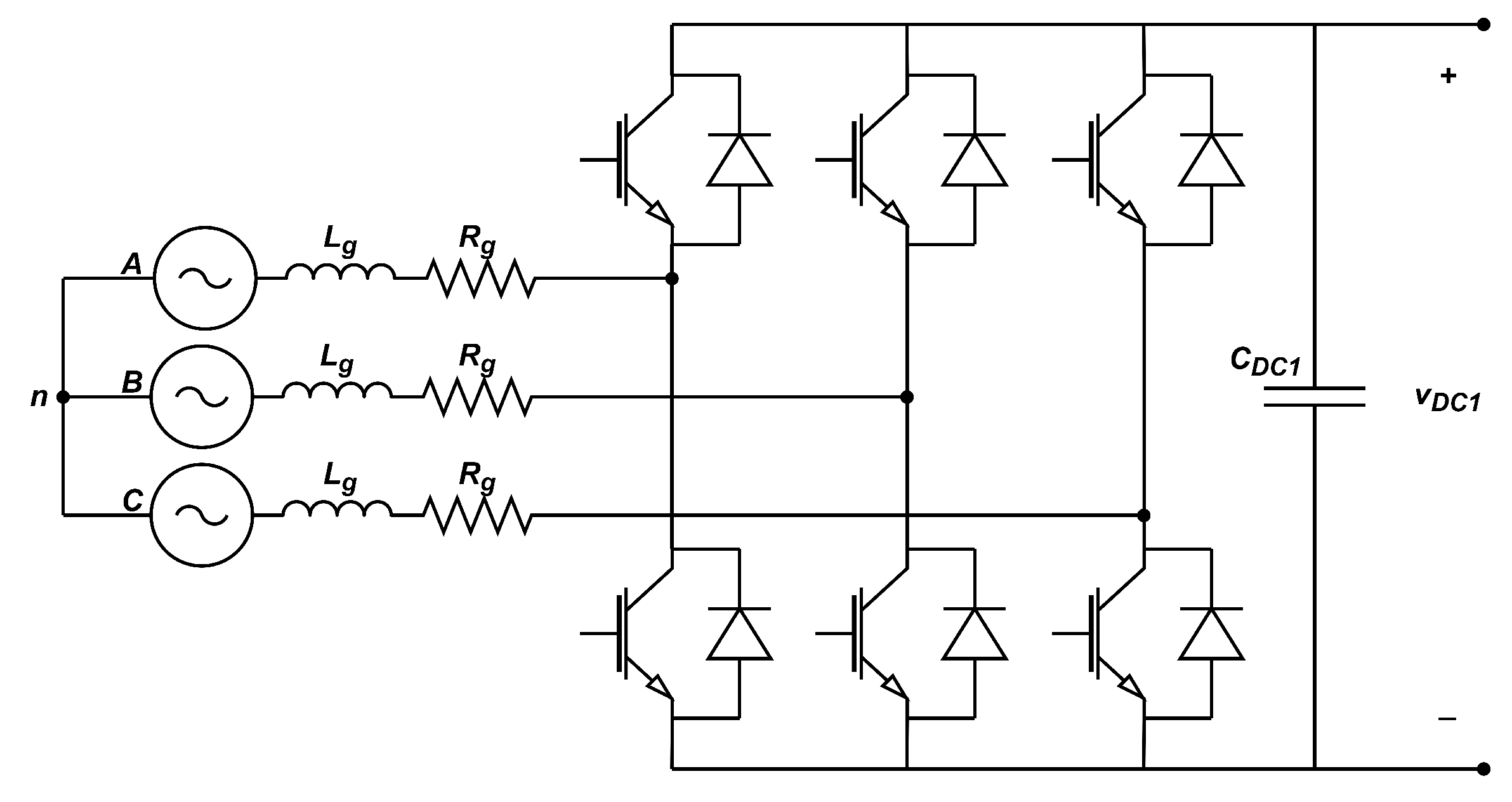
TM. The control design of the grid-connected AC-DC converter has been carried out in accordance with [29] and the input DC voltage v D C 1 
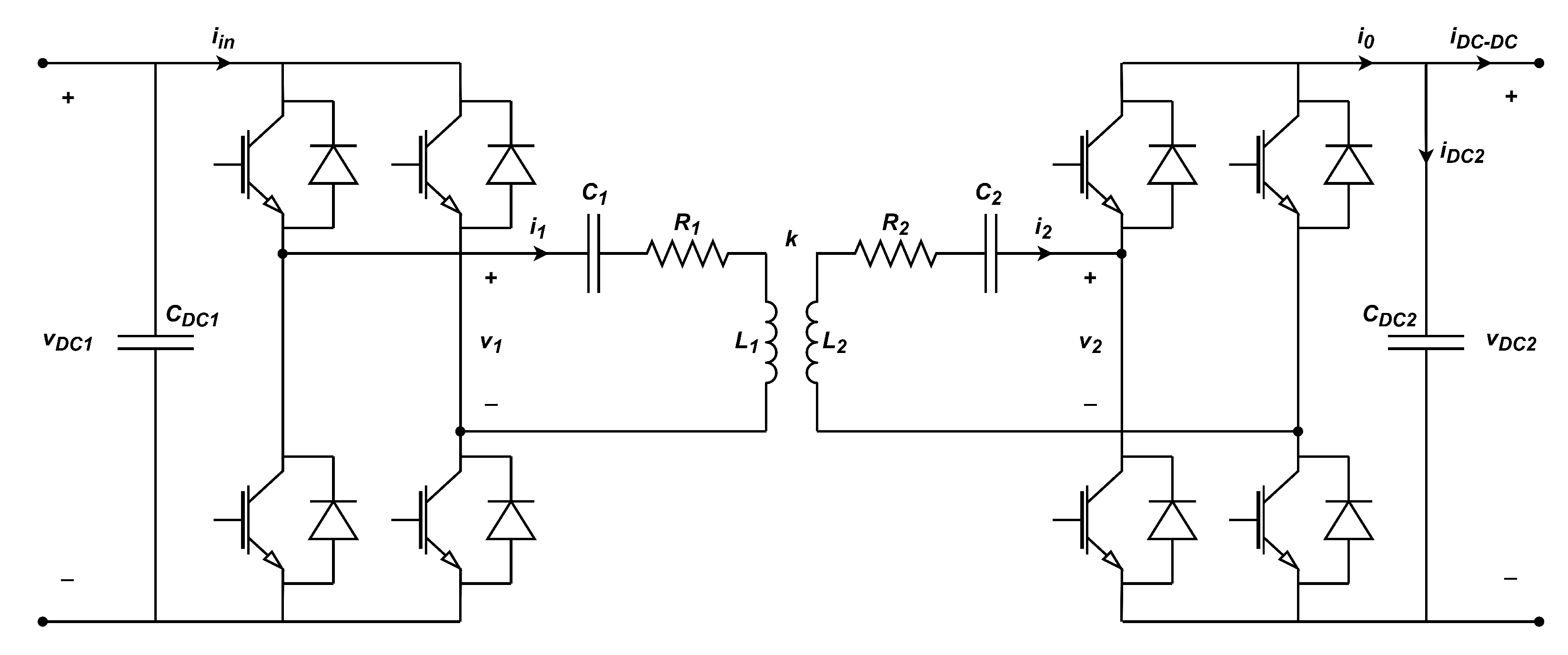
of the H-bridge converter associated with the primary side is set to 600 V. The switching frequency of the H-bridge converters associated with the IPT system is set to f r = 87.052 kHz, i.e., ω r = 174104 π rad/s: This value is in the range established by the SAE J2954 standard [
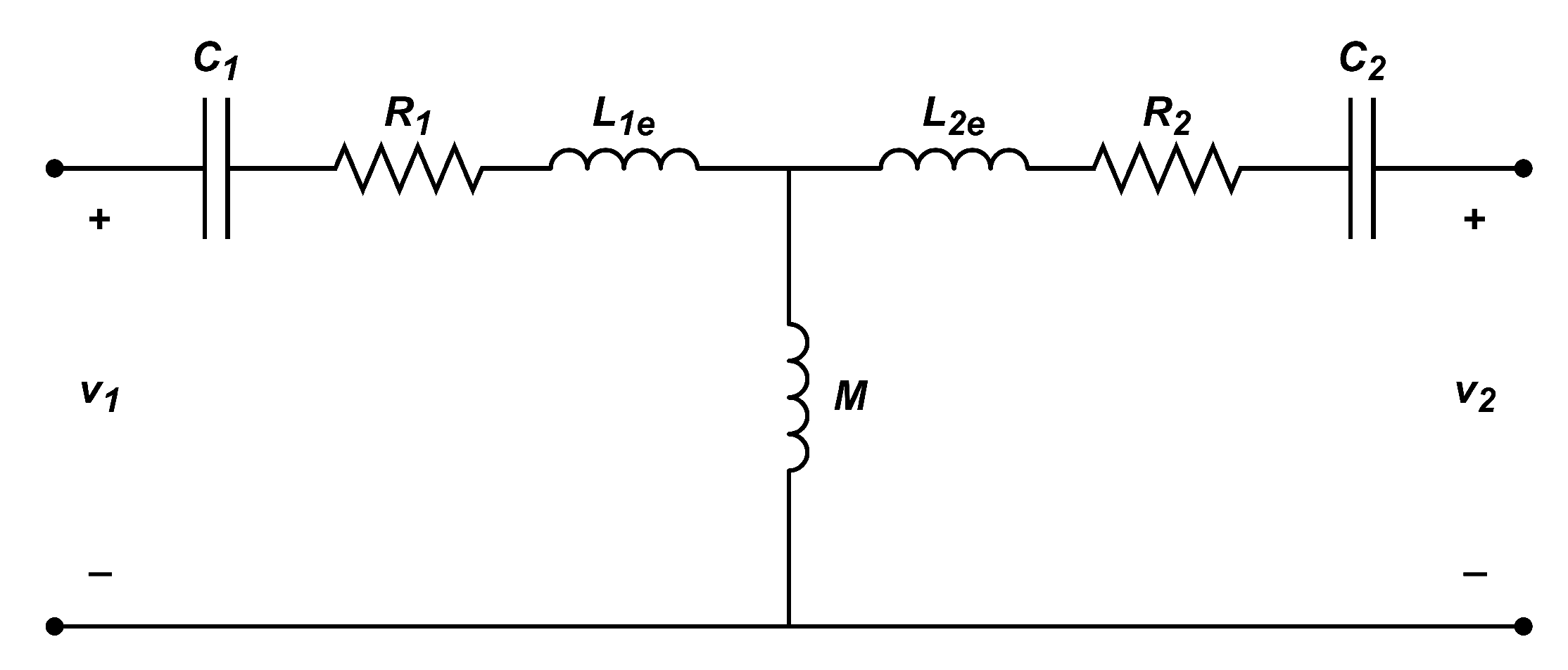
36]. The main parameters of the SS compensation system are summarized in Table 3. The switching frequency of the DC–DC step-down converter is chosen as 15 kHz, while the electromotive force and the internal series resistance of the battery are V b m = 200 V and R i = 0.2 Ω , respectively. The parameters of the control systems that regulate the DC voltage v D C 2 and the current of the battery i b are those obtained in the example explained in Section 4.3.
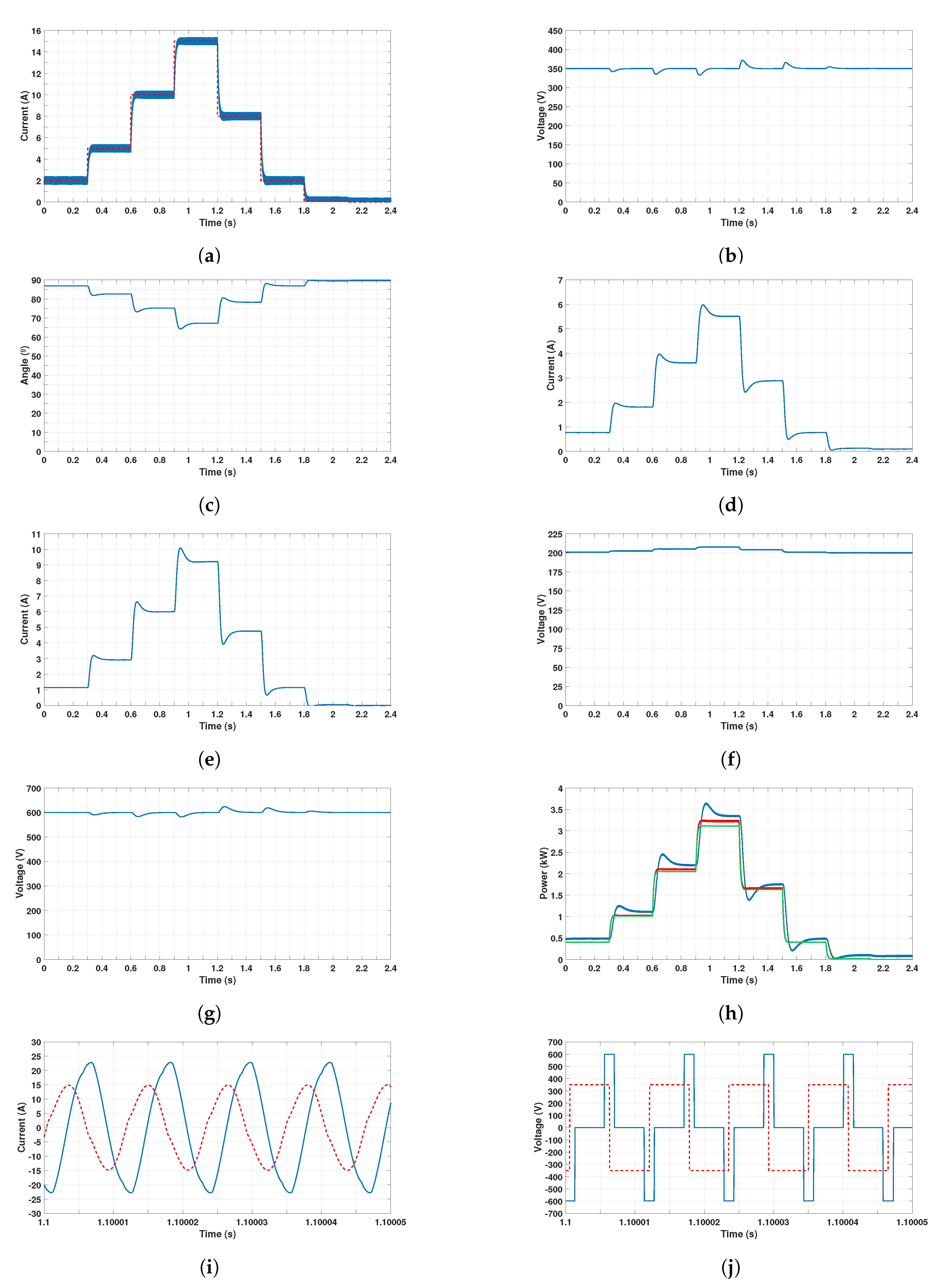
In order to test the performance of the designed control system, both the G2V mode and the V2G mode are simulated.

5.1. Simulation Results Obtained in the G2V Mode

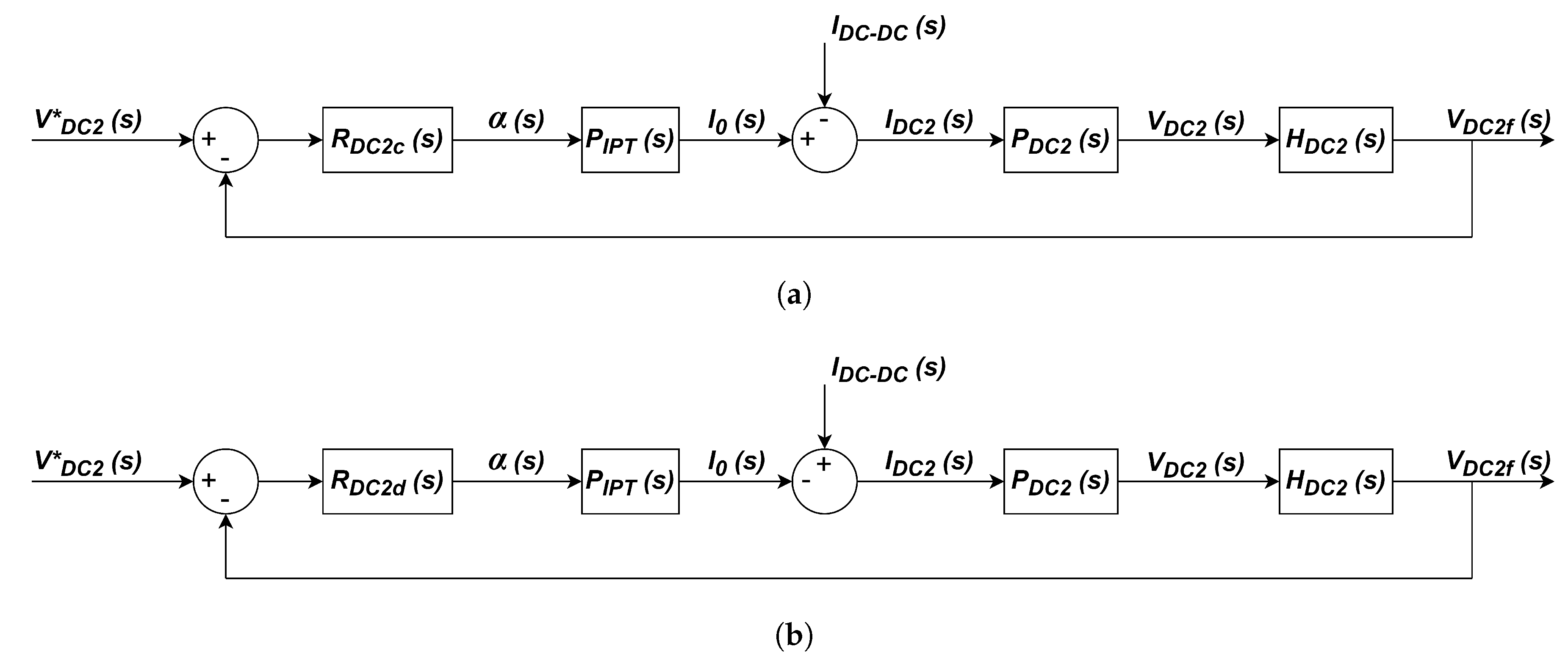
When the simulation test starts, both the control scheme of the DC voltage v D C 2 and the control system of the battery current i b are connected: The reference input for the voltage v D C 2 is set to 350 V, which is kept constant during the complete simulation time, and only the control scheme plotted in Figure 8a with the regulator R D C 2 c ( s ) is working. The value of the reference input for the battery current is changed as shown in Table 4. The total simulation time is 2.4 s.
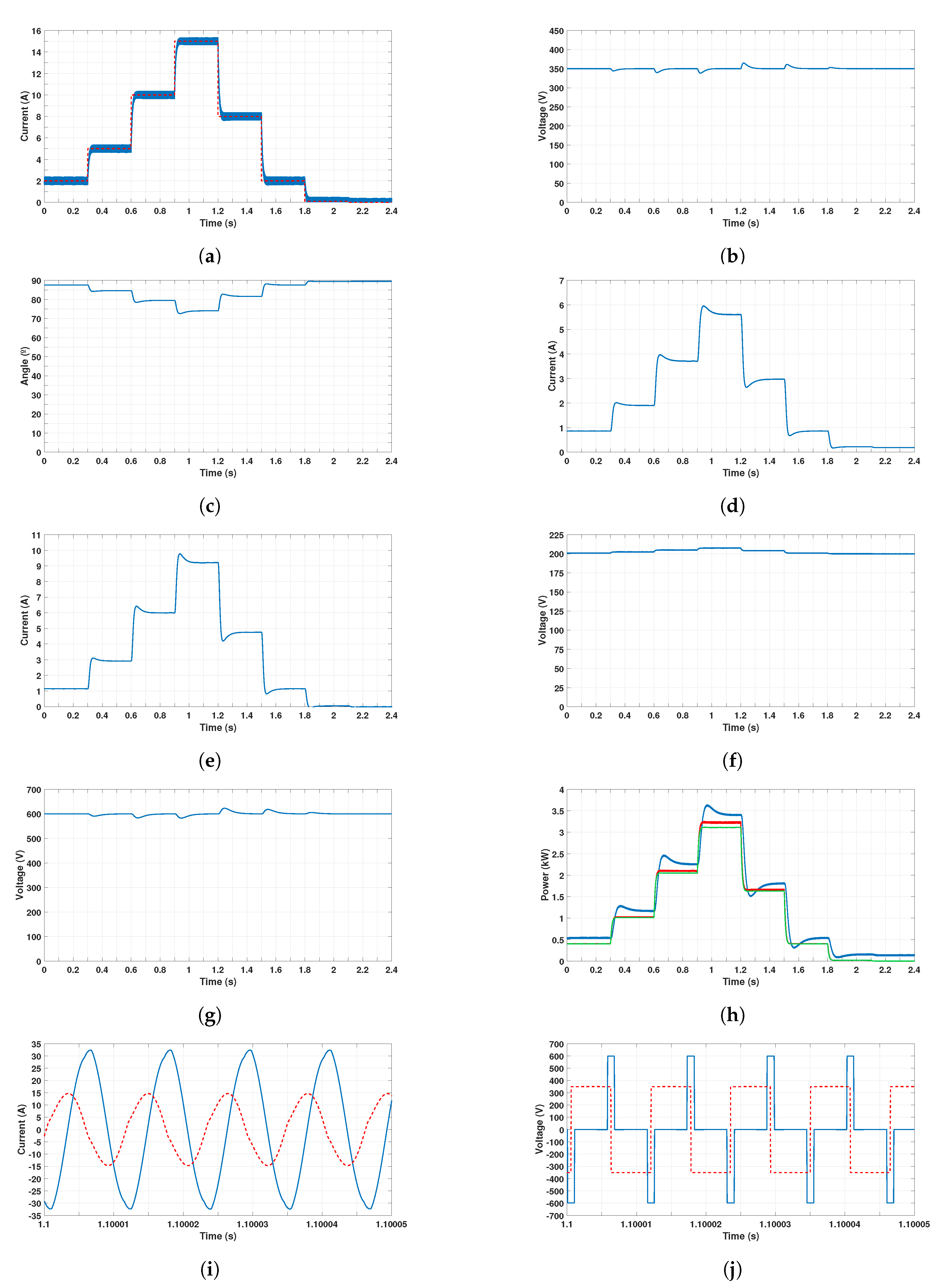
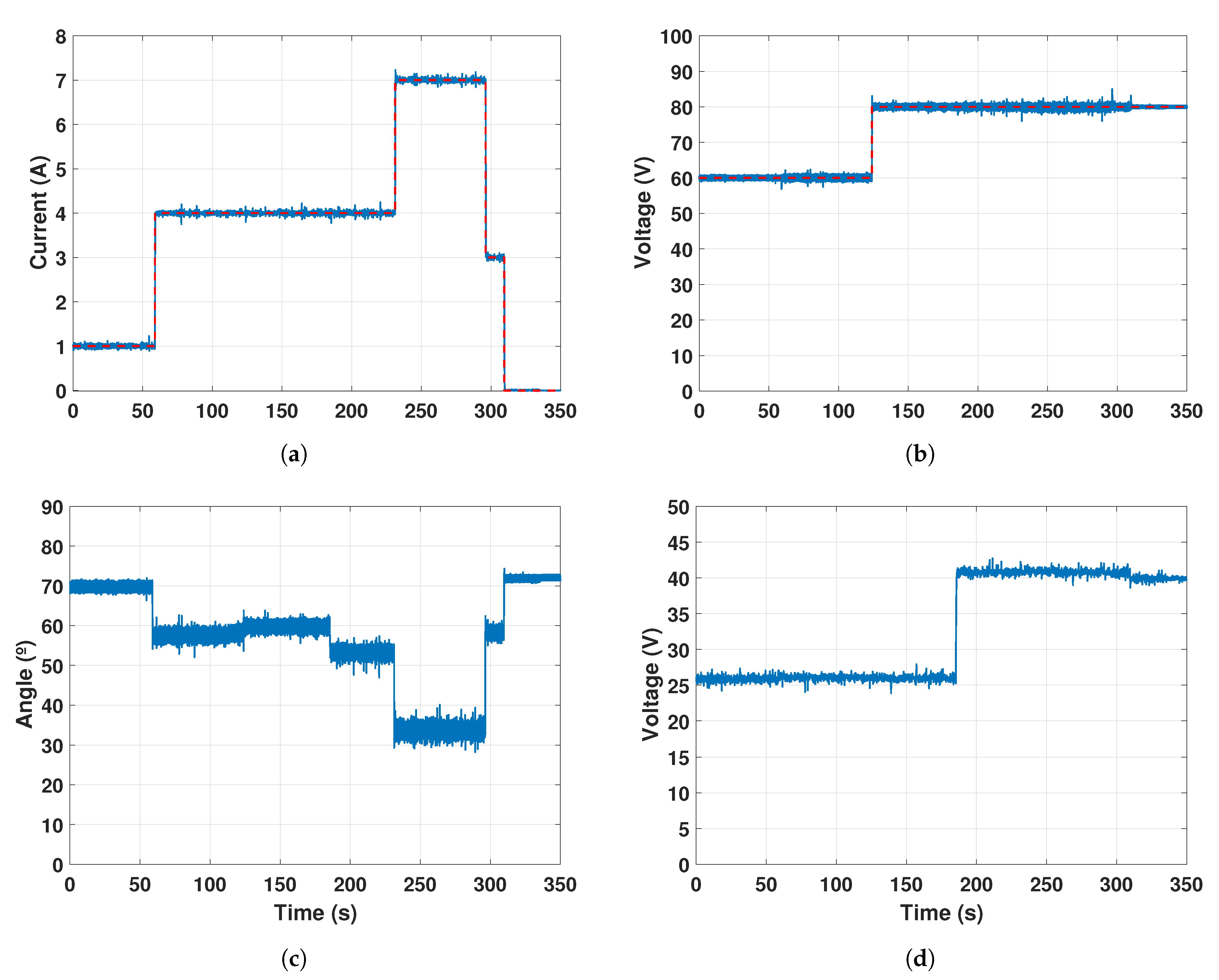
The obtained results are plotted in Figure 12. Figure 12a plots the time response of the current i b together with its reference: The steady state is reached within a maximum of 28 ms, without overshoot, and the tracking error is zero. For time instants, t = 1.8 s and t = 2.1 s the reference values are set to 0.1 A and 0 A, respectively. This scenario of small charging currents is normally present when the battery is charged at constant voltage. Once again, the control system maintains the battery current at the reference value in steady state.
The evolution of the voltage v D C 2 is shown in Figure 12b. Although the assumption that the various control systems are considered decoupled was made for the purpose of control design, they are slightly coupled, and changes in the battery current modify; therefore, the voltage v D C 2 and vice versa. This coupling effect is quantified by measuring the overshoot and the undershoot of the time response. The results show that the deviations of the voltage with regard to the reference value of 350 V are effectively corrected. As the control system of the voltage v D C 2 is nonlinear, different values for the overshoot and the 2%-settling time are obtained depending on the value of the battery current, yielding a maximum overshoot equal to 6.23 % , a minimum undershoot equal to 4.93 % , while the maximum 2%-settling time is 65.9 ms. This information is summarized in Table 5, showing that all the features of the voltage v D C 2 meet the design specifications. Furthermore, the tracking error in steady state is zero owing to the integral action for all the time intervals. The regulation of the voltage v D C 2 is achieved owing to the control of the phase-shift angle α in the output voltage of the H-bridge converter associated with the primary side, as shown in Figure 12c.
The input current through the H-bridge converter on the primary side i i n is plotted in Figure 12d, while the output current of the H-bridge converter on the secondary side i 0 is shown in Figure 12e: Both currents experience changes in accordance with the variations of the battery current i b . Moreover, Figure 12f shows the time response of the battery voltage v b , which is not constant owing to the voltage changes produced in the internal resistance R i .
Although the control of the voltage v D C 1 is not one of the goals of this paper, the time response of this voltage is shown in Figure 12g: The control system is able to maintain the DC voltage at 600 V with zero-tracking error regardless of the variations in the battery current. In accordance with Table 5, the maximum overshoot is 3.98 % , the minimum undershoot is 2.98 % , while the maximum 2%-settling time is 96 ms.
Figure 12h shows the evolution with time of the grid power P g , the input power of the DC–DC converter P d c and the battery power P b , which are used to compute the efficiency of the IPT system. In accordance with the SAE-J2954 standard [36], the efficiency is calculated from the grid connection to the input terminals of the vehicle energy storage system, i.e, the input of the DC–DC converter, which means that η s t = P d c / P g , while the efficiency of the complete IPT system should include the power dissipated in the DC–DC converter, yielding η g l o b a l = P b / P g . Table 6 shows the efficiencies η s t and η g l o b a l for each time interval of the simulation: the maximum efficiency value η s t is 96.55% and is achieved for i b = 15 A, while the efficiency is reduced drastically for i b = 0.1 A, i.e., a small value of the charging current. Although the efficiency is obtained in a simulation environment, the maximum achieved value is in accordance with those of some commercial contactless chargers featuring a similar rated power, which exhibit an efficiency in the interval of 89 % η s t 95.8 % , as explained in [7].
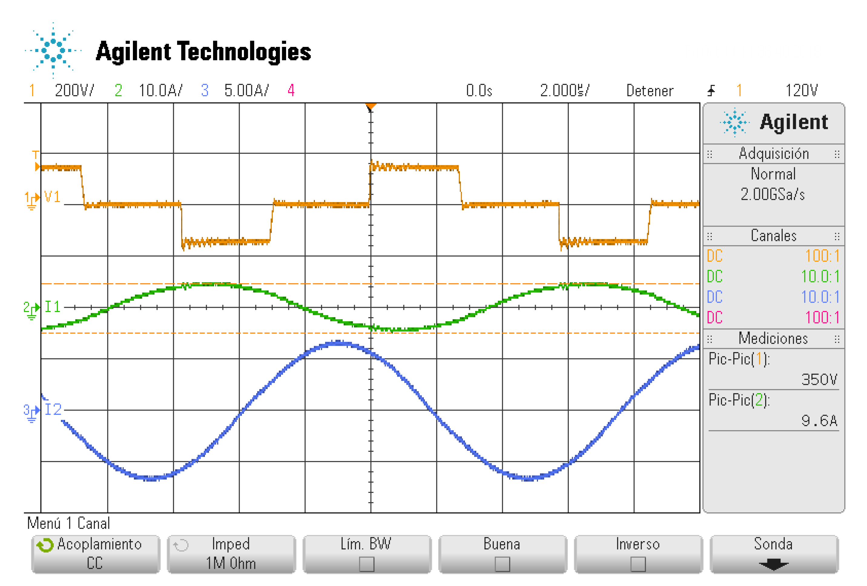
Figure 12i,j show the currents and the voltages, respectively, in steady state at the input and at the output of the compensated magnetic coupler. As the operating frequency of the IPT system is f r = 87.052 kHz, the time response is very fast compared with the total time simulation and only a time interval of 50 μ s is shown. The currents plotted in Figure 12i show that the current through the primary side i 1 contains some harmonic components, while the current through the secondary side i 2 is almost sinusoidal owing the filtering capability of the mutual inductance M. Furthermore, the phase-shift angle α of the input voltage on the primary side v 1 , i.e., the output voltage of the H-bridge converter on the primary side, can be observed in Figure 12j. The amplitude of v 1 
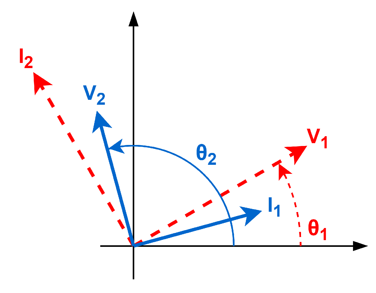
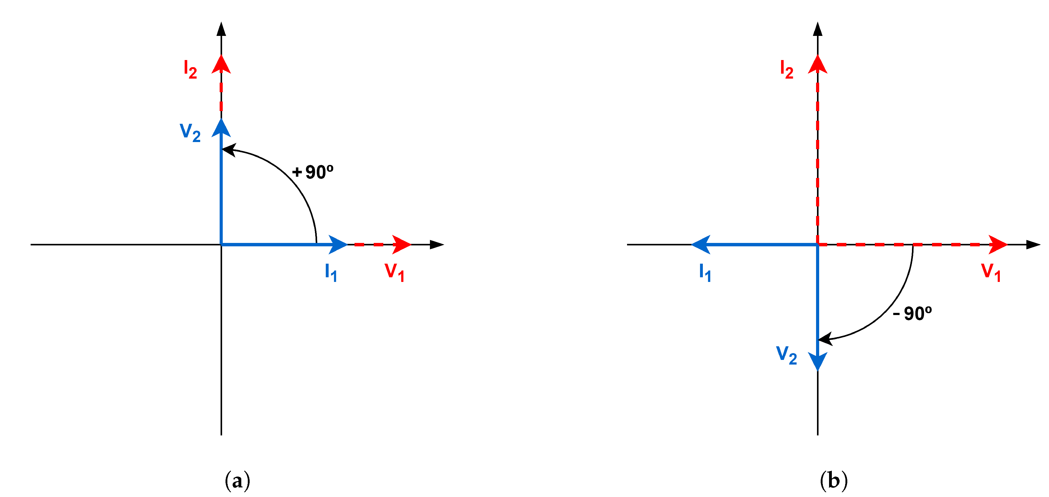
is 600 V, whereas the output voltage on the secondary side v 2 is a square waveform with amplitude 350 V, and is characterized by a phase lead of 90° with regard to v 1 , which implies that the system operates in the G2V mode, as explained in Section 3. Moreover, the currents and the voltages on both the primary side and the secondary side are in phase.

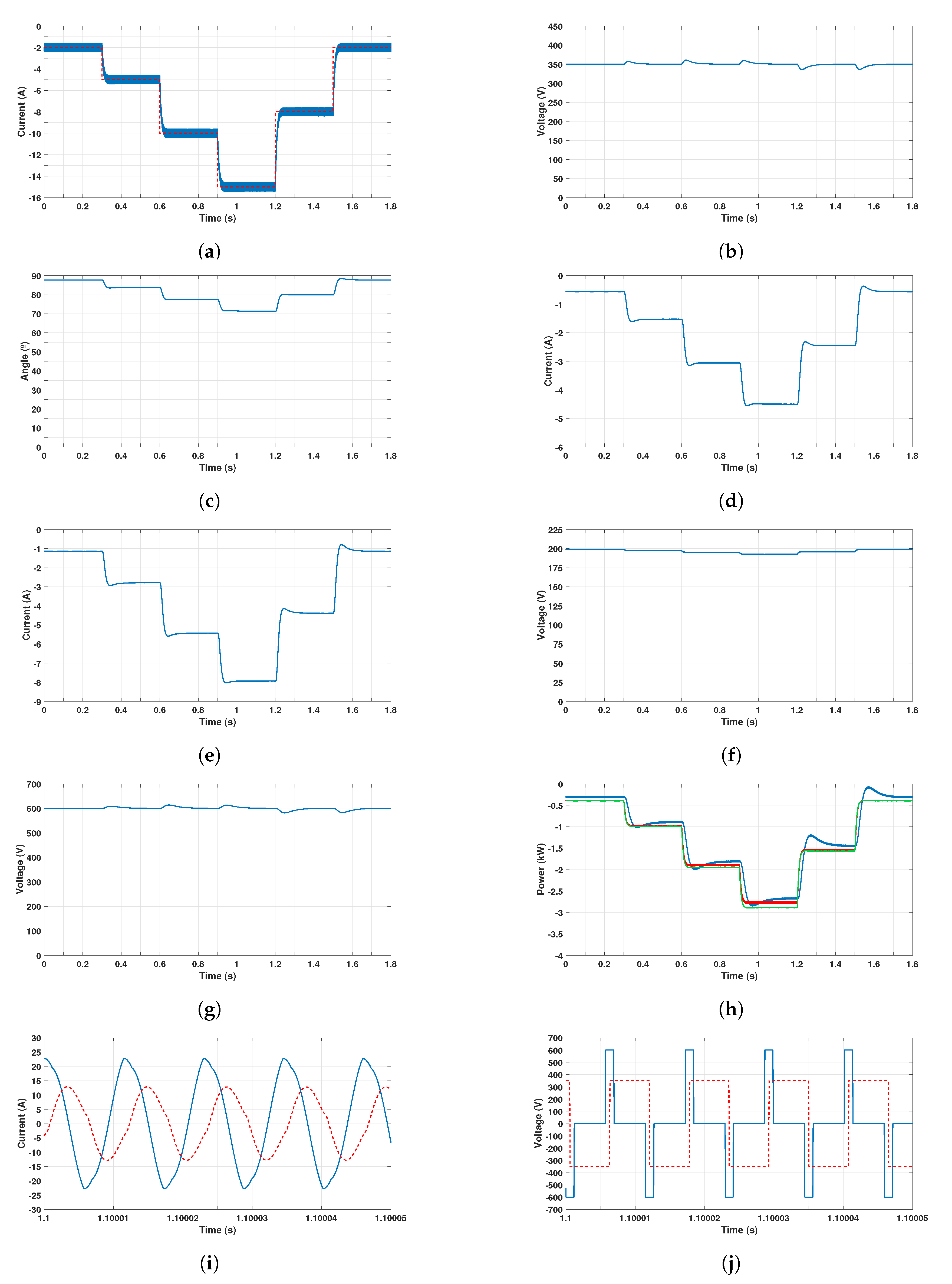
5.2. Simulation Results Obtained in the V2G Mode

In this case, the control scheme of the DC voltage v D C 2 plotted in Figure 8b, with the regulator R D C 2 d ( s ) , is connected. The reference input for the voltage v D C 2 is again set to 350 V and maintained constant. The control system of the current of the battery is also connected, but, in this case, the reference value is changed according to Table 7. The total time of the simulation is 1.8 s.
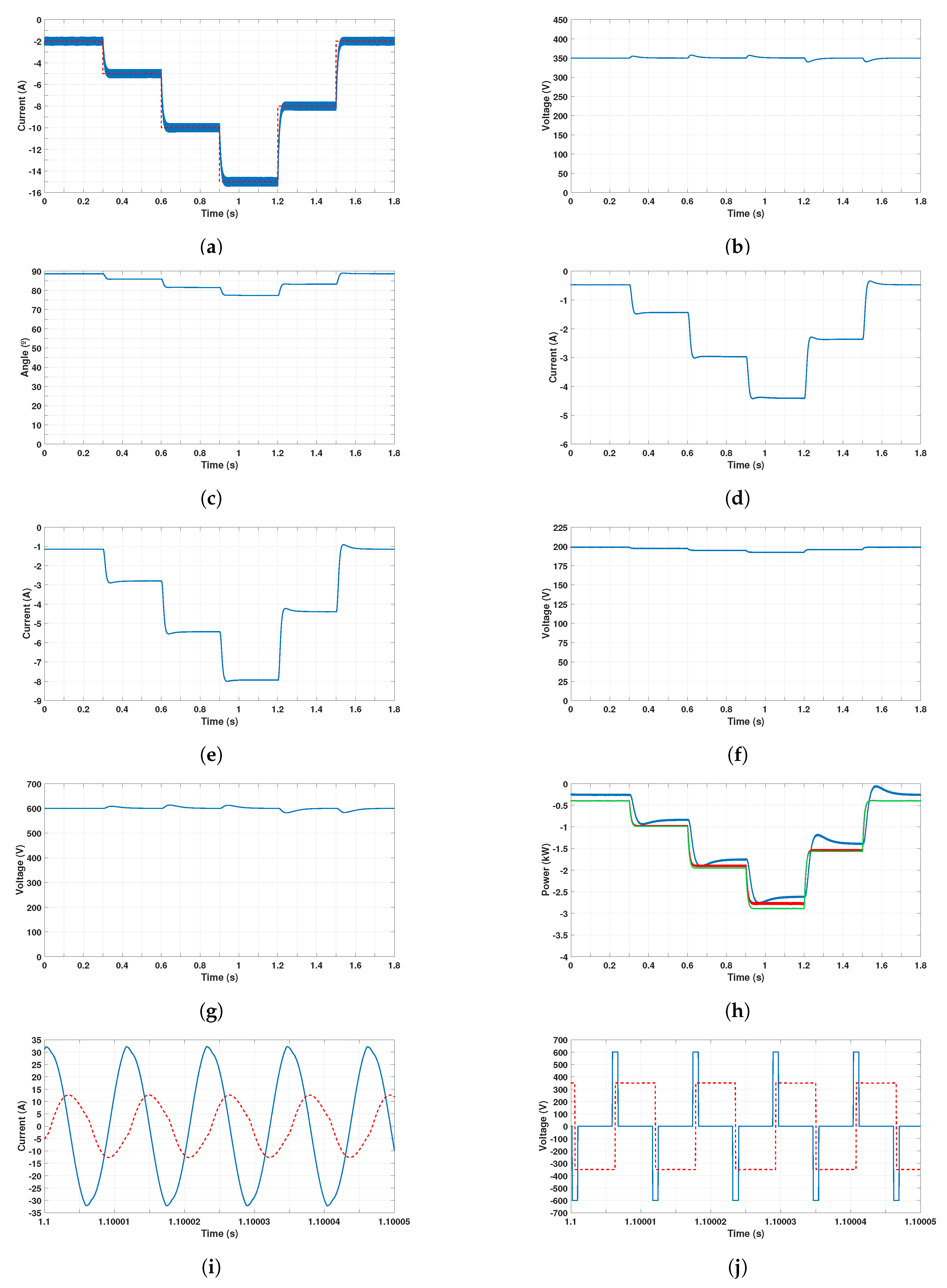
Figure 13 plots the results obtained in the V2G mode, while Table 8 contains the main parameters of the time responses of the variables i b , v D C 2 , and v D C 1 . The time response of the battery current i b is plotted in Figure 13a, in which the error in steady state is zero and the maximum 2%-settling time is 26.7 ms. Moreover, the time response does not exhibit overshoot.
Figure 13b shows the DC voltage v D C 2 of the secondary circuit: the maximum overshoot caused by changes in the battery current is 3.04%, while the minimum undershoot is −4.14%, and the maximum 2%-settling time is 57.7 ms. These figures provide evidence that the coupling between both control systems is within the range of the design requirements. Figure 13c plots the phase-shift angle α of the output voltage on the primary-side H-bridge converter. The angle α is varied by the controller R D C 2 d ( s ) to maintain the voltage v D C 2 around 350 V regardless of the variations caused by the changes in the battery current i b .
Figure 13d,e plot the time responses of the input current through the H-bridge converter on the primary side i i n and the output current of the H-bridge converter on the secondary side i 0 , respectively. As in the case of the G2V mode, the currents change their values in accordance with the changes in the battery current. Nonetheless, unlike the G2V mode, both currents are now negative as in the V2G mode the energy is extracted from the battery and injected into the grid. With regard to the evolution of the battery voltage v b , its time response is shown in Figure 13f: In this case, the voltage v b is lower below 200 V as the drop voltage in the internal resistance R i is negative owing to the negative sign of the battery current.
Figure 13g shows the time response of the DC voltage of the primary circuit v D C 1 . Once again, the voltage remains around 600 V despite the overshoots and undershoots caused by the changes in the current i b : The maximum overshoot is 2.26%, the minimum undershoot is −3.08% and the maximum 2%-settling time is 83.6 ms (see Table 8 for more details).
Figure 13h shows the grid power, the power at the input of the DC–DC converter and the power of the battery. As the power flow is now opposite to that of the G2V mode, i.e., from the battery to the grid, the efficiencies should be redefined in order to avoid values greater than 100%. For that reason, η s t = P g / P d c and η g l o b a l = P g / P b in the V2G mode. Table 9 summarizes the values of the efficiencies for the different time intervals: the maximum value for the efficiency η s t is 96.4%, which is achieved when the current of the battery is −15 A.
Finally, Figure 13i,j plot the currents and the voltages, respectively, in steady state at the input and at the output of the compensated magnetic coupler. Like in the G2V mode, only a time interval of 50 μ s is considered. Both currents contain harmonic components, although they can be considered relatively sinusoidal. Figure 13j shows that the output voltage of the H-bridge converter on the secondary side, v 2 , is generated with a phase lag of 90° with regard to the voltage v 1 in order to allow the system to be operated in the V2G mode (see Section 3 for more details). Furthermore, in the V2G case, one can observe that the currents and the voltages on both the primary side and the secondary side have opposite phases, as shown in Figure 7b.

5.3. Performance with Variations in the Coupling Factor

The design of the proposed control system requires a constant value for the coupling factor k, and the previous simulation results have been carried out assuming that the value of k used for the control design is equal to the actual value of the IPT system. Considering, however, that k is expected to fluctuate around an optimal value every time the EV batteries are charged (owing to misalignment issues); this requirement may seem difficult to achieve in a real-life wireless charging scenario. Fortunately, it is feasible to get around this limitation and still assume a constant k value in practice, recalling that previous works have recently demonstrated IPT systems especially designed to optimize the alignment of the coil coupling, either by using auxiliary sensing coils to detect the position of the EV [37] or by designing low-frequency ferrite rod antennas integrated into the primary and the secondary device [38]. Nevertheless, the performance of the control system should be investigated when the coupling factor undergoes deviations from its rated valued. In accordance with [39], where the influence of the misalignment on the coupling factor is analyzed, the previous simulation cases are repeated considering a decrease in the actual value of k of a 30% with regard to the rated value k n , i.e., k = 0.7 k n , while maintaining the same control parameters.
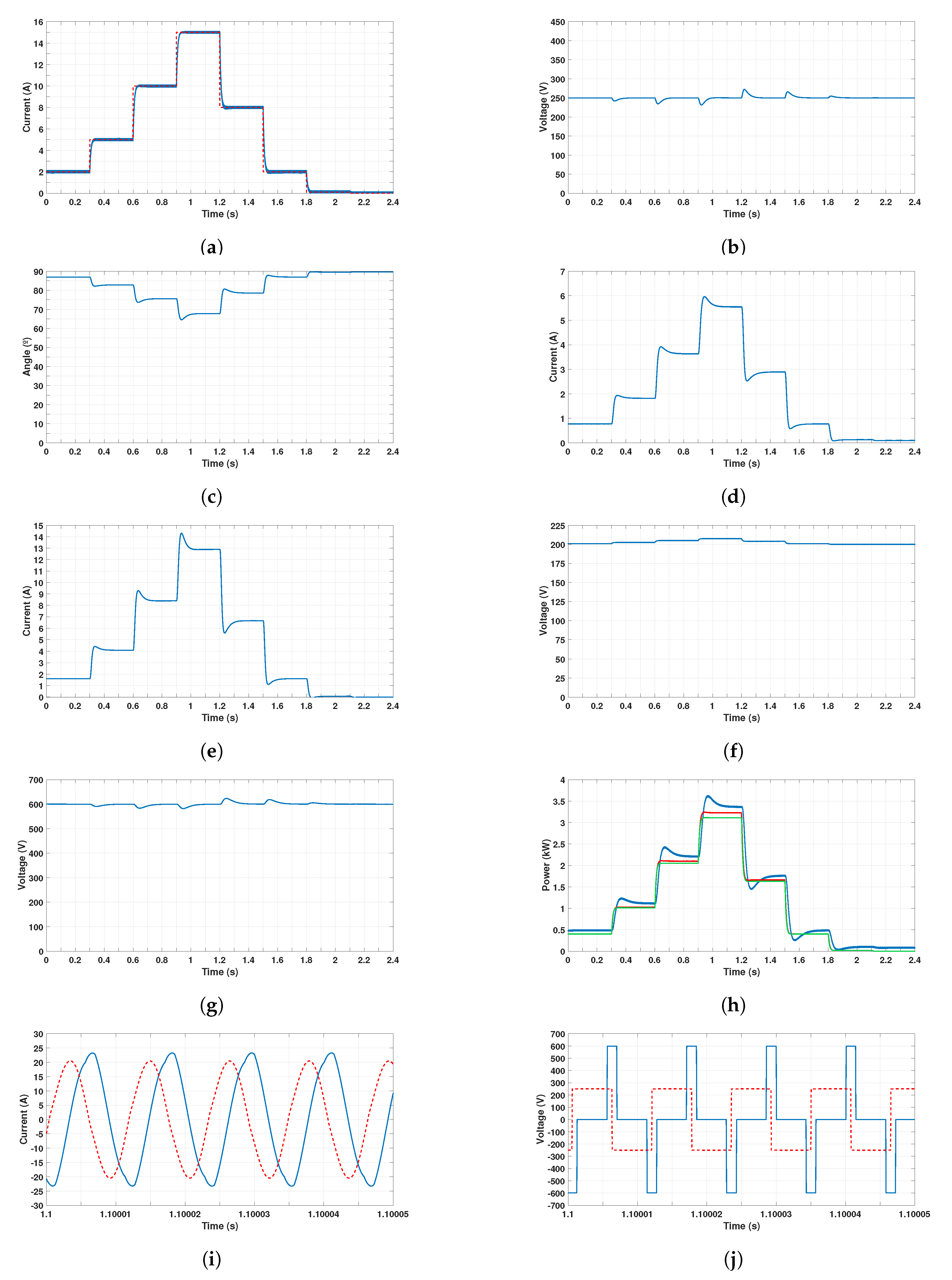
Figure 14 plots the results obtained working in the G2V mode with the same current profile and conditions as those specified in Section 5.1. The results reveal that the control performs effectively even for low values of the current i b , and the overall system is still stable even in the case of deviations from the rated k value as large as −30%. Nevertheless, a thorough analysis shows that the time response of the battery current i b (see Figure 14a) is slower than that plotted in Figure 12a, particularly for low values of i b where the settling time is 32.6 ms for i b = 2 A and 81.2 ms for i b = 0.1 A. The main features of the time responses of i b , v D C 2 and v D C 1 are summarized in Table 10. With regard to the time responses of v D C 2 and v D C 1 , after a comparison of the information contained in Table 5 and Table 10; the results obtained are very similar to those obtained using the rated valued of k, showing that the coupling between both control systems is similar, despite the decrease in k.
Efficiencies decrease, however, when k = 0.7 k n , yielding an increase in the power absorbed from the grid in order to maintain the power injected into the battery, as shown in Figure 14h. Table 11 contains the efficiency values and shows a maximum value for η s t equal to 94.9%, i.e., a reduction of 1.6% with regard to the case of k n .
Besides a lower efficiency, Figure 14i reveals the main drawback of working with a lower coupling factor than that used in the control design in SS-compensated IPT systems [13]: the current through the primary side of the magnetic coupler i 1 increases from a peak value of 22.5 A (see Figure 12i) to a peak value equal to 33.1 A. This increase reduces the efficiency and may even damage the power electronic converters if the current exceeds their rated values.
In order to avoid this drawback when k is lower than k n while operating safely the SS-compensated IPT systems, the voltage v D C 2 can be reduced, which implies a reduction in the current i 1 without the need of recalculating the control parameters. A new case study is carried out with the same conditions as the case study plotted in Figure 14, except for the reference v D C 2 * being reduced from 350 V to 250 V.
The results obtained are plotted in Figure 15 and the main features of the variables i b , v D C 2 and v D C 1 are also summarized in Table 10. The control system performs again effectively with k = 0.7 k n and v D C 2 = 250 V, although the time response of i b is slower than that obtained for the case study with rated coupling factor, with a 2%-settling time of 38.3 ms in the worst case. The time response of the voltage v D C 2 yields a maximum overshoot of 8.96%, a minimum undershoot of −7.41%, and a maximum 2%-settling time of 71.2 ms. These features are worse than those obtained with k n , yielding a higher coupling between both control systems. Nevertheless, the maximum overshoot is still within the range of the design specification, showing that the design of the control system is robust. The time response of the voltage v D C 1 exhibits similar features to those obtained with k n .
Efficiencies improve their values with regard to the case of k = 0.7 k n and v D C 2 = 350 V, as shown in Table 11, and they are very similar to those obtained with k n (see Table 6). Furthermore, the peak value of current i 1 has been decreased, as shown in Figure 15i, allowing, thus, a safe operation of the IPT system.
The case study of the V2G mode detailed in Section 5.2 is also tested when k = 0.7 k n . The results obtained are plotted in Figure 16. The global system is also stable in the V2G mode, and the control performs very effectively and yields a good regulation of the current i b (see Figure 16a) and the voltages v D C 2 and v D C 1 , as shown in Figure 16b,g, respectively.
The main drawback is, once again, the increase in the primary side current of the compensated magnetic coupler i 1 , owing to the SS compensation employed in the IPT system. In order to avoid this disadvantage, the voltage v D C 2 is reduced, yielding, therefore, a decrease in the current i 1 , like in the case of the G2V mode.
Table 12 shows the main parameters of the time responses of the variables i b , v D C 2 and v D C 1 . The 2%-settling time of the current i b is slower than that obtained for the rated value of the coupling factor k n , with a maximum value of 32.5 ms. Nevertheless, variables v D C 2 and v D C 1 exhibit similar properties to those obtained with k n , which implies that a decrease in k does not have a significant influence on the coupling of the voltages v D C 2 and v D C 1 caused by the changes in the battery current. Furthermore, efficiencies are summarized in Table 13, which shows lower values compared to those achieved when k = k n : The efficiency η s t is reduced up to 2% from its maximum value.

6. Experimental Results

The proposed control schemes for the current i b and the voltage v D C 2 have been tested with a preliminary laboratory prototype that currently allows the unidirectional battery charging process to be fully tested. The scheme of the prototype is shown in Figure 17: At the current stage of development, the prototype is not fed from the grid yet, and so the DC voltage v D C 1 is supplied by three series-connected XP Power DNR480PS48-I power sources with an overall voltage of 144 V. The bidirectional H-bridge converter was constructed from two single-leg converters with Silicon Carbide (Sic) MOSFETs (Ref. KIT8020CRD8FF1217P-1) manufactured by CREE and characterized by a peak reverse voltage of 1200 V and an average forward current of 10 A. The inductive coupling has been built in accordance with the SAE-J2954 standard and its parameters were already summarized in Table 3. At this early stage of the development, a bridge rectifier is used in the secondary circuit instead a bidirectional H-bridge converter. The bridge rectifier was built by connecting two semiconductor modules (ref. STTH6006TV), and each module includes two ultrafast diodes characterized by a peak reverse voltage of 600 V and an average forward current of 30 A. The capacitor C D C 2 has a capacitance of 1360 μ F and its maximum voltage is rated at 800 V. The DC–DC converter is implemented by using one leg of the modular three-phase inverter SKS 22FB6U+E1CIF+B6CI 13 V12, supplied by SEMIKRON, and is connected to the BE10 battery emulator manufactured by Cinergia by means of an inductive filter L b R b whose values were already defined in Table 1. The measurement of the battery current i b is provided by the Hall-effect sensor LA55P (manufactured by LEM), while the measurement of the voltage v D C 2 is provided by the Hall-effect sensor LV-25P (LEM). The controllers were implemented on the dSPACE MicroLabBox real-time platform using a sampling frequency of 15 kHz. The switching frequency of the H-bridge converter was set to f s w 1 = 87.05 kHz, which is in the range established by the SAE-J2954 standard, whereas the switching frequency of the DC–DC converter is f s w 2 = 15 kHz.
An experiment was carried out to confirm the performance of the controllers for the current i b and the voltage v D C 2 when the IPT system operates in the G2V mode. When the experiment begins, the reference of the current i b is set to 1 A, the reference of the voltage v D C 2 is set to 60 V, and the voltage of the battery emulator V b m is set to 25 V. The profile of the current reference is modified along the time, with an initial step from 1 A to 4 A, a second step from 4 A to 7 A, a third step from 7 A to 3 A, and a final step in which the reference is decreased from 3 A to 0 A. The reference v D C 2 * is changed from 60 V to 80 V when the current reference is i b * = 4 A. The change occurs at a time instant between 100 s and 150 s. Furthermore, the voltage of the battery emulator V b m is changed from 25 V to 40 V at a time instant between 150 s and 200 s. The total time of the experiment is 350 s.
Figure 18 shows the results obtained for this experiment. The control system is able to track the reference of the current without overshoot, even when the current of the battery is zero and when the voltage of the battery is increased, as shown in Figure 18a. Figure 18b shows the profile of the voltage v D C 2 : The regulator R D C 2 c modifies the phase-shift angle of the output voltage of the H-bridge converter in order to make the voltage v D C 2 tracks its reference. The evolution of the phase-shift angle is plotted in Figure 18c, while the voltage of the battery emulator is plotted in Figure 18d, which shows the variations of v b in accordance with the variations of the current i b . The results also show that the overall control scheme is able to operate the IPT system under low values of the battery current, which is often the case when the battery is charged at constant voltage.
Finally, Figure 19 plots the currents through the compensated magnetic coupler i 1 and i 2 . These waveforms are almost sinusoidal. Figure 19 also shows the output voltage of the H-bridge converter, in which the phase-shift angle can be observed.

7. Conclusions

In this paper, the design of the control system of a bidirectional IPT system for EVs connected to the electrical grid has been presented. The complete control system is split into various subsystems, namely, the control scheme of the DC voltage of the primary circuit and the reactive power exchanged with the grid; the control subsystem of the DC voltage of the secondary circuit and the control scheme of the current through the EV battery. Furthermore, the selection of the G2V and V2G modes is carried out by introducing a phase-shift of ± 90 ° in the secondary voltage of the IPT system with regard to the primary voltage. Although the IPT system employs an SS compensation topology, the use of the well-known root–locus technique applied to the control design methodology allows for extending the design of the control system when other compensation topologies are used. The control design procedure has been thoroughly explained in order to provide a method that can be easily applied by designers in IPT based applications. Simulation results are obtained by using PSCADTM/EMTDCTM operating in both the G2V and V2G modes. The results show that both the overshoot and undershoot caused by the coupling between the different control systems are always within the range of the design specifications, which implies that the designed control is effective. One of the advantages of the proposed control scheme is its robustness against a mismatch between the coupling factor k used in the model and the actual one. Furthermore, under an increase in the current through the primary side of the magnetic coupler i 1 , the control scheme can guarantee the safe operation of the SS-compensated IPT system by reducing the DC voltage on the secondary side, yielding, therefore, a decrease in the current i 1 . Consequently, the basic SS compensation topology used in this work is an appropriate choice for the design of IPT chargers, as its performance and robustness are similar to those of more complex compensation topologies, provided the charging operation is supervised by a reliable control system as the one demonstrated in this work. The simulation and experimental results show a satisfactory performance of the control system with zero-tracking error in steady state and a fast transient response when the IPT system operates in both modes.

8. Future Work

Although the performance of the control system has been fully tested through simulation results, some of the proposed features have not been experimentally validated owing to the early stage of the laboratory prototype, such as the operation in the V2G mode. Once the prototype is completely built, experimental results of the overall performance of the control system working in the V2G mode will be obtained.

Author Contributions

Conceptualization, E.J.M.-M. and P.R.-S.; methodology, E.J.M.-M. and P.R.-S.; software, E.J.M.-M. and F.J.L.-A.; validation, E.J.M.-M. and F.J.L.-A.; formal analysis, E.J.M.-M. and A.P.T.; investigation, E.J.M.-M.; resources, P.R.-S. and J.V.; data curation, E.J.M.-M. and F.J.L.-A.; writing—original draft preparation, E.J.M.-M. and P.R.-S.; writing—review and editing, J.V., A.P.T., and F.J.L.-A.; visualization, E.J.M.-M.; supervision, P.R.-S. and J.V.; project administration, P.R.-S.; funding acquisition, P.R.-S. All authors have read and agreed to the published version of the manuscript.

Funding

This research received no external funding.

Conflicts of Interest

The authors declare no conflict of interest. The funders had no role in the design of the study; in the collection, analyses, or interpretation of data; in the writing of the manuscript, or in the decision to publish the results.

Abbreviations

The following abbreviations are used in this manuscript:
EVElectric Vehicle
G2VGrid-to-Vehicle
V2GVehicle-to-Grid
WPTWireless Power Transfer
IPTInductive Power Transfer
CPTCapacitive Power Transfer
VSIVoltage-Source Inverter
CCMContinuos Conduction Mode
PIProportional-Integral

References

  1. Neukom, R.; Steiger, N.; Gómez-Navarro, J.; Wang, J.; Werner, J. No evidence for globally coherent warm and cold periods over the preindustrial Common Era. Nature 2019, 571, 550–554. [Google Scholar] [CrossRef]
  2. Neukom, R.; Barboza, L.; Erb, M.; Shi, F.; Emile-Geay, J.; Evans, M.; Franke, J.; Kaufman, D.; Lücke, L.; Rehfeld, K.; et al. Consistent multidecadal variability in global temperature reconstructions and simulations over the Common Era. Nat. Geosci. 2019, 12, 643–649. [Google Scholar] [PubMed]
  3. Blunden, J.; Arndt, D.S. State of the Climate in 2018. Bull. Am. Meteorol. Soc. 2019, 100, Si-S306. [Google Scholar] [CrossRef] [Green Version]
  4. Lindsey, R. Climate Change: Atmospheric Carbon Dioxide; National Oceanographic and Atmospheric Administration: Washington, DC, USA, 2020. [Google Scholar]
  5. Agency, E.E. Annual European Union Approximated Greenhouse Gas Inventory for the Year 2018; Publications Office of the European Union: Luxembourg, 2019. [Google Scholar]
  6. Jadhav, A. Wireless Electric Vehicle Charging Market by Power Source, Charging Method, Installation, Distribution Channel and Vehicle Type—Global Opportunity Analysis and Industry Forecast, 2020–2030. Allied Mark. Res. (Allied Anal. LLP) 2020. [Google Scholar]
  7. Bosshard, R.; Kolar, J.W. Inductive power transfer for electric vehicle charging: Technical challenges and trade-offs. IEEE Power Electron. Mag. 2016, 3, 22–30. [Google Scholar] [CrossRef]
  8. Li, S.; Li, W.; Deng, J.; Nguyen, T.D.; Mi, C.C. A Double-Sided LCC Compensation Network and Its Tuning Method for Wireless Power Transfer. IEEE Trans. Veh. Technol. 2015, 64, 2261–2273. [Google Scholar] [CrossRef]
  9. Madawala, U.K.; Thrimawithana, D.J. Current sourced bi-directional inductive power transfer system. IET Power Electron. 2011, 4, 471–480. [Google Scholar] [CrossRef]
  10. Liu, F.; Yang, Y.; Jiang, D.; Ruan, X.; Chen, X. Modeling and Optimization of Magnetically Coupled Resonant Wireless Power Transfer System With Varying Spatial Scales. IEEE Trans. Power Electron. 2017, 32, 3240–3250. [Google Scholar] [CrossRef]
  11. Patil, D.; McDonough, M.K.; Miller, J.M.; Fahimi, B.; Balsara, P.T. Wireless Power Transfer for Vehicular Applications: Overview and Challenges. IEEE Trans. Transp. Electrif. 2018, 4, 3–37. [Google Scholar] [CrossRef]
  12. Lu, F.; Zhang, H.; Mi, C. A Review on the Recent Development of Capacitive Wireless Power Transfer Technology. Energies 2017, 10, 1752. [Google Scholar] [CrossRef] [Green Version]
  13. Del Toro García, X.; Vázquez, J.; Roncero-Sánchez, P. Design, implementation issues and performance of an inductive power transfer system for electric vehicle chargers with series–series compensation. IET Power Electron. 2015, 8, 1920–1930. [Google Scholar] [CrossRef]
  14. Wang, C.S.; Stielau, O.H.; Covic, G.A. Design considerations for a contactless electric vehicle battery charger. IEEE Trans. Ind. Electron. 2005, 52, 1308–1314. [Google Scholar] [CrossRef]
  15. Vázquez, J.; Roncero-Sánchez, P.; Torres, A.P. Coupling factor of a weak inductive coupling in a 2-kW power transfer system with a 125-mm air gap for electric vehicle chargers. In Proceedings of the 2017 IEEE 26th International Symposium on Industrial Electronics (ISIE), Scotland, UK, 19–21 June 2017; pp. 670–675. [Google Scholar]
  16. Buja, G.; Bertoluzzo, M.; Mude, K.N. Design and Experimentation of WPT Charger for Electric City Car. IEEE Trans. Ind. Electron. 2015, 62, 7436–7447. [Google Scholar] [CrossRef]
  17. Yao, Y.; Liu, X.; Wang, Y.; Xu, D. LC/CL compensation topology and efficiency-based optimisation method for wireless power transfer. IET Power Electron. 2018, 11, 1029–1037. [Google Scholar] [CrossRef]
  18. Liu, C.; Ge, S.; Guo, Y.; Li, H.; Cai, G. Double-LCL resonant compensation network for electric vehicles wireless power transfer: Experimental study and analysis. IET Power Electron. 2016, 9, 2262–2270. [Google Scholar] [CrossRef]
  19. Madawala, U.K.; Thrimawithana, D.J. A Bidirectional Inductive Power Interface for Electric Vehicles in V2G Systems. IEEE Trans. Ind. Electron. 2011, 58, 4789–4796. [Google Scholar] [CrossRef]
  20. Varikkottil, S.; Febin Daya, J.L. High-gain LCL architecture based IPT system for wireless charging of EV. IET Power Electron. 2019, 12, 195–203. [Google Scholar] [CrossRef]
  21. Samanta, S.; Rathore, A.K.; Thrimawithana, D.J. Bidirectional Current-Fed Half-Bridge (C) (LC)–(LC) Configuration for Inductive Wireless Power Transfer System. IEEE Trans. Ind. Appl. 2017, 53, 4053–4062. [Google Scholar] [CrossRef]
  22. Yan, Z.; Zhang, Y.; Song, B.; Zhang, K.; Kan, T.; Mi, C. An LCC-P Compensated Wireless Power Transfer System with a Constant Current Output and Reduced Receiver Size. Energies 2019, 12, 172. [Google Scholar] [CrossRef] [Green Version]
  23. Kim, M.; Joo, D.; Lee, B.K. Design and Control of Inductive Power Transfer System for Electric Vehicles Considering Wide Variation of Output Voltage and Coupling Coefficient. IEEE Trans. Power Electron. 2019, 34, 1197–1208. [Google Scholar] [CrossRef]
  24. Neath, M.J.; Swain, A.K.; Madawala, U.K.; Thrimawithana, D.J.; Vilathgamuwa, D.M. Controller Synthesis of a Bidirectional Inductive Power Interface for electric vehicles. In Proceedings of the 2012 IEEE Third International Conference on Sustainable Energy Technologies (ICSET), Kathmandu, Nepal, 24–27 September 2012; pp. 60–65. [Google Scholar]
  25. Hou, J.; Chen, Q.; Wong, S.; Tse, C.K.; Ruan, X. Analysis and Control of Series/Series-Parallel Compensated Resonant Converter for Contactless Power Transfer. IEEE J. Emerg. Sel. Top. Power Electron. 2015, 3, 124–136. [Google Scholar]
  26. Qu, X.; Han, H.; Wong, S.; Tse, C.K.; Chen, W. Hybrid IPT Topologies With Constant Current or Constant Voltage Output for Battery Charging Applications. IEEE Trans. Power Electron. 2015, 30, 6329–6337. [Google Scholar] [CrossRef]
  27. Mohamed, A.A.S.; Marim, A.A.; Mohammed, O.A. Magnetic Design Considerations of Bidirectional Inductive Wireless Power Transfer System for EV Applications. IEEE Trans. Magn. 2017, 53, 1–5. [Google Scholar] [CrossRef]
  28. Li, Z.; Zhu, C.; Jiang, J.; Song, K.; Wei, G. A 3-kW Wireless Power Transfer System for Sightseeing Car Supercapacitor Charge. IEEE Trans. Power Electron. 2017, 32, 3301–3316. [Google Scholar] [CrossRef]
  29. Roncero-Sánchez, P.; Torres, A.P.; Vázquez, J. Control scheme of a concentration photovoltaic plant with a hybrid energy storage system connected to the grid. Energies 2018, 11, 301. [Google Scholar] [CrossRef] [Green Version]
  30. Vázquez, J.; Roncero-Sánchez, P.; Torres, A.P. Simulation model of a 2-kW IPT charger with phase-shift control: Validation through the tuning of the coupling factor. Electronics 2018, 7, 255. [Google Scholar] [CrossRef] [Green Version]
  31. Mohan, N.; Undeland, T.M.; Robbins, W.P. Power Electronics: Converters, Applications and Design, 3rd ed.; Wiley-IEEE Press: Hoboken, NJ, USA, 2002. [Google Scholar]
  32. De La Cruz, C.; Lema, M.B.; Del Toro García, X.; Roncero-Sánchez, P. Energy Storage Integration with Renewable Energies: The Case of Concentration Photovoltaic Systems; Handbook of Environmental Chemistry; Springer: Berlin/Heidelberg, Germany, 2016; Volume 34, pp. 73–94. [Google Scholar]
  33. Nise, N.S. Control Systems Engineering; Wiley: New York, NY, USA, 2011. [Google Scholar]
  34. Smith, C.A.; Corripio, A. Principles and Practice of Automatic Process Control, 3rd ed.; Wiley: West Sussex, UK, 2005. [Google Scholar]
  35. Hart, D.W. Power Electronics, international ed.; McGraw-Hill: New York, NY, USA, 2011. [Google Scholar]
  36. Standard, S. Wireless Power Transfer for Light-Duty Plug-in/Electric Vehicles and Alignment Methodology; SAE J2954 TIR; SAE: Warrendale, PA, USA, 2019. [Google Scholar]
  37. Babu, A.; George, B. Sensor System to Aid the Vehicle Alignment for Inductive EV Chargers. IEEE Trans. Ind. Electron. 2019, 66, 7338–7346. [Google Scholar] [CrossRef]
  38. Seong, J.Y.; Lee, S.S. Optimization of the Alignment Method for an Electric Vehicle Magnetic Field Wireless Power Transfer System Using a Low-Frequency Ferrite Rod Antenna. Energies 2019, 12, 4689. [Google Scholar] [CrossRef] [Green Version]
  39. López-Alcolea, F.J.; Vazquez del Real, J.; Roncero-Sánchez, P.; Parreño Torres, A. Modeling of a Magnetic Coupler Based on Single- and Double-Layered Rectangular Planar Coils with In-Plane Misalignment for Wireless Power Transfer. IEEE Trans. Power Electron. 2020, 35, 5102–5121. [Google Scholar] [CrossRef]
Figure 1. General scheme of the proposed IPT bidirectional system connected to the grid.
Electronics 09 01724 g001
Figure 2. Scheme of the AC–DC converter connected to the grid.
Electronics 09 01724 g002
Figure 3. Compensated magnetic coupler and its associated bidirectional H-bridge converters.
Electronics 09 01724 g003
Figure 4. T-model employed for the magnetic coupler.
Electronics 09 01724 g004
Figure 5. Bidirectional step-down DC–DC converter connected to the battery of the EV.
Electronics 09 01724 g005
Figure 6. Phasor diagram of variables V ¯ 1 , V ¯ 2 , I ¯ 1 and I ¯ 2 .
Electronics 09 01724 g006
Figure 7. Phasor diagrams for both operation modes. (a) phasor diagram for the G2V mode; (b) phasor diagram for the V2G mode.
Electronics 09 01724 g007
Figure 8. Block diagrams of the control subsystem for regulating the DC voltage V D C 2 ( s ) . (a) control system for the G2V operation mode; (b) control system for the V2G operation mode.
Electronics 09 01724 g008
Figure 9. Closed-loop scheme for the control of the current of the EV battery I b ( s ) .
Electronics 09 01724 g009
Figure 10. (a) locations of the closed-loop poles for the control subsystem of the voltage v D C 2 ; (b) time responses of the voltage v D C 2 for a unit step in the reference v D C 2 * ; (c) time responses of the voltage v D C 2 for a unit step in the disturbance i D C D C .
Electronics 09 01724 g010
Figure 11. (a) location of the poles of the closed-loop system for the control of the battery current i b ; (b) time response of the battery current i b without considering the filter H b ( s ) (blue) and including the filter (red).
Electronics 09 01724 g011
Figure 12. Results obtained for the G2V mode. Time responses of: (a) the battery current i b (blue) and the reference i b * (red); (b) the DC voltage v D C 2 ; (c) the phase-shift angle α ; (d) the current i i n ; (e) the current i 0 ; (f) the voltage of the battery v b ; (g) the DC voltage v D C 1 ; (h) the grid power P g (blue), the power at the input of the DC–DC converter P d c (red) and the battery power P b (green); (i) currents of the compensated magnetic coupler i 1 (blue), and i 2 (red); (j) voltages across the compensated magnetic coupler v 1 (blue), and v 2 (red).
Electronics 09 01724 g012
Figure 13. Results obtained for the V2G mode. Time responses of (a) the battery current i b (blue) and the reference i b * (red); (b) the DC voltage v D C 2 ; (c) the phase-shift angle α ; (d) the current i i n ; (e) the current i 0 ; (f) the voltage of the battery v b ; (g) the DC voltage v D C 1 ; (h) the grid power P g (blue), the power at the input of the DC–DC converter P d c (red) and the battery power P b (green); (i) currents of the compensated magnetic coupler i 1 (blue), and i 2 (red); (j) voltages across the compensated magnetic coupler v 1 (blue), and v 2 (red).
Electronics 09 01724 g013
Figure 14. Results obtained for the G2V mode when k = 0.7 k n and v D C 2 * = 350 V. Time responses of: (a) the battery current i b (blue) and the reference i b * (red); (b) the DC voltage v D C 2 ; (c) the phase-shift angle α ; (d) the current i i n ; (e) the current i 0 ; (f) the voltage of the battery v b ; (g) the DC voltage v D C 1 ; (h) the grid power P g (blue), the power at the input of the DC–DC converter P d c (red) and the battery power P b (green); (i) currents of the compensated magnetic coupler i 1 (blue), and i 2 (red); (j) voltages across the compensated magnetic coupler v 1 (blue), and v 2 (red).
Electronics 09 01724 g014
Figure 15. Results obtained for the G2V mode when k = 0.7 k n and v D C 2 * = 250 V. Time responses of: (a) the battery current i b (blue) and the reference i b * (red); (b) the DC voltage v D C 2 ; (c) the phase-shift angle α ; (d) the current i i n ; (e) the current i 0 ; (f) the voltage of the battery v b ; (g) the DC voltage v D C 1 ; (h) the grid power P g (blue), the power at the input of the DC–DC converter P d c (red) and the battery power P b (green); (i) currents of the compensated magnetic coupler i 1 (blue), and i 2 (red); (j) voltages across the compensated magnetic coupler v 1 (blue), and v 2 (red).
Electronics 09 01724 g015
Figure 16. Results obtained for the V2G mode when k = 0.7 k n . Time responses of: (a) the battery current i b (blue) and the reference i b * (red); (b) the DC voltage v D C 2 ; (c) the phase-shift angle α ; (d) the current i i n ; (e) the current i 0 ; (f) the voltage of the battery v b ; (g) the DC voltage v D C 1 ; (h) the grid power P g (blue), the power at the input of the DC–DC converter P d c (red) and the battery power P b (green); (i) currents of the compensated magnetic coupler i 1 (blue), and i 2 (red); (j) voltages across the compensated magnetic coupler v 1 (blue), and v 2 (red).
Electronics 09 01724 g016
Figure 17. Scheme of the laboratory prototype.
Electronics 09 01724 g017
Figure 18. Experimental results. Time responses of: (a) the battery current i b (blue) and the reference i b * (red); (b) the voltage v D C 2 (blue) and the reference v D C 2 * (red); (c) the regulation of the phase-shift angle α carried out by the regulator R D C 2 c ( s ) ; (d) the voltage of the battery v b .
Electronics 09 01724 g018
Figure 19. Currents through the compensated magnetic coupler: primary side current i 1 (green), secondary side current i 2 (blue). Output voltage of the H-bridge converter (orange).
Electronics 09 01724 g019
Table 1. Parameters employed to obtain the transfer functions P I P T ( s ) , P D C 2 ( s ) and P b ( s ) .
ParameterValue
α 0 (°)60
V D C 1 (V)600
ω r (rad/s)174104 π
M ( μ H)36.35
t I P T (ms)4.6
τ (ms)0.92
C D C 2 ( μ F)1360
L b (mH)7
R b ( Ω )0.5
Table 2. Pole values of the closed-loop system for the control of the voltage v D C 2 .
PolesLocation (Rad/s)
p 1 −34.7
p 2 −185.17
p 3 −203.17
p 4 −1163.92
Table 3. Parameters of the SS compensation system.
ParameterValue
Compensation capacitor C 1 (nF)22.6
Self-inductance L 1 ( μ H)144.5
Stray resistance R 1 (m Ω )183
Compensation capacitor C 2 (nF)22.6
Self-inductance L 2 ( μ H)146.8
Stray resistance R 2 (m Ω )149
Coupling factor k0.2496
Table 4. Values of the current reference i b * throughout the time of the simulation. G2V mode.
Time Interval (s)Reference Value (A)
0.0 t < 0.3 2
0.3 t < 0.6 5
0.6 t < 0.9 10
0.9 t < 1.2 15
1.2 t < 1.5 8
1.5 t < 1.8 2
1.8 t < 2.1 0.1
2.1 t < 2.4 0
Table 5. Overshoot ( M p > 0 ) or undershoot ( m p < 0 ), and 2%-settling time ( t s ) in the G2V mode for i b , v D C 2 , and v D C 1 .
i b v DC 2 v DC 1
Time Interval (s) t s (ms) M p or m p (%) t s (ms) M p or m p (%) t s (ms)
0.3 t < 0.6 23.7−2.3236.2−1.580
0.6 t < 0.9 24.9−4.2957.2−2.7979.4
0.9 t < 1.2 22.3−4.9360.8−2.9883.9
1.2 t < 1.5 25.86.2365.93.9896.0
1.5 t < 1.8 26.74.5958.33.1684.8
1.8 t < 2.1 28.01.3600.960
2.1 t < 2.4 0.0700.060
Table 6. Efficiencies calculated in the G2V mode.
Time Interval (s) η st (%) η global (%)
0 t < 0.3 83.983.5
0.3 t < 0.6 92.591.4
0.6 t < 0.9 95.793.4
0.9 t < 1.2 96.593.2
1.2 t < 1.5 95.193.2
1.5 t < 1.8 83.683.2
1.8 t < 2.1 20.319.7
2.1 t < 2.4
Table 7. Values of the current reference i b * throughout the time of the simulation V2G mode.
Time Interval (s)Reference Value (A)
0.0 t < 0.3 −2
0.3 t < 0.6 −5
0.6 t < 0.9 −10
0.9 t < 1.2 −15
1.2 t < 1.5 −8
1.5 t < 1.8 −2
Table 8. Overshoot ( M p > 0 ) or undershoot ( m p < 0 ), and 2%-settling time ( t s ) in the V2G mode for i b , v D C 2 , and v D C 1 .
i b v DC 2 v DC 1
Time Interval (s) t s (ms) M p or m p (%) t s (ms) M p or m p (%) t s (ms)
0.3 t < 0.6 23.81.9701.430
0.6 t < 0.9 24.93.0445.42.2663.7
0.9 t < 1.2 21.22.8242.62.1258.1
1.2 t < 1.5 25.9−4.1457.7−3.0883.6
1.5 t < 1.8 26.7−3.9555.4−2.8779.9
Table 9. Efficiencies calculated in the V2G mode.
Time Interval (s) η st (%) η global (%)
0 t < 0.3 80.279.8
0.3 t < 0.6 91.690.4
0.6 t < 0.9 95.493.0
0.9 t < 1.2 96.492.6
1.2 t < 1.5 94.392.4
1.5 t < 1.8 79.979.4
Table 10. Overshoot ( M p > 0 (%)) or undershoot ( m p < 0 (%)), and 2%-settling time ( t s (ms)) in the G2V mode for i b , v D C 2 , and v D C 1 considering k = 0.7 k n .
v DC 2 * = 350 V v DC 2 * = 250 V
i b v D C 2 v D C 1 i b v D C 2 v D C 1
Time Interval (s) t s M p or m p t s M p or m p t s t s M p or m p t s M p or m p t s
0.3 t < 0.6 23.7−1.630−1.54023.7−3.2743.8−1.550
0.6 t < 0.9 24.9−2.9641.2−2.7175.024.7−6.2160.8−2.7675.8
0.9 t < 1.2 22.8−3.3145.4−2.7878.822.1−7.4161.6−2.9880.1
1.2 t < 1.5 26.84.2952.13.8493.526.88.9671.23.9293.9
1.5 t < 1.8 32.63.2342.93.0781.732.36.4465.13.0982.0
1.8 t < 2.1 81.20.9400.94038.31.8900.940
2.1 t < 2.4 0.0500.0500.1100.050
Table 11. Efficiencies calculated in the G2V mode when k = 0.7 k n .
Time Interval (s) v DC 2 * = 350 V v DC 2 * = 250 V
η st (%) η global (%) η st (%) η global (%)
0 t < 0.3 75.174.883.182.8
0.3 t < 0.6 88.187.092.191.0
0.6 t < 0.9 93.191.095.292.3
0.9 t < 1.2 94.991.695.992.5
1.2 t < 1.5 92.190.394.792.9
1.5 t < 1.8 75.475.083.583.1
1.8 t < 2.1 12.612.220.820.2
2.1 t < 2.4
Table 12. Overshoot ( M p > 0 ) or undershoot ( m p < 0 ), and 2%-settling time ( t s ) in the V2G mode for i b , v D C 2 , and v D C 1 considering k = 0.7 k n .
i b v DC 2 v DC 1
Time Interval (s) t s (ms) M p or m p (%) t s (ms) M p or m p (%) t s (ms)
0.3 t < 0.6 23.61.4101.400
0.6 t < 0.9 24.82.1927.22.2159.7
0.9 t < 1.2 21.22.0322.42.0853.0
1.2 t < 1.5 26.5−2.9540.7−3.0180.8
1.5 t < 1.8 32.5−2.8139.0−2.8076.8
Table 13. Efficiencies calculated in the V2G mode when k = 0.7 k n .
Time Interval (s) η st (%) η global (%)
0 t < 0.3 66.065.7
0.3 t < 0.6 86.185.0
0.6 t < 0.9 92.590.1
0.9 t < 1.2 94.490.7
1.2 t < 1.5 90.588.7
1.5 t < 1.8 65.465.1
Publisher’s Note: MDPI stays neutral with regard to jurisdictional claims in published maps and institutional affiliations.

