Effects of Extreme Thermal Shock on Microstructure and Mechanical Properties of Au-12Ge/Au/Ni/Cu Solder Joint


1
College of Materials Science and Technology, Nanjing University of Aeronautics and Astronautics, Nanjing 210016, China
2
State Key Laboratory of Advanced Brazing Filler Metals and Technology, Zhengzhou Research Institute of Mechanical Engineering, Zhengzhou 450001, China
3
Institute of Advanced Brazing Materials and Technology, China Innovation Academy of Intelligent Equipment Co., Ltd., Ningbo 315700, China
*
Author to whom correspondence should be addressed.
Metals 2020, 10(10), 1373; https://doi.org/10.3390/met10101373
Submission received: 27 September 2020
/
Revised: 12 October 2020
/
Accepted: 13 October 2020
/
Published: 15 October 2020
Abstract
:Extreme temperature change has generally been the great challenge to spacecraft electronic components, particularly in long, periodic, deep-space exploration missions. Hence, researchers have paid more attention to the reliability of component packaging materials. In this study, the microstructure evolution on the interface of Cu/Ni/Au/Au-12Ge/Au/Ni/Cu joints, as well as the effects of extreme thermal shock on mechanical properties and the fracture mode in the course of extreme thermal changes between −196 and 150 °C, have been investigated. Results revealed that the interface layers comprised of two thin layers of NiGe and Ni5Ge3 compounds after Au-12Ge solder alloy was soldered on the Au/Ni/Cu substrate. After extreme thermal shock tests, the microstructure morphology converted from scallop type to planar one due to the translation from NiGe to Ni5Ge3. Meanwhile, the thickness of interface layer hardly changed. The shear strength of the joints after 300 cycles of extreme thermal shock was 35.1 MPa, which decreased by 19.61%. The fracture location changed from the solder to solder/NiGe interface, and then to the interface of NiGe/Ni5Ge3 IMC layer. Moreover, the fracture type of the joints gradually transformed from ductile fracture mode to brittle mode during thermal shock test. Simultaneously, the formation and extension of defects, such as micro-voids and micro-cracks, were found during the process of thermal shock due to the different thermal expansion coefficient among the solder, interface layer and substrate.
1. Introduction
Restriction of Hazardous Substances (RoHS) and Waste Electrical and Electronic Equipment (WEEE) have restricted the use of conventional Sn-Pb solder due to the perniciousness of lead to the environment and the human body [1,2,3]. The research on lead-free solder has become an important issue [4,5]. Au-based solders are gradually regarded as an interesting candidate due to their excellent electrical and thermal conductivity and high fatigue resistance, thus being widely used in high-temperature packaging [6,7,8,9]. Among all Au-based solders, eutectic Au-12Ge (wt.%) alloy has become of interest for applications in highly loaded components and space technology devices due to its excellent comprehensive performances [10]. The Au-Ge binary system features eutectic temperature of 361 °C [11], which is suitable to high-reliability electronic assembly. Additionally, Au-12Ge alloy possesses many interesting properties such as excellent corrosion and oxidation resistance, thermal fatigue resistance, combined with high joint strength [12]. Therefore, Au-12Ge solder has been the critical packaging material for advanced microelectronic devices, especially the die attachment and micro-electro-mechanical systems (MEMS) devices package [13]. Furthermore, Au-12Ge alloy can meet the requirements of electrical conductivity and high reliability in high-power and high-integration applications, so it is especially suitable for connection of the silicon carbide power devices, microwave circuit and wafer bonding. High material costs are likely to limit the applicability of Au-12Ge solder in low-end electronic devices [14]. On the contrary, it is broadly applied in power chip modules of aerospace electronics.
Nowadays, deep space exploration has become a significant issue concerning society, economy, science and technology and other aspects of human development [15,16,17]. Compared with the conventional environment, spacecraft electronic components will experience significant temperature changes during service, such as, under the condition of Moon (−180 to 150 °C), Venus (−170 to 270 °C) and Giant Planets (−140 to 380 °C). These service conditions will severely damage the solder joint reliability and menace the safety of aerospace craft equipment. Previously, some researchers have investigated the influences of cryogenic temperatures and cryogenic temperatures thermal cycling on the mechanical properties, fracture behavior and microstructure evolution of the solder joint, which indicates that the overall performance of the devices will degrade to a certain extent [18,19]. Nonetheless, the failure mechanism and the relationship between the fracture and microstructure evolution under extreme environment is not yet precise. At the same time, the available information on mechanical properties, microstructure evolution at the interface and the reliability of Au-12Ge solder joints in the extreme environment remains insufficient [20]. Hence, it is essential to investigate the effect of extreme thermal shock on Au-12Ge solder joint, which might provide the theoretical reference for the application of Au-12Ge solder in space electronic devices.
In this study, Cu/Ni/Au/Au-12Ge/Au/Ni/Cu joints were prepared and underwent high- and low-temperature thermal shock to investigated the effect of temperature change on the microstructure evolution and mechanical property of joints. Thereinto, both the Au and Cu layer were the coatings on Cu substrates. Overall, the microstructure and shear strength of Au-12Ge solder joints subjected to extreme thermal shock were investigated, and the fracture morphologies of solder joints at different cycles of shock were analyzed in this study [21,22].
2. Materials and Methods
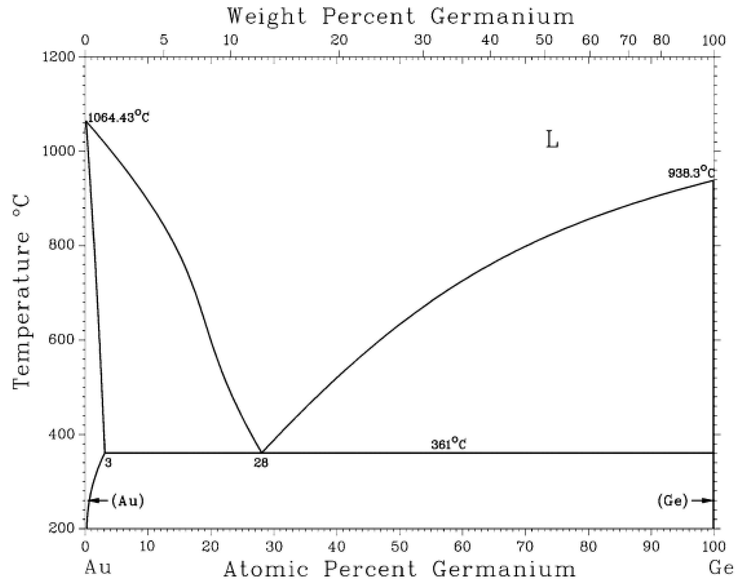
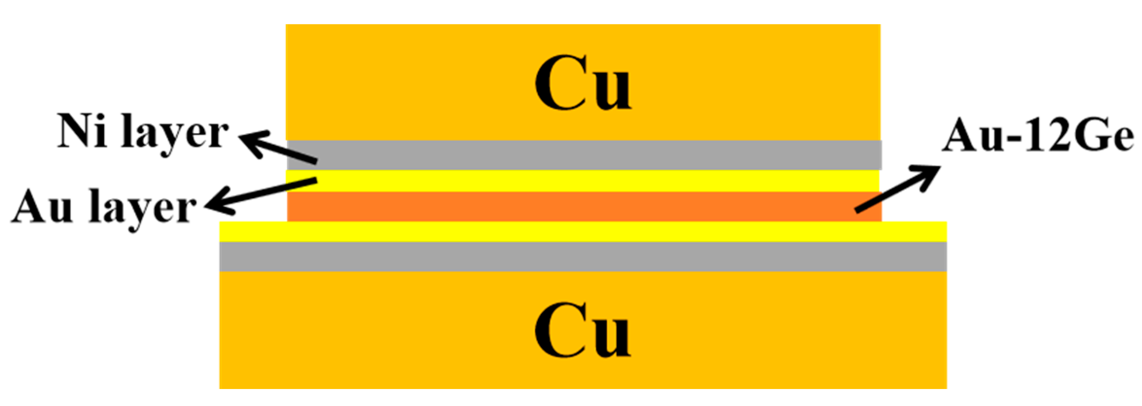
Bulk Au-12Ge eutectic thin films of a thickness of 25 μm and Cu sheets (4 mm × 4 mm × 1 mm, 20 mm × 10 mm × 1 mm) were prepared. In general, eutectic Au-Ge solder is usually used in systems with a metallization scheme based on the electroless nickel immersion gold (ENIG) system [23,24]. Therefore, the Cu sheets were metalized with a layer of 3.5 μm Ni diffusion barrier layer and 1.5 μm Au through integral electroplating. Selecting this substrate is owing to the Ni layer can prevent Au-12Ge from overreacting with the substrate. Simultaneously, the Au layer can effectively improve the wettability and restrain the oxidation corrosion to substrates. Prior to the soldering experiments, all the platelets were seriously cleaned with distilled water and ultrasonically rinsed in acetone and ethanol, and dried at room temperature. A small piece of Cu plate was placed on the larger plate. Au-12Ge (5 mm × 5 mm × 25 μm) solder alloy was soldered on both plates with the aid of no-clean 506 flux (NC506) to obtain the solder joint. The low eutectic point of Au-12Ge is at 12 wt.% Ge and 361 °C, as illustrated in Figure 1 [25]. Therefore, the soldering process was accomplished in a high-vacuum furnace (NBD-O1200, 10−3 Pa) at 410 °C for dwelling time of 2 min. Figure 2 shows the illustration of the overall structure of the joint.
Prepared samples were subjected to extreme thermal shock experiments to study the mechanical property and microstructure evolution of the solder and the solder joints under temperature variation. The low temperature was −196 °C, which was achieved by soaking the samples in the liquid nitrogen, while the high temperature was 150 °C, completed by placing the samples into the high-temperature cabinet. Both the high- and low-temperature storage time was 20 min. The entire process of thermal shock sustained for 400 cycles in which the microstructure observation was guided after every 100 cycles. All the cross-sections were from one joint, which could reduce the impact of other factors on the experiment and ensure the accuracy of this study.
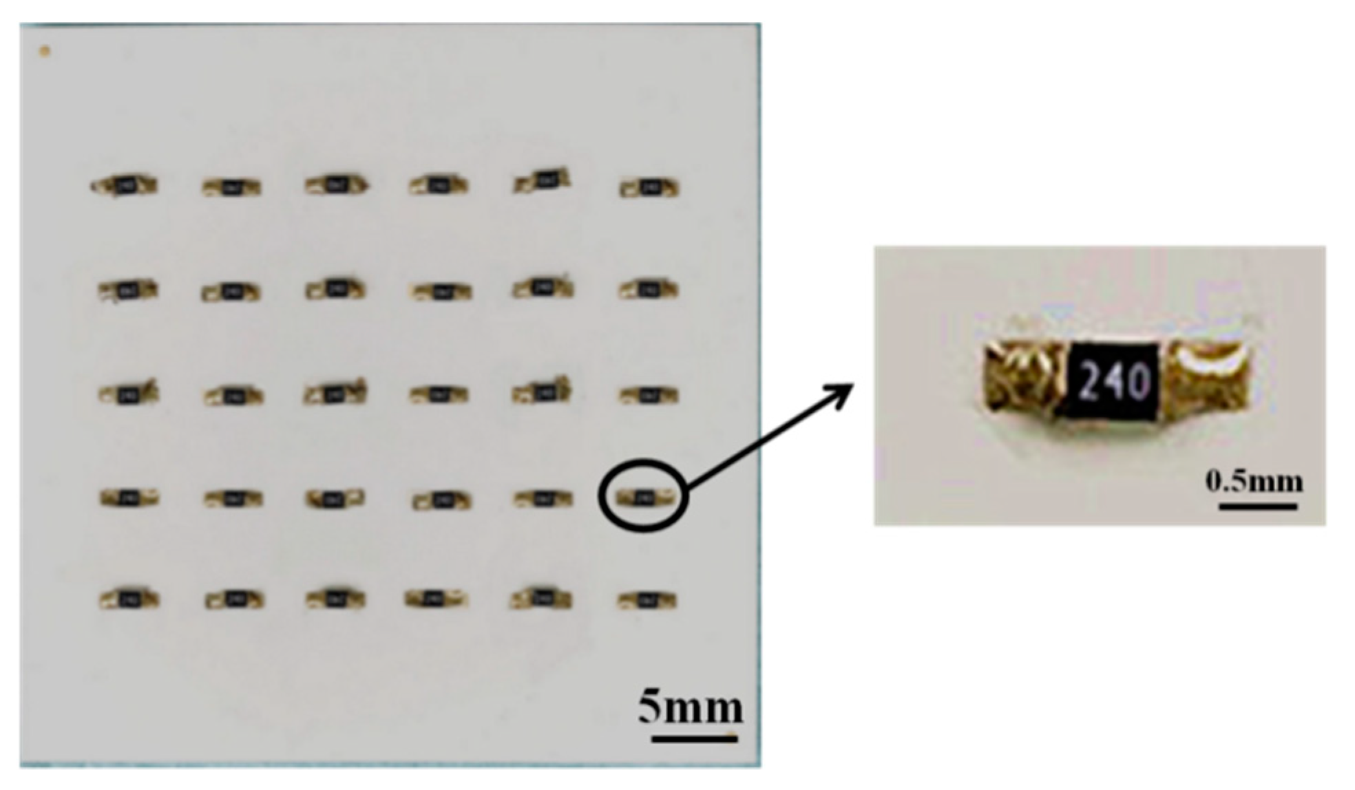
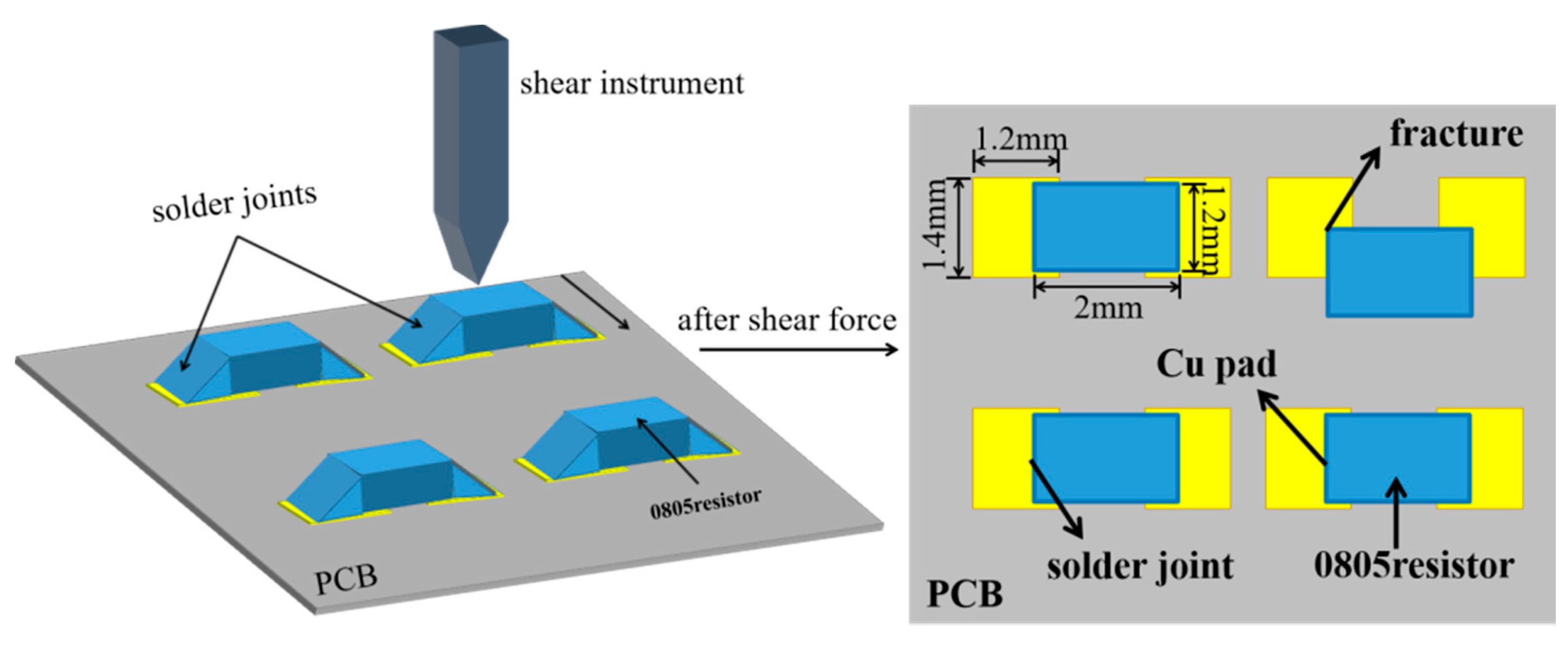
The as-produced and cycling joints were embedded, ground and polished by standard metallographic methods. Consequently, the microstructure observation of Au-12Ge solder was achieved by the metallographic microscope (DMILM, Leica, Somme, Germany). Moreover, the microstructure and fracture surface observation were achieved with the assistance of the scanning electron microscopy (SEM, Carl Zeiss, Jena, Germany). Meanwhile, the energy-dispersive spectrometer (EDS, Carl Zeiss, Jena, Germany) analysis was utilized to identify the compositions of the continuous intermetallic compound (IMC). Resistors were soldered onto the ceramic board by the studied solder to investigate the mechanical properties of the solder joints subjected to the aforementioned extreme cycling temperature. Both the Cu pads and resistors were metalized with Au and Ni layers, as shown in Figure 3. Afterwards, shear force tests were conducted by the STR-1000 joint strength tester (Rhesca Co., Ltd., Tokyo, Janpa), which can be seen in Figure 4. The shear strength was calculated by the formula: τ = Fmax/A, where τ is the shear strength (MPa), Fmax represents the maximum shear force (N) and A is the fracture surface area. Ten joints were tested under each parameter and their average value was calculated as the shear strength of the joints. Then, the morphology of the solder joint fracture was analyzed by SEM and EDS.
3. Results
3.1. The Microstructure Evolution of Au-12Ge Solder Joint during Extreme Thermal Shock
Figure 5 shows the microstructure of as-soldered/as reflowed Au-12Ge solder, which comprised of the bright Au phase and dark Ge phase dispersed in the former. As shown in Figure 1 and Table 1, at room temperature, the solubility of Au and Ge phases in each other was so low that it could be completely negligible. As a consequence, the Au and Ge phases existed as disparate phases.
The IMC layer, forming between Au-12Ge solder and the under-bump metallization (UBM) layer during the process of soldering, was highly essential to the reliability of the solder joint. As a rule, a uniform, thin and continuous IMC layer is a decisive factor for excellent metallurgical combination. However, the thick layer is brittle and prone to generate defects, which is very likely to degrade the joint reliability [26]. Even worse, if the substrate is over consumed, the IMC layer may spall. Therefore, the interfacial reactions of between Au-12Ge and Cu substrate as well as the interfacial microstructure evolution during extreme thermal shock have been studied.
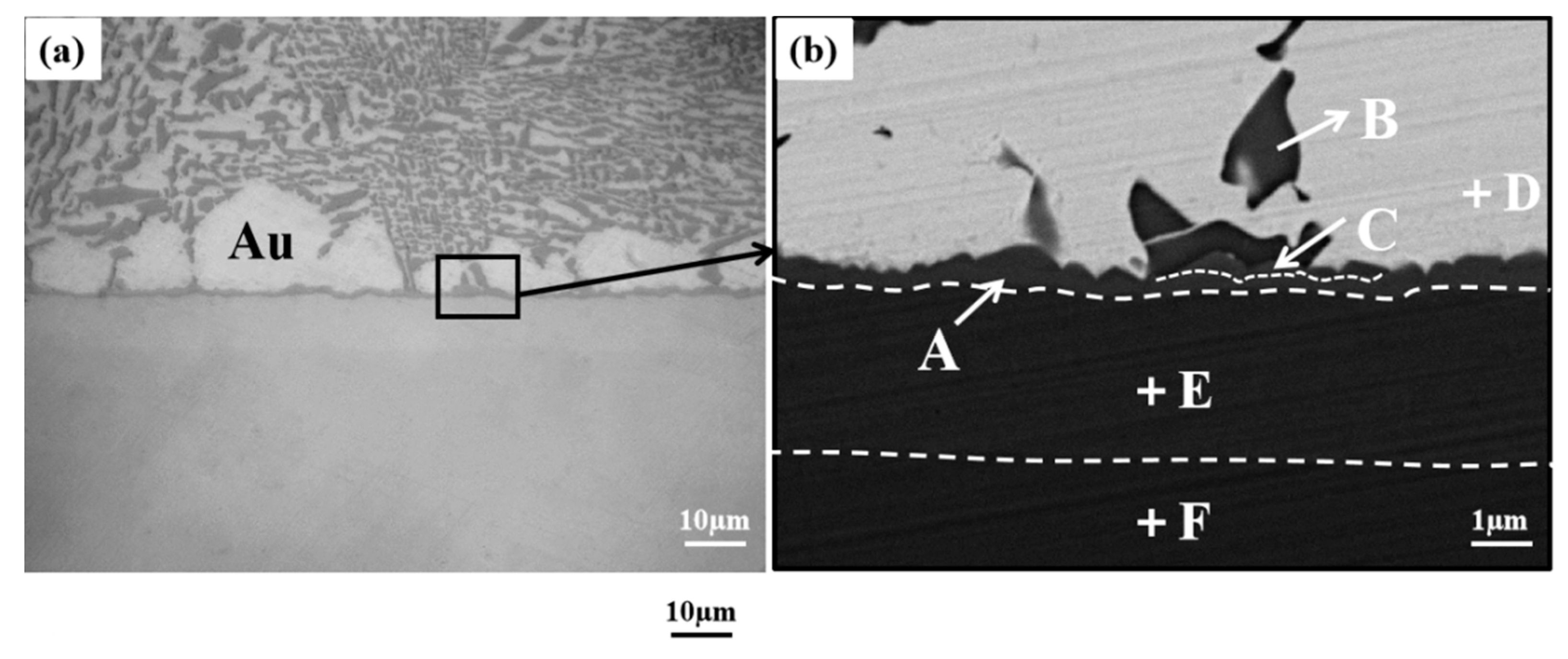
Figure 6 displayed the interfacial microstructure of Au-12Ge/Au/Ni/Cu solder joint after being soldered. The microstructure of the Au-12Ge solder near the interface layer was that the Ge phase dispersed uniformly in the bright Au phase, which can be seen from Figure 6a. Based on Figure 6b and the EDS analysis in Table 2, a continuous layer of Ni5Ge3 was detected at the interface of as-produced joint. There was also a continuous layer of NiGe phase with a scallop-like morphology adjacent to the Ni5Ge3 phase, which was similar to the research reported by Weyrich et al. [8,27,28]. There were no voids or other defects at the interface, which meant that the solder joint had complete structure. Interestingly, there was an almost pure gold zone near the IMC layer. This phenomenon may well be the reaction of Ge and the interconnection of Au. Meanwhile, the thickness of the IMC layer was relatively small due to the presence of Au layer. Therefore, merely a thin, uniform and continuous interface layer was formed.
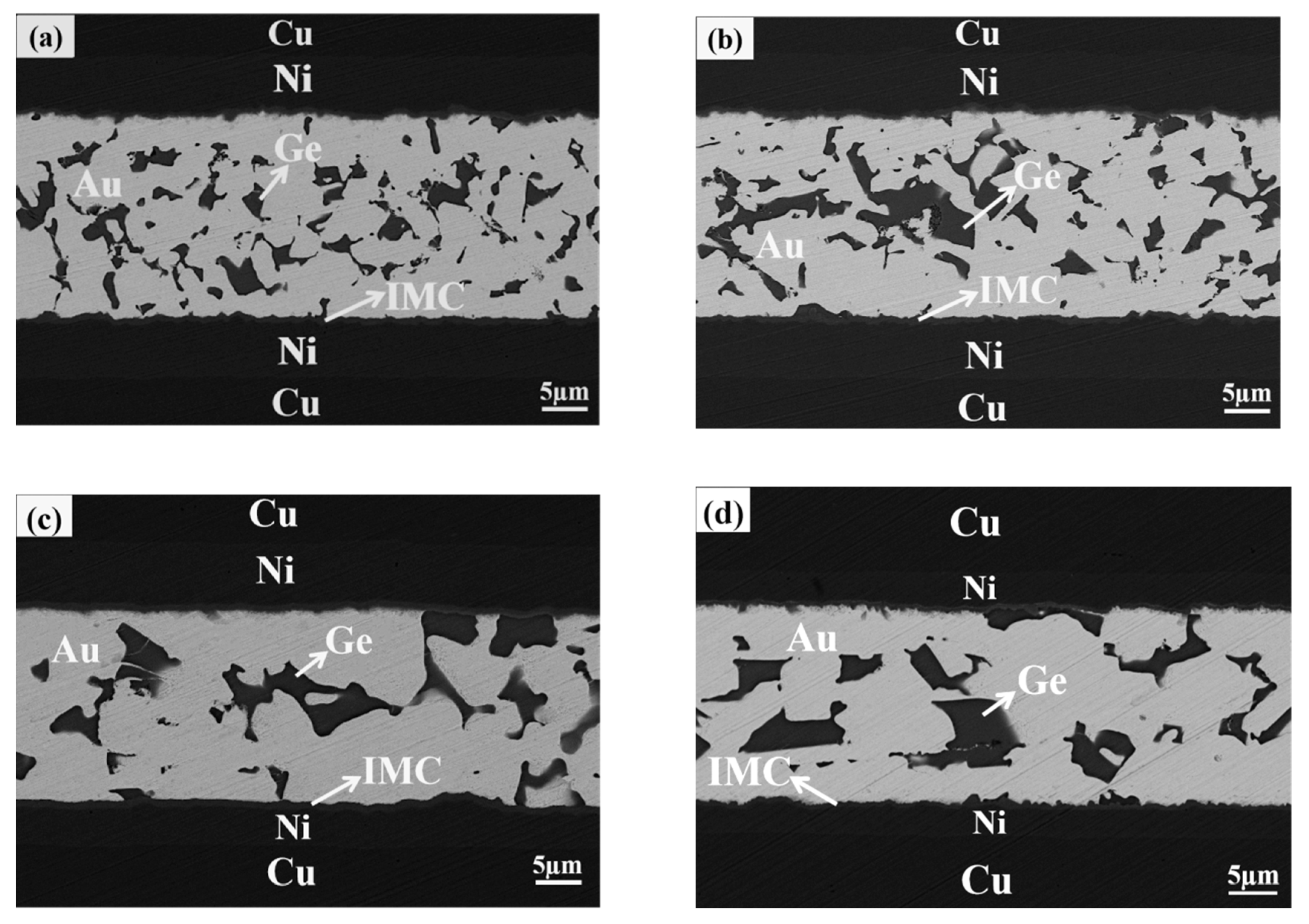
Figure 7 depicted the cross-sectional interfacial microstructure of Cu/Ni/Au/Au-12Ge/Au/Ni/Cu joints experienced the extreme thermal shock for different cycles. After thermal shock, the Au and Ge phase were also detached because of the low solubility of Au in Ge phase. After thermal shock for 100 cycles, the Ge phase was slightly coarsened as shown in Figure 7a. Coarsened Ge clustered together after 200 cycles, and fragmentized Ge was found as shown in Figure 7b. It cannot be seen clearly that the Au grains grew from the SEM images. Yet, the Au region interconnected well after 200 cycles due to the coarsen Ge, leading to the clustering of Ge phase and then a broader Au region. In fact, the coefficient of thermal expansion (CTE) of Au is 14.2 × 10⁻⁶/K, while that of Ge is 6.0 × 10⁻⁶/K. During extreme thermal shock, the CTE mismatch between Au and Ge phase may result in the internal strain of solder, and then deteriorate the mechanical property.
Besides, the interfacial morphologies were virtually the same when shocking for 100 and 200 cycles. The thickness of interface layer slightly increased, but not obvious. In a way, the slow growth rate of IMC was attributed to the low diffusion rate of Ni and Ge atoms. After 300 cycles, as depicted in Figure 7, the amount of Ge atoms adjacent to interface decreased dramatically. The Ge phase in Au-12Ge solder coarsened gradually and reacted with Ni to form Ni-Ge interfacial compounds, resulting in a deviation of eutectic structure. After 300 and 400 cycles, the morphology of the IMC layer changed from scallop-like type to planar type, which suggested that interfacial reaction occurred at the interface. It was worth mentioning that the interface layer was also thin even after 300 cycles.
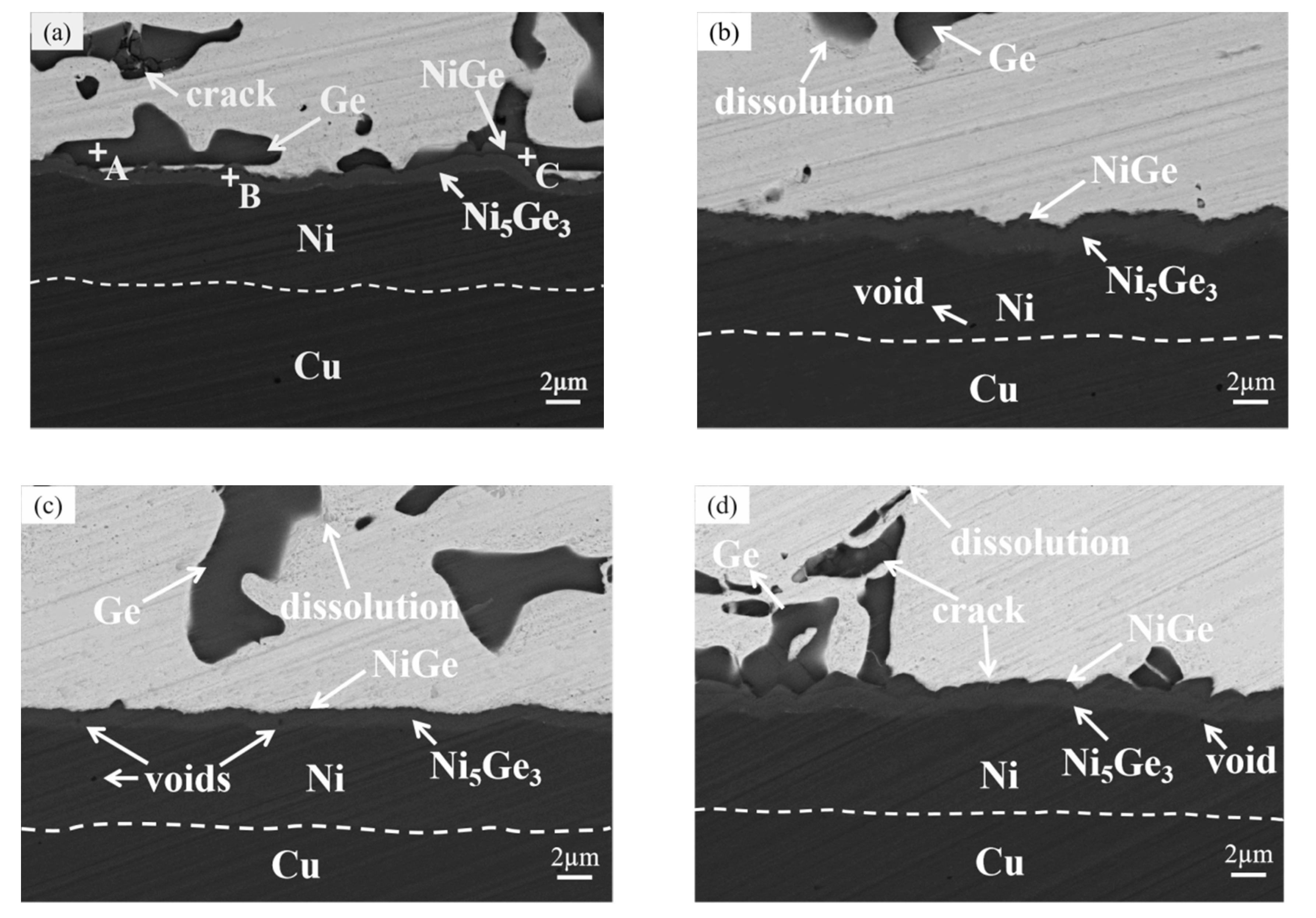
To analyze the interface reaction, the SEM image of magnifying interface layer was observed, which can be seen from Figure 8. After 200 cycles, the Ge phase dissolved slightly in Au phase, as can be seen from Figure 8b–d. As a result, the Au phase of Au-12Ge solder developed into (Au,Ge) solid-solution phase. Besides, the thickness of the IMC layer slightly increased during the test. As shown in Figure 8a and EDS analysis in Table 3, the NiGe layer of as-produced solder joint was thicker than that of Ni5Ge3 layer. At the beginning of cycling, the NiGe layer thinned, whereas the other layer got thicker. A small amount of Ni atoms passed through the Ni5Ge3 layer and reacted with NiGe through the reaction: 3NiGe + 2Ni = Ni5Ge3. It is worth stressing that the Ni5Ge3 phase was the most stable phase in Ni-Ge system from a thermodynamic point of view. As can be seen from Figure 8b,c, the NiGe layer was quite thin. Then, with the increasing of cycles, the influx of Ni atoms passed through the IMC layer, resulting in the rapid growth of the Ni5Ge3 phase. When the thickness of Ni5Ge3 layer reached a threshold, NiGe phase no longer converted to Ni5Ge3 phase and the NiGe layer was formed between the Ni5Ge3 layer and Au-12Ge solder, as can be seen from Figure 8d. Throughout the process, according to the Au-Ge binary diagram, the Ge solubility in the Au phase was very low, and Au phase hardly participated in the interface reaction. Ge atoms were consumed largely, while residual Ni atoms dissolved in Au phase.
As can also be seen from Figure 8a, a crack was found at the Ge phase, and a void was formed at the Cu layer. After 200 cycles, voids were found at both the Ni layer. Large voids and defects emerged in Ni5Ge3 IMCs layer after 300 cycles, as can be seen from Figure 8c. After 400 cycles, void and cracks were formed at both the Ge phase and NiGe layer. The Ge-Ni interface reaction was an atomic diffusion reaction, during where the diffusion rate of Ge and Ni atoms was different. There will be voids in the material with a slower diffusion rate, and then the voids will gradually accumulate to form the macroscopic voids and even cracks. It can be clearly seen that the cracks were formed when the voids in the IMC layer aggregated and extended from the interface layer to the solder matrix. The CTE mismatch between IMC and solder will also lead to defects mentioned above. During extreme thermal shock, the solder joint would experience rapidly cooling and heating in a large temperature variation. Thereinto, the CTE of Au-12Ge is 13.4 × 10⁻⁶/K, while that of NiGe, Ni5Ge3 and Ni are 10.1 × 10⁻⁶/K, 11.4 × 10⁻⁶/K and 14.1 × 10⁻⁶/K, respectively [29], and the CTE mismatch would then cause greater concentration of shear stress at the interfaces of IMC layer/ENIG UBM and solder/interfacial layer. The voids accumulation and cracks propagation would be the weakest area of the solder joint.
Beyond that, the formation of cracks between the IMC layer and Ni layer created a gap to prevent the further diffusion of Ni atoms, and thus lowered the growth velocity of interface layer.
3.2. Mechanical Properties of Au-12Ge Joints after Thermal Shock Test
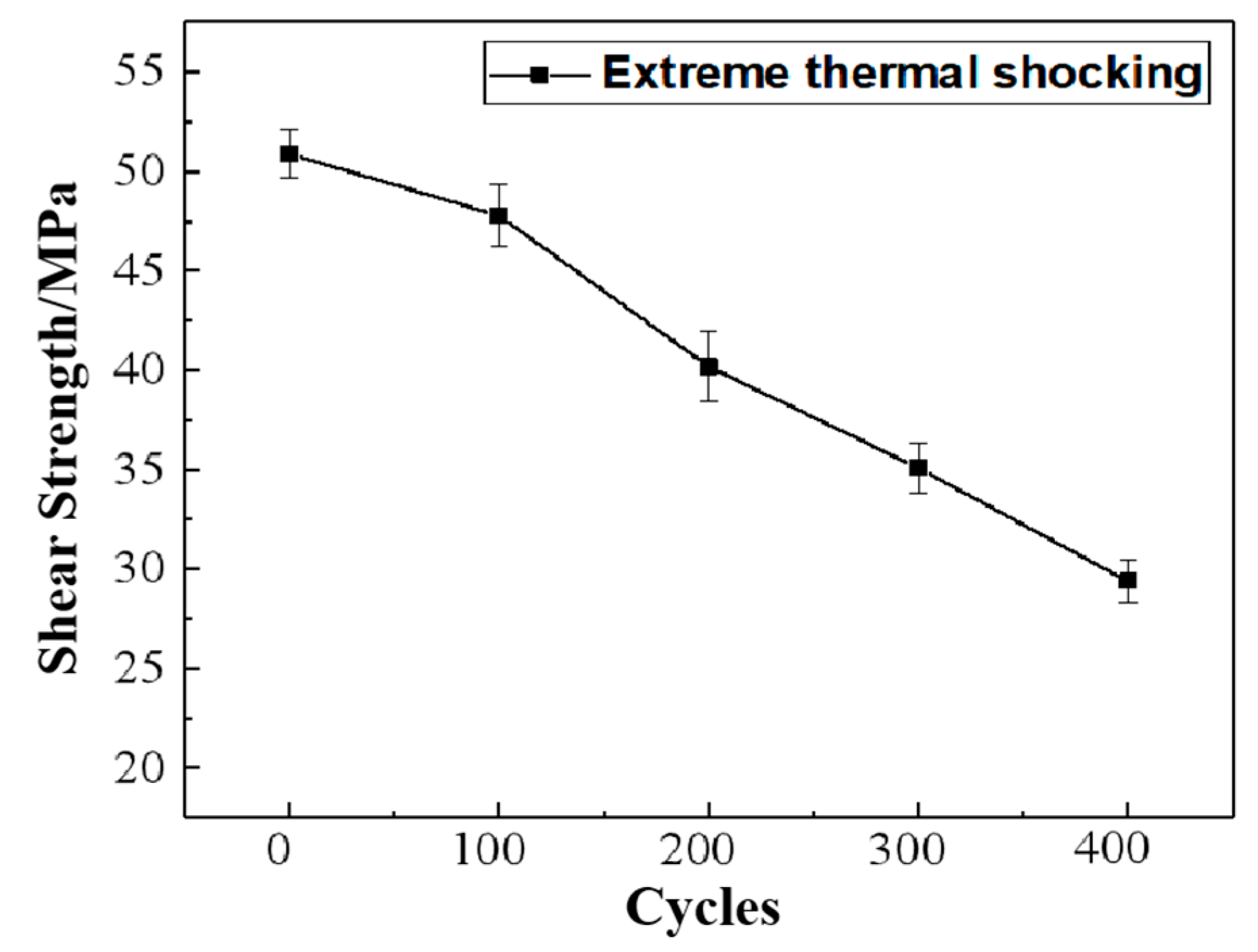
The shear tests were conducted to evaluate the effects of the different number of cycles on the mechanical properties of the solder joints. The result is shown in Figure 9; the strength of Cu/Ni/Au/Au-12Ge/Au/Ni/Cu solder joint reduced as the cycles increased. Before the test, the initial shear strength of the solder joint was 50.9 MPa, and the error value was 1.20 MPa. After 100 and 200 cycles, the shear strength of the solder joint was 47.8 and 40.2 MPa, and the error value was 1.56 and 1.74 MPa, respectively. After 300 cycles, the shear strength of the solder joint was 35.1 MPa, which deteriorated by 19.61%, and the error value was 1.24 MPa. After cycling for 400 periods, the graph revealed an obvious downtrend compared with the primordial shear strength, only 29.5 MPa, and the error value was 0.65 MPa. Thus, it can be seen that extreme thermal shock treatment played a negative role in the solder joint strength. Not only the thermal shock, but also the CTE mismatch between the solder and the IMC, would induce the formation and expansion of microscopic voids and micro-cracks. Generally speaking, both the micro-voids and micro-cracks will increase the risk of the joint fracture and then bring down the strength of the solder joint. Also, the formation of the brittle IMC layer may make the joint interface a relatively weak region, which was much more likely to degrade the joint strength.
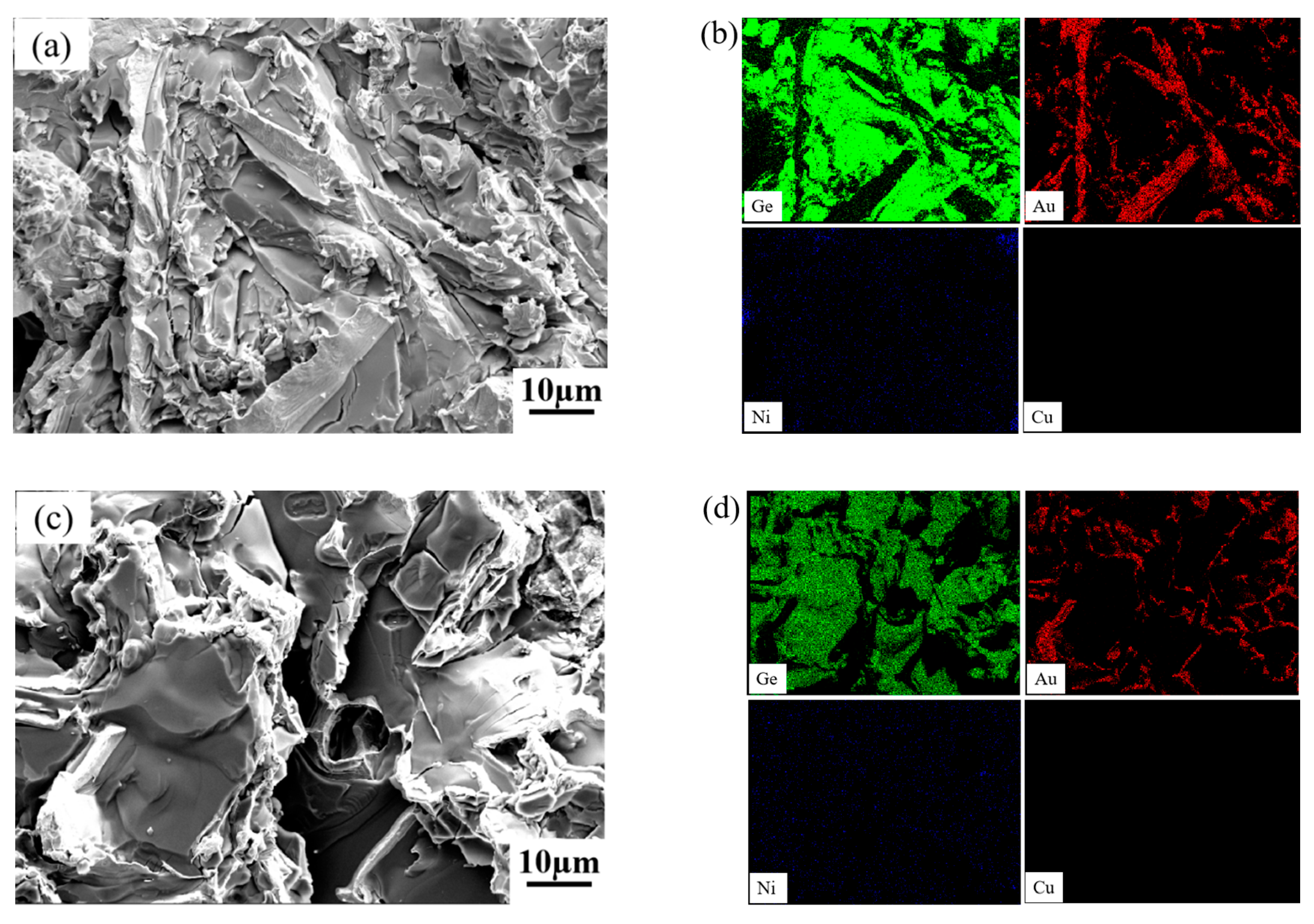
For the sake of investigating the fracture behavior of Cu/Ni/Au/Au-12Ge/Au/Ni/Cu joints after test, SEM and EDS analysis were conducted on the fracture of specimens subjected to different cycles after the shear test. Evidently, extreme thermal shock had a huge impact on the fracture morphology. As shown in Figure 10a, some dimples were found at the fracture surface, indicating that the fracture types were both the ductile and brittle mixed mode. Furthermore, the elemental mapping in Figure 10b exhibited a high-content Au and Ge element at the fracture, and the content of Ni and Cu element could be ignored, suggesting that the solder joint failed at the interior of Au-12Ge solder.
The joint after 100 cycles presented a similar fracture morphology with the joint not subjected to cycling. However, the Ge phase was obviously bulky than that of Figure 10a from the fracture surface, which is consistent with the microstructure observation in Figure 8a. Besides, the number of dimples decreased while the brittle fracture characteristics increased, still presenting a ductile-brittle fracture mode. Under this circumstance the shear strength lied on the solder. Bulky Ge phase and cracks inside the Ge phase would lead to the deterioration in the shear strength and transformation of fracture location and pattern. Therefore, the strength of solder would decline after 100 cycles, which would further decrease the shear strength.
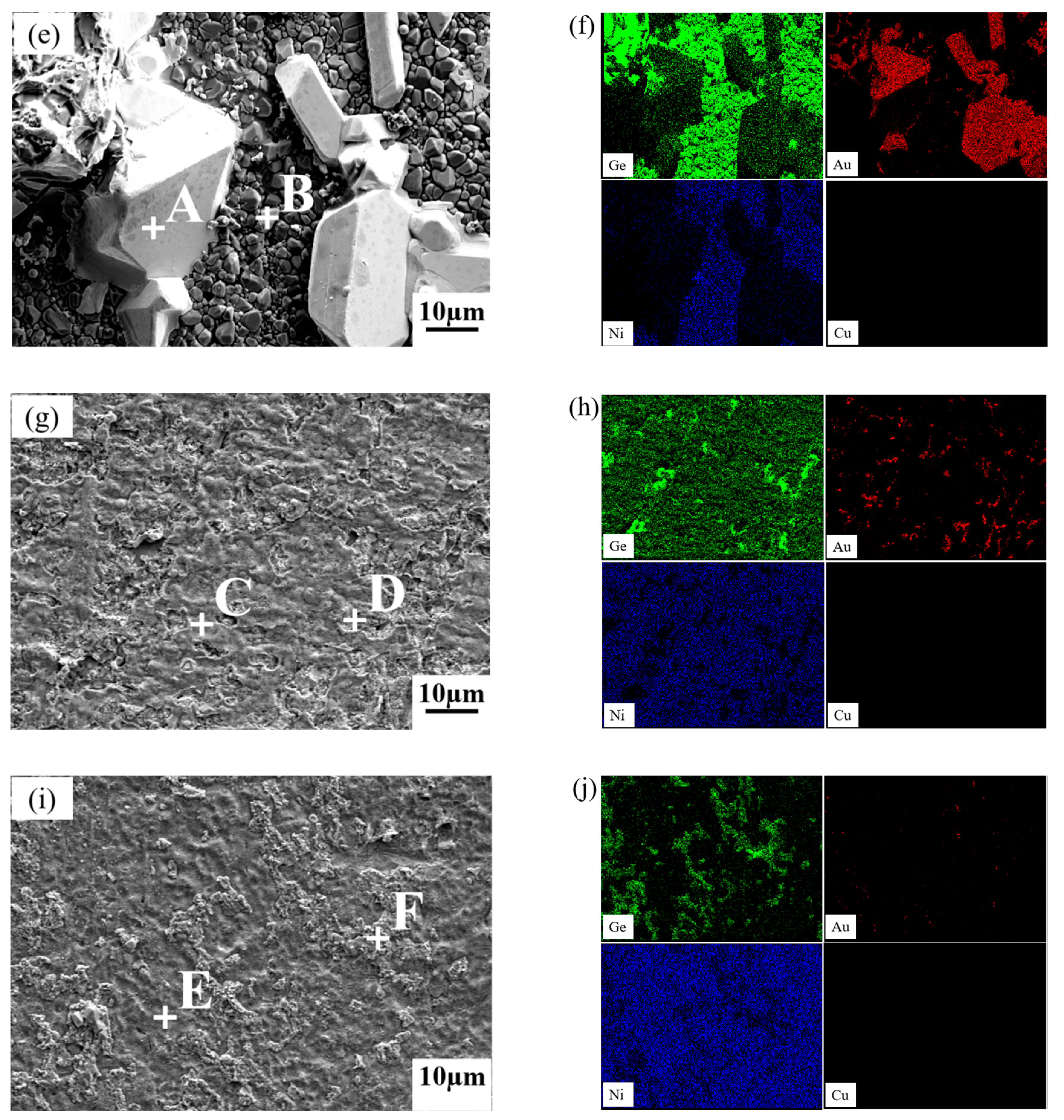
When the number of cycling was prolonged to 200, fine NiGe grains with rock-candy pattern and bulky Au phase were confirmed by the EDS analysis at the fracture surface, indicating that the crack propagated along the NiGe crystal of IMC layer and the near-interface Au-12Ge solder layer. During a large temperature variation, the difference of CTE may lead to inelastic energy or cyclic strain failure of Au-12Ge solder and IMC layer, which would lead to the reduction in the joint strength.
As depicted from Figure 10g, lane structure and several pits were found at the surface of the fracture. According to the elemental mapping and EDS analysis, the planar-patterned tissues were Ni5Ge3 phase, while the granular phases in the pit were NiGe compound. Some Ge phase was also detected from Figure 10h, which indicated that the fracture occurred in a mixed region of Ni, Ni5Ge3 phase and Au-12Ge solder. Both the shear stress concentration and cracks would make the shear strength decrease.
After 400 cycles, the surface demonstrated typical brittle characteristics in Figure 10i. As can be seen from Figure 10j, Ni was the essential element of the fracture, which signified that the granular-typed structure in Figure 10i was Ni layer. Meanwhile, the cluster-type Ni5Ge3 phase was detected by the element composition of points F in Table 4, which turned out that the fracture entirely happened at the interface between the IMC and Ni layer. It is worth pointing out that there were some voids on the fracture surfaces of the joints subjected to 300 and 400 cycles, which was easy to promote crack propagation. Consequently, the fatigue solder, concentration of stress and crack propagation would generate the deterioration of shear strength with the increasing of cycling.
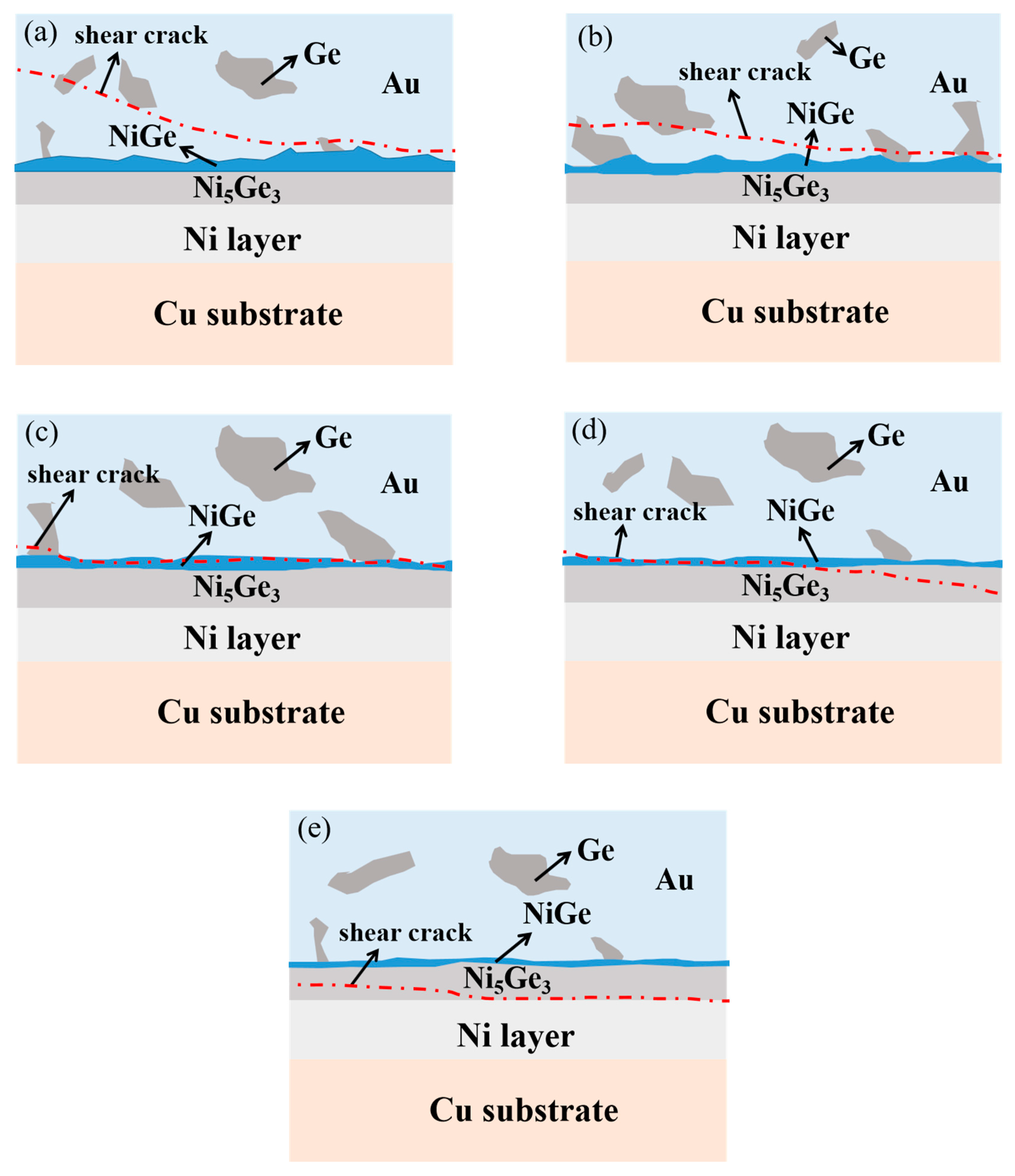
In summary, the fracture paths of solder joint experienced different cycles were summarized as shown in Figure 11. Fracture occurred in Au-12Ge solder matrix after 100 cycles. Cracks greatly affected the reliability of solder, which reduce the mechanical properties of solder joints. After 200 cycles, the fracture transformed from the solder/NiGe interface, NiGe/Ni5Ge3 interface into the interface of Ni5Ge3/Ni.
4. Conclusions
In this paper, the effect of extreme thermal shock on the microstructure evolution and mechanical properties of Cu/Ni/Au/Au-12Ge/Au/Ni/Cu joints as well as fracture behaviors/fracture mechanisms were investigated. The experiment results were summarized as follows:
- After soldering at 410 °C and dwelling for 2 min, the Cu/Ni/Au/Au-12Ge/Au/Ni/Cu joint was dense and faultless. The interface layer was uniform, thin and continuous. The IMCs from the Au-12Ge solder to the Cu basal plate were NiGe and Ni5Ge3, respectively.
- The extreme thermal shock had slight effects on the interfacial layer thickness of the joints. Even after 400 cycles, the IMC layer was quite thin. As the experiment went on, partial NiGe IMC layer converted into Ni5Ge3 IMC layer, resulting in a planar NiGe layer. After 100 cycles, cracks were formed at the Ge phase due to the fragile nature and higher hardness of Ge. Cracks were detected at Ni5Ge3, NiGe layer and Ge phase after 400 cycles. The stress concentration caused by the superior temperature variation and the mismatch CTE of solder, interface layer and substrate led to formation and propagation of cracks.
- The solder joint after soldering was 50.9 MPa. The shear strength of solder joints subjected to thermal shock was in a minor degradation due to the generation of defects. The strengths were 47.8 MPa after 100 cycles, 40.2 MPa after 200 cycles, 35.1 MPa after 300 cycles, 29.5 MPa after 400 cycles, respectively. The fracture shifted from solder to the solder/NiGe interface and then to the IMC layer with the increasing number of cycles. The fracture mode transformed from ductile-brittle type to the brittle type.
This study is beneficial to deeply understand the reliability of Au-12Ge solder joint in extreme temperature change. It can simultaneously provide a reference for the manufacture and packaging of electronic components in artificial satellites and spacecraft in future.
Author Contributions
Data curation, Z.W.; formal analysis, Z.W.; funding acquisition, S.X.; investigation, J.W.; methodology, Z.W.; project administration, S.X. and W.L.; software, Z.W.; supervision, S.X.; writing—original draft, Z.W.; writing—review and editing, Z.W., S.X., B.W. and P.Z. All authors have read and agreed to the published version of the manuscript.
Funding
This project was supported by the National Natural Science Foundation of China (Grant No. 51675269), the State Key Laboratory of Advanced Brazing Filler Metals & Technology (Zhengzhou Research Institute of Mechanical Engineering Co., Ltd.), China (Grant No. SKLABFMT201704) and the Priority Academic Program Development of Jiangsu Higher Education Institutions (PAPD).
Acknowledgments
The authors sincerely thank Songbai Xue for his critical discussion and reading during manuscript preparation.
Conflicts of Interest
The authors declare no conflict of interest.
References
- Jiang, N.; Zhang, L.; Liu, Z.Q.; Sun, L.; Long, W.M.; He, P.; Xiong, M.Y.; Zhao, M. Reliability issues of lead-free solder joints in electronic devices. Sci. Technol. Adv. Mater. 2019, 20, 876–901. [Google Scholar] [CrossRef] [PubMed] [Green Version]
- Tan, S.H.; Han, J.; Guo, F. Recrystallization Behavior in Mixed Solder Joints of BGA Components during Thermal Shock. J. Electron. Mater. 2018, 47, 4156–4164. [Google Scholar] [CrossRef]
- Wang, J.H.; Xue, S.B.; Lv, Z.P.; Wen, L.; Liu, S.Y. Study on the Reliability of Sn50Pb49Sb1/Cu Solder Joints Subjected to γ-ray Irradiation. Appl. Sci. 2018, 8, 1706. [Google Scholar] [CrossRef] [Green Version]
- Abtew, M.; Selvaduray, G. Lead-free Solders in Microelectronics. Mater. Sci. Eng. R-Rep. 2000, 27, 95–141. [Google Scholar] [CrossRef]
- Wu, J.; Xue, S.B.; Wang, J.W.; Xue, P. Effect of Thermal Cycling on Interfacial Microstructure and Mechanical Properties of Sn-0.3Ag-0.7Cu-(α-Al2O3) Nanoparticles/Cu Low-Ag Solder Joints. J. Electron. Mater. 2019, 48, 4562–4572. [Google Scholar] [CrossRef]
- Liu, S.F.; Zhang, D.X.; Xiong, J.R.; Chen, C.; Song, T.J.; Liu, L.; Huang, S.Y. Microstructure evolution and properties of rapidly solidified Au-20Sn eutectic solder prepared by single-roll technology. J. Alloys Compd. 2019, 4781, 873–882. [Google Scholar] [CrossRef]
- Chidambaram, V.; Hald, J.; Hattel, J. Development of Au-Ge based candidate alloys as an alternative to high-lead content solders. J. Alloys Compd. 2010, 490, 170–179. [Google Scholar] [CrossRef]
- Huang, Y.F.; Chen, X.; Xue, F.; Wu, T.; Liu, W.H.; Ma, Y.Z.; Tang, S.W. Effects of isothermal aging on interfacial microstructure evolution and shear behavior of Au-12Ge/Ni(P)/Cu Solder Joints. Intermetallics 2020, 124, 106865. [Google Scholar] [CrossRef]
- Wen, L.; Xue, S.B.; Wang, L.J.; Liu, H.; Wu, J. Microstructural evolution and shear performance of AuSn20 solder joint under gamma-ray irradiation and thermal cycling. J. Mater. Sci. Mater. Electron. 2020, 31, 7200–7210. [Google Scholar] [CrossRef]
- Li, J.Z.; Acoff, V.L.; Gong, X.B. Characterization of the brittle mechanism in a Au-Ge microalloy. Gold Bull. 2015, 48, 47–56. [Google Scholar] [CrossRef] [Green Version]
- Zeng, G.; Mcdonald, S.; Nogita, K. Development of high-temperature solders: Review. Microelectron. Reliab. 2012, 52, 1306–1322. [Google Scholar] [CrossRef]
- Chidambaram, V.; Yeung, H.B.; Shan, G. Reliability of Au-Ge and Au-Si Eutectic Solder Alloys for High-Temperature Electronics. J. Electron. Mater. 2012, 41, 2107–2117. [Google Scholar] [CrossRef]
- Lau, F.L.; Made, R.I.; Putra, W.N.; Lim, J.Z.; Nachiappan, V.C.; Aw, J.L.; Gan, C.L. Electrical behavior of Au-Ge eutectic solder under aging for solder bump application in high temperature Electronics. Microelectron. Reliab. 2013, 53, 1582–1586. [Google Scholar] [CrossRef]
- Zhang, Y.M.; Zhu, H.L.; Fujiwara, M.; Xu, J.Q.; Dao, M. Low-temperature creep of SnPb and SnAgCu solder alloys and reliability prediction in electronic packaging modules. Scr. Mater. 2013, 68, 607–610. [Google Scholar] [CrossRef]
- Wang, J.H.; Xue, S.B.; Lv, Z.P.; Wen, L.; Liu, S.Y. Microstructure and performance evolution of SnPbSb solder joint under γ-ray irradiation and thermal cycling. J. Mater. Sci. Mater. Electron. 2019, 30, 1–10. [Google Scholar] [CrossRef]
- Wang, J.; Leinenbach, C.; Roth, M. Thermodynamic modeling of the Au–Ge–Sn ternary system. J. Alloys Compd. 2009, 481, 830–836. [Google Scholar] [CrossRef]
- Zhao, L.Y.; Tian, Y.H.; Tian, R.Y.; Wang, C.X. Mechanical properties and fracture mechanisms of Sn-3.0Ag-0.5Cu solder alloys and joints at cryogenic temperatures. Mater. Sci. Eng. A 2017, 684, 697–705. [Google Scholar]
- Tian, R.Y.; Hang, C.J.; Tian, Y.H.; Zhao, L.Y. Growth behavior of intermetallic compounds and early formation of cracks in Sn-3Ag-0.5Cu solder joints under extreme temperature thermal shock. Mater. Sci. Eng. A 2017, 709, 125–133. [Google Scholar] [CrossRef]
- Drevin-Bazin, A.; Badawi, F.; Lacroix, F.; Barbot, J.F. Investigation of Die Attach for SiC Power Device for 300 °C Applications. Mater. Sci. Forum 2013, 742, 1032–1035. [Google Scholar] [CrossRef]
- Jin, S.; Valenza, F.; Novakovic, R.; Leinenbach, C. Wetting Behavior of Ternary Au-Ge-X (X=Sb, Sn) Alloys on Cu and Ni. J. Electron. Mater. 2013, 42, 1024–1032. [Google Scholar] [CrossRef] [Green Version]
- Ma, Y.Z.; Wu, T.; Liu, W.S.; Huang, Y.F.; Tang, S.W.; Wang, Y.K. Interfacial microstructure evolution and shear behavior of Au-12Ge/Ni solder joints during isothermal aging. J. Mater. Sci.-Mater. Electron. 2017, 28, 3685–3694. [Google Scholar] [CrossRef]
- Dong, H.Q.; Vuorinen, V.; Liu, X.W.; Laurila, T.; Krockel, M.P. Microstructural Evolution and Mechanical Properties of Au-20wt.%Sn/Ni Interconnection. J. Electron. Mater. 2015, 45, 566–575. [Google Scholar] [CrossRef]
- Leinenbach, C.; Valenza, F.; Giuranno, D.; Elsener, H.R.; Novakovic, S.J.R. Wetting and Soldering Behavior of Eutectic Au-Ge Alloy on Cu and Ni Substrates. J. Electron. Mater. 2011, 40, 1533–1541. [Google Scholar] [CrossRef] [Green Version]
- Lang, F.Q.; Yamaguchi, H.; Nakagawa, H.; Sato, H. Solid-State Interfacial Reaction between Eutectic Au−Ge Solder and Cu/Ni(P)/Au Metalized Ceramic Substrate and Its Suppression. J. Mater. Sci. Technol. 2015, 31, 445–452. [Google Scholar] [CrossRef]
- Weyrich, N.; Jin, S.; Duarte, L.I.; Leinenbach, C. Joining of Cu, Ni, and Ti Using Au-Ge-Based High-Temperature Solder Alloys. J. Mater. Eng. Perform. 2014, 23, 1585–1592. [Google Scholar] [CrossRef] [Green Version]
- Lin, S.K.; Tsai, M.Y.; Tsai, P.C.; Hsu, B.H. Formation of alternating interfacial layers in Au-12Ge/Ni joints. Sci. Rep. 2015, 4, 4557. [Google Scholar] [CrossRef] [Green Version]
- Jin, S.; Leinenbach, C.; Wang, J.; Duarte, L.I.; Delsante, S.; Borzone, B.; Scott, A.; Watson, A. Thermodynamic study and reassessment of the Ge-Ni system. Calphad 2012, 38, 23–34. [Google Scholar] [CrossRef]
- Weyrich, N.; Leinenbach, C. Characterization of the isothermal solidification process in the Ni/Au-Ge layer system. J. Mater. Sci. 2015, 50, 3835–3844. [Google Scholar] [CrossRef]
- Weyrich, N.P. Joining of Metals and Ceramics Using Au-(Ge, Si)-Based Solder Alloys. Ph.D. Thesis, ETH Zürich, Zürich, Switzerland, 2015. [Google Scholar]
Figure 1.
Phase diagram of Au-Ge alloy [25] (with permission from Spring Nature, 2020).
Figure 1.
Phase diagram of Au-Ge alloy [25] (with permission from Spring Nature, 2020).

Figure 2.
The schematic diagram of Cu/Ni/Au/Au-12Ge/Au/Ni/Cu joint.

Figure 3.
Top view of the micro-joints on Al2O3 substrate.

Figure 4.
The diagram of shear test.

Figure 5.
Optical microstructure of Au-12Ge solder.

Figure 6.
Scanning electron microscopy (SEM) micrograph of Au-12Ge/Cu interface after soldering: (a) 1000×; (b) 5000×.
Figure 6.
Scanning electron microscopy (SEM) micrograph of Au-12Ge/Cu interface after soldering: (a) 1000×; (b) 5000×.

Figure 7.
SEM micrograph of Cu/Ni/Au/Au-12Ge/Au/Ni/Cu solder joints: (a) 100 cycles; (b) 200 cycles; (c) 300 cycles; (d) 400 cycles.
Figure 7.
SEM micrograph of Cu/Ni/Au/Au-12Ge/Au/Ni/Cu solder joints: (a) 100 cycles; (b) 200 cycles; (c) 300 cycles; (d) 400 cycles.

Figure 8.
The SEM image of Cu/Ni/Au/Au-12Ge/Au/Ni/Cu interfacial layer: (a) 100 cycles; (b) 200 cycles; (c) 300 cycles; (d) 400 cycles.
Figure 8.
The SEM image of Cu/Ni/Au/Au-12Ge/Au/Ni/Cu interfacial layer: (a) 100 cycles; (b) 200 cycles; (c) 300 cycles; (d) 400 cycles.

Figure 9.
The shear strength of Au-12Ge solder joint during thermal shock.

Figure 10.
The fracture surfaces of solder joints: (a) as soldered; (b) elemental mapping of (a); (c) after 100 cycles; (d) elemental mapping of (c); (e) after 200 cycles; (f) elemental mapping of (e); (g) after 300 cycles; (h) elemental mapping of (g); (i) after 400 cycles; (j) elemental mapping of (i).


Figure 11.
The schematic illustration of shear failures in Au-12Ge/Au/Ni/Cu joints after shock: (a) 0 cycle; (b) 100 cycles; (c) 200 cycles; (d) 300 cycles; (e) 400 cycles.
Figure 11.
The schematic illustration of shear failures in Au-12Ge/Au/Ni/Cu joints after shock: (a) 0 cycle; (b) 100 cycles; (c) 200 cycles; (d) 300 cycles; (e) 400 cycles.


Table 1.
The energy-dispersive spectrometer (EDS) results of Figure 5.
Table 1.
The energy-dispersive spectrometer (EDS) results of Figure 5.
| Points | Composition, at.% | Phase | |
|---|---|---|---|
| Au | Ge | ||
| A | 98.32 | 1.68 | Au |
| B | 0 | 100.00 | Ge |
Table 2.
The EDS results of Figure 6.
Table 2.
The EDS results of Figure 6.
| Points | Composition, at.% | Phase | |||
|---|---|---|---|---|---|
| Au | Ge | Ni | Cu | ||
| A | - | 38.72 | 61.28 | - | Ni5Ge3 |
| B | - | 100.00 | - | - | Ge |
| C | - | 49.31 | 50.69 | - | NiGe |
| D | 100.00 | - | - | - | Au |
| E | - | - | 100.00 | - | Ni |
| F | - | - | - | 100.00 | Cu |
Table 3.
The EDS results of Figure 8a.
Table 3.
The EDS results of Figure 8a.
| Points | Composition, at.% | Phase | ||
|---|---|---|---|---|
| Au | Ge | Ni | ||
| A | - | 100.00 | - | Ge |
| B | - | 38.33 | 61.67 | Ni5Ge3 |
| C | 0.30 | 50.63 | 49.07 | NiGe |
Table 4.
The EDS results of Figure 10.
Table 4.
The EDS results of Figure 10.
| Points | Composition, at.% | Phase | ||
|---|---|---|---|---|
| Au | Ge | Ni | ||
| A | 88.58 | 7.96 | 3.46 | Au |
| B | 0.60 | 51.53 | 47.87 | NiGe |
| C | - | 38.63 | 61.37 | Ni5Ge3 |
| D | 1.83 | 47.51 | 50.67 | NiGe |
| E | - | - | 100.00 | Ni |
| F | - | 39.12 | 62.88 | Ni5Ge3 |
Publisher’s Note: MDPI stays neutral with regard to jurisdictional claims in published maps and institutional affiliations. |
© 2020 by the authors. Licensee MDPI, Basel, Switzerland. This article is an open access article distributed under the terms and conditions of the Creative Commons Attribution (CC BY) license (http://creativecommons.org/licenses/by/4.0/).
Share and Cite
MDPI and ACS Style
Wang, Z.; Xue, S.; Long, W.; Wang, B.; Wang, J.; Zhang, P. Effects of Extreme Thermal Shock on Microstructure and Mechanical Properties of Au-12Ge/Au/Ni/Cu Solder Joint. Metals 2020, 10, 1373. https://doi.org/10.3390/met10101373
AMA Style
Wang Z, Xue S, Long W, Wang B, Wang J, Zhang P. Effects of Extreme Thermal Shock on Microstructure and Mechanical Properties of Au-12Ge/Au/Ni/Cu Solder Joint. Metals. 2020; 10(10):1373. https://doi.org/10.3390/met10101373
Chicago/Turabian StyleWang, Ziyi, Songbai Xue, Weimin Long, Bo Wang, Jianhao Wang, and Peng Zhang. 2020. "Effects of Extreme Thermal Shock on Microstructure and Mechanical Properties of Au-12Ge/Au/Ni/Cu Solder Joint" Metals 10, no. 10: 1373. https://doi.org/10.3390/met10101373
Note that from the first issue of 2016, this journal uses article numbers instead of page numbers. See further details here.