

Abstract
The concept of a cryogenic low-noise amplifier (LNA) using quantized conduction in a 1D channel is proposed and explored through simulations. A MOSFET with a 1D channel (nanowire) will exhibit the formation of plateaus in the current due to sub-band quantization at temperatures of below about 100 K and low drive bias. Using a ballistic 1D top-of-the-barrier model, we show that the current plateaus significantly enhance the transconductance, enabling low noise and high gain at low DC power dissipation—key characteristics for LNA applications such as quantum computing. The results indicate that cryogenic 1D ballistic MOSFETs may offer a significant improvement in noise performance and power dissipation (40x reduction) over traditional devices for cryogenic applications with low input power, such as quantum computing.
Export citation and abstract BibTeX RIS
1. Introduction
Low-noise amplifiers (LNAs) operating under cryogenically cooled conditions, typically below 15 K [1, 2], have found a number of important applications. LNAs are intentionally cooled in order to improve noise performance, which is dependent on electron transport properties and thermal noise in parasitic elements. This is useful in e.g. space applications, such as space communication and astronomy [3, 4]. The temperature of an antenna pointed to outer space is the background temperature of 2.7 K, which is dominated by the receiver noise temperature, unless cryogenically cooled. A second class of applications are high-sensitivity measurements at cryogenic conditions, such as superconductor physics and quantum computing, in which LNAs often must be co-integrated with test structures inside the cryostat [5]. In these cases, a main concern is the power dissipation of the LNA, limited by the cooling system's ability to remove generated heat. In particular, quantum computing applications may in the future require integration of electronics at sub-Kelvin stages in the cryostat, where cooling power is a few hundreds of micro-Watts or lower [5]. Even at higher temperature stages, such as 3 or 4 K, where several Watts of cooling power is available, power budget management will be crucial for dense quantum systems with highly parallelized qubit readout.
State-of-the-art LNAs optimized for cryogenic conditions use InAs/InP high electron mobility transistors (HEMTs) [6], and target a low minimum noise temperature Tmin , empirically described as [4]
where Rt = Ri + Rs + Rg, Ri is the intrinsic gate to source resistance, and Rs and Rg are the parasitic source and gate resistances. Tg and Td are the equivalent temperatures of the gate and the channel respectively. Gd is the output conductance of the device. To minimize Tmin, the ratio gm /√IDS , the transconductance over the square root of the drain current, must be maximized, which is typically done by tuning the bias point of the transistor. Though state-of-the-art devices obtain Tmin of 1.4 K at ambient temperature of 5 K, power dissipation PDC is in the order of several milli-watt [6]. PDC determines at what minimum temperature stage in the cryostat the LNA can be operated, i.e. the 3 or 4 K stages for present technology.
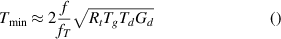
In this work, we propose a new type of cryogenic amplifier, a 1D-LNA, which utilizes the properties of a quasi-ballistic MOSFET implementing a 1D (nanowire) channel [7]. Figure 1(a) illustrates an example of this type of device with three parallel lateral nanowires, though it could also be implemented in the vertical direction using vertical nanowires [8]. Such a device will exhibit current steps in the transfer characteristics at cryogenic conditions (also known as quantized conductance) [9, 10]. An amplifier operating at the edge of the first current step exhibits large transconductance and low drain current at a low VDS of 10–50 mV and provides a strong reduction of DC power dissipation. The characteristics of the 1D-LNA are here determined by simulation using an analytical quasi-ballistic 1D top-of-the-barrier model and small-signal modeling.
Figure 1. (a) Schematic of MOSFET with three parallel nanowires. (b) Drain currents for one nanowire at 10 mV drive bias and temperatures 30 and 300 K, illustrating quantized conductance at 30 K. (c) Transconductance, gm , peak shape at different temperatures. At lower temperatures, the maximum gm increases, while the peak width narrows. (d) gm versus temperature and drive bias, showing that at very low temperatures, gm decouples from VDS and reaches its maximum value independent of VDS down to about 10 mV.
Download figure:
Standard image High-resolution image2. Simulations
The top-of-the-barrier model describes the operation of a 1D quasi-ballistic transistor by carrier transport between two ideal electron reservoirs, source and drain, through a channel region with one or several conducting sub-bands [7]. The current between the reservoirs is  . The forward current is

where  is the Fermi–Dirac integral of the nth order, and
  = (EF
—
= (EF
— (0))/kBTL
is the normalized Fermi energy. TL
is the lattice temperature. For the reverse current
(0))/kBTL
is the normalized Fermi energy. TL
is the lattice temperature. For the reverse current  the Fermi energy is lowered due to the applied drive voltage VDS
by
the Fermi energy is lowered due to the applied drive voltage VDS
by  . Assuming ideal electrostatics, the energy at the top of the barrier, i.e. the bottom of the first sub-band in the channel, is described as
where nL
is the carrier density and COX
is the oxide capacitance. (0) is calculated self-consistently from
[11, 12]. The drain current is subsequently described as
where T is the transmission, a transport parameter dependent on the mobility and gate length of the device [13].
Using equations (1)–(3), IDS
can be calculated in a self-consistent manner. The Fermi energy EF
is calculated by solving the Schrödinger equation for a 1D structure. This confinement of the electron wave function in a nanowire results in quantization of the conduction and valence bands into multiple sub-bands. At low temperatures quantized conduction emerges for each energy sub-band, due to the increasing sharpness of the Fermi distribution function [14]. Each sub-band n will contribute to the current as  . Figure 1(b) shows the IDS
and gm
for a device with three sub-bands at 30 K and 300 K. In0.53Ga0.47As is chosen for the channel material due to the larger Bohr radius compared to Si, which facilitates energy quantization at larger nanowire diameter [15]. The transconductance gm
is independent of the current level at 30 K, as each peak has the same maximum value. The optimal operation point of the proposed 1D-LNA is at a DC gate voltage of the first gm
peak where gm
/√IDS
is maximized. We note that the quantum capacitance CQ is a result of equation (2), since it is a complete expression of the channel charge density. Its effect is thus included in the calculation of IDS
[16].
. Figure 1(b) shows the IDS
and gm
for a device with three sub-bands at 30 K and 300 K. In0.53Ga0.47As is chosen for the channel material due to the larger Bohr radius compared to Si, which facilitates energy quantization at larger nanowire diameter [15]. The transconductance gm
is independent of the current level at 30 K, as each peak has the same maximum value. The optimal operation point of the proposed 1D-LNA is at a DC gate voltage of the first gm
peak where gm
/√IDS
is maximized. We note that the quantum capacitance CQ is a result of equation (2), since it is a complete expression of the channel charge density. Its effect is thus included in the calculation of IDS
[16].
Several non-ideal effects are expected. (i) Transmission will be smaller than one, hence quasi-ballistic transport. This will reduce the gain of the transistor. In this work, we use a transmission T = 0.8 for all sub-bands, as has been reported for the InxGa1-xAs system [14]. One of the main causes of reduction of the transmission is likely interface defect scattering. (ii) Nanowire size variations will broaden the transconductance peaks and can be modeled as a higher effective temperature of operation. Hence, we chose a simulation temperature of 30 K (unless otherwise stated), while the target ambient temperature is 4 K or below, to more accurately depict expected experimental results. (iii) Line edge roughness will introduce a perturbation to the channel energy bands and can be modeled using atomistic tight binding models but is outside the scope of this work [17, 18]. In general, non-ideal effects will cause a less sharp cutoff of the transmission for energies below the subband edge. However, the increase of gm in this type of device does not entirely originate from a sharp cutoff but comes from the unique behavior of gm in a quantized system. Namely, gm = T2q2/h in the quantum capacitance limit, i.e. a decoupling of gm from VDS , as compared to a traditional FET.
3. Results
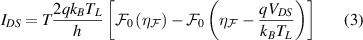
For the simulations, we use a cylindrical nanowire with a radius of 5 nm with the first sub-band at 0.2 V. We do not assume a value of the gate length LG , except that the transmission be T = λ/(λ + L) = 0.8. Figure 1(c) shows the gm peak shape at different temperatures at VDS = 10 mV. At lower temperatures, the maximum gm increases, while the peak width narrows. The maximum value saturates at T2q2/h at sufficiently low temperatures (note that T is the transmission), i.e. gm decouples from VDS . This is valid only in the quantum capacitance limit, where the oxide capacitance is much greater than the quantum capacitance. State-of-the-art MOSFETs with scaled gate oxides are expected to operate in this region. In the classical limit, gm is dependent on VGS , though not VDS . This effect is further explored in figure 1(d), showing maximum gm values versus temperature and VDS . At 10 mV, the decoupling temperature is about 10 K, while it increases for higher VDS . As can be seen, lower VDS leads to a stronger increase from room-temperature to low temperature. This gm enhancement, gm(TL)/gm (300 K) is shown in figure 2(a) versus temperature and VDS . The gm enhancement can be as large as 10.4 for temperatures below 10 K and VDS = 10 mV. This boost in gm is unique for the quantized transistor, since for conventional MOSFETs gm does not typically depend strongly on temperature, except for carrier mobility enhancement due to reduced phonon scattering, which tends to be modest. We note that gm enhancement in quantized FETs has been experimentally reported, e.g. in [9], showing a factor ∼3 boost at 11 K. We also note that while a complete decoupling of VDS from gm is predicted, it is not a necessary feature of the proposed device [19]. A reduction of the VDS dependence is functionality identical to a boost of gm at iso-VDS, which is the important aspect for low-power device operation.
The output conductance, gd , and the intrinsic voltage gain Av = gm /gd for the first sub-band at VDS = 10 mV and TL = 30 K are shown in figure 2(b). The voltage gain at the first gm peak is 10. At the current plateau, the current is IDS = TVDS 2q2 /h, thus the output conductance gd = dIDS /dVDS = T2q2 /h. This is the same value as gm , implying that voltage gain cannot be achieved. However, maximum gd is achieved when IDS has saturated at the plateau value, while maximum gm is achieved as IDS increases to the plateau value. Voltage gain is therefore possible and will depend on temperature and VDS . Note that gm and gd in figure 2(d) have different maximum values due to that 30 K is above the saturation temperature for VDS = 10 mV, which only impacts the gm value.
High-frequency characteristics are determined by use of a hybrid-π small signal model [20], as shown in figure 3(a). To obtain realistic simulation results, the values of the parasitic elements are taken from [21], which represents a device structure similar to what is needed to implement the proposed 1D-LNA, i.e. an InGaAs nanowire MOSFET with ∼300 parallel nanowires. We use 300 nanowires with 5 nm radius and 10 nm spacing, and with the parasitic capacitances from [20] normalized to the resulting total gate width. Figure 3(b) shows the associated gain values of the device. The cutoff frequency is ft = 380 GHz, with a maximum stable gain of 20 dB at 10 GHz, similar values as for the room-temperature device.
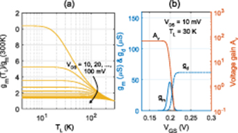
Figure 2. (a) The boost of gm at low temperature compared to room-temperature, at different VDS , reaching up to a factor 10 at low temperature and bias conditions. This gm enhancement effect is unique to quantized transistors, as traditional FETs typically only show weak temperature dependence for gm . (b) Transconductance and output conductance at VDS = 10 mV and TL = 30 K. Voltage gain Av at the first energy band is 10.
Download figure:
Standard image High-resolution image
Figure 3. (a) Hybrid-π small signal model for a 1D-LNA based on parasitics from a structure similar to the simulated one [20]. (b) Current gain |h21|2, maximum stable gain |MSG|, maximum available gain |MAG| and stability factor K as a function of frequency. (c) The value gm /√IDS as a function of IDS for the 1D-LNA and the cryogenic HEMT. Transconductance as a function of the drain current is also presented. (d) Linearity performance of a 1D-LNA depending on input amplitude (5 and 30 mV). Output of 30 mV input signal is heavily distorted.
Download figure:
Standard image High-resolution imageA large value of gm /√IDS is desirable in order to minimize Tmin. In figure 3(c) we show that the maximum value gm /√IDS (16.8 mS/√mA/√µm) for the 1D-LNA is 3x larger than a state-of-the-art cryogenic HEMT [6]. gm versus IDS is also shown to confirm that the bias point of minimum noise approximately correlates with that of maximum gain. Tmin can also be expected to be strongly reduced compared to a standard HEMT due to the lower power dissipated in the device, which will reduce the drain equivalent noise temperature. However, accurate estimate of Tmin will require experimental characterization. In addition, gate leakage can contribute significantly to Tmin in fabricated devices. Due to the presence of a gate oxide in the proposed device, the gate leakage is expected to be lower than in a HEMT.
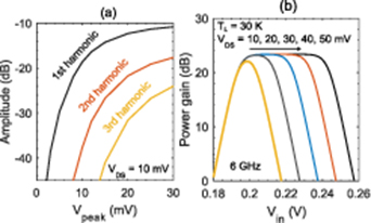
In the 1D-LNA, there is a trade-off between linearity and DC power. The gm peak width is proportional to both TL, VDD and maximum gm , and will determine the linearity of the amplifier at a given AC input voltage amplitude, Vpeak. Next, we study the linearity characteristics of the proposed device. Figure 3(d) shows time-domain simulations of the input bias and output current for a high-bias (Vpeak = 30 mV) and a low-bias (Vpeak = 5 mV) small-signal input amplitude. The low-voltage signal accurately outputs the sinusoidal input signal (quasi-linear condition), while the high-bias signal is distorted due to the non-linear features of the transfer characteristics. Figure 4(a) shows the amplitude of the harmonic signals as a function of Vpeak, relative the fundamental frequency of amplitude 0 dB, at VDS = 10 mV. The harmonics are obtained from Fourier analysis of the output signal. The amplitudes of the higher harmonics are a measure of the distortion introduced by the gm characteristics. We observe that at this drive bias, the input bias AC amplitude Vpeak should be less than 5 mV to obtain highly linear conditions. This means that the typical 10–100 μV transmon qubit readout signals are well suited for this type of amplifier [22, 23]. Figure 4(b) shows the maximum available power gain as a function of the DC bias point of the input signal Vin, and the drive bias VDS at 6 GHz (a typical transmon operation frequency). The plateau of the gain indicates the linear region of the amplifier. Since gm = T2q2/h is independent of VDS , only the width of the gm peak increases, not the peak value, which gives rise to this linear region. The physical explanation for this behavior is that an applied VDS opens a conducting window eVDS , between the source and drain side Fermi levels, and as the bottom of a subband is swept through the window by Vin, gm re'dened to correspond to the applied VDS .
Figure 4. (a) Amplitudes of the 1st, 2nd and 3rd harmonics generated at the output from the sinusoidal input signal shown in figure 2(d) at VDS = 10 mV. The fundamental frequency is normalized to 0 dB. These amplitudes quantify the distortion introduced by the amplifier and show that input bias amplitudes of below 5 mV can be handled quite well at this drive bias. (b) Power gain versus DC input level and drive bias. The plateau of the gain curve indicates the linear region of operation and is due to the physics of the quantized channel, as the transconductance is decoupled from VDS.
Download figure:
Standard image High-resolution image
In Table 1 we compare the cryogenic HEMT [6] to the 1D-LNA for two different drive voltages 10 and 50 mV at temperatures 30 and 100 K respectively. In terms of power dissipation, the 1D-LNA at 10 mV outperforms the HEMT by a factor of 40. We also state a higher level of current gain at 10 GHz, which leads to a 49x better gain to power ratio for the 1D-LNA. The improved performance is mainly due to the gm boost at low temperatures, but as shown, comes at the price of linearity and is only valid for low-power input signals.
Table 1. Comparing HEMT with 1D-LNA (this work).
| Metric | Unit | HEMT @ 5 K [6] | 1D-LNA @ 30 K this work | 1D-LNA @ 100 K this work |
|---|---|---|---|---|
| PDC @ IDS = 5 mA | (mW) | 2 | 0.05 | 0.25 |
| VDS | (mV) | 400 | 10 | 50 |
| fT | (GHz) | 188 | 380 | 450 |
| |h21|2 at 10 GHz | (dB) | 26 | 32 | 33 |
| Gain for power | (B/mW) | 13 | 640 | 132 |
 (max) (max) |

| 5.1 | 16.8 | 9.6 |
We note, finally, that while the transconductance boosting effect has been observed in a suitable device architecture, the remaining experimental challenge is to achieve this effect in a MOSFET with a sufficient number of relatively homogenous parallel nanowires in order to obtain large enough drive current to run the LNA circuit. While we used 300 parallel nanowires for our simulations, this is simply to allow accurate comparison to standard devices. The actual number of needed nanowires will depend on the application and LNA design and could be significantly lower.
4. Conclusions
We proposed and simulated the concept of a 1D-LNA that uses a quasi-ballistic MOSFET with a scaled nanowire channel showing quantization of energy levels. At cryogenic temperatures, this device achieves up to 10 times boost of the peak transconductance compared to room-temperature. This means that the device can be operated at up to 40 times lower PDC compared to standard HEMTs, while achieving similar gain and likely reduced noise temperature. PDC down to 50 μW is possible, indicating the feasibility of operation at sub-Kelvin cryostat temperature stages. While the device shows lower linearity compared to a standard amplifier, it is sufficient for low-power input signals. This type of device shows great promise for the qubit readout in quantum computer applications, where the reduced noise and power can enhance the scalability of the quantum system.
Acknowledgments
This work was supported by European Union H2020 program SEQUENCE (Grant—871764).