
Abstract
p-Si/4H-SiC heterojunction diodes are realized by sputter-deposition of the Si top contact and subsequent post-deposition annealing at either 900 °C or 1000 °C. The high Schottky barrier height (SBH) of this junction architecture of around 1.65 V is ideal to analyze SBH inhomogeneities present in most Schottky- and heterojunctions. Current-voltage-temperature (IVT) and capacitance-voltage-temperature (CVT) measurements are conducted in a wide temperature range from 60 K up to 460 K while applying standard techniques for SBH extraction. Strong deviations from ideal IV characteristics are present especially at lowest temperatures when assuming a homogenous SBH. Additionally, the extracted SBHs at low temperatures differ a lot between the two methods, indicating the presence of low barrier conduction paths. The presence of at least two distinct SBH inhomogeneities is found, which are labeled as 'intrinsic' and 'extrinsic'. Next, the Tung model was applied to fit the measured IVT data using a discretized Gaussian distribution of patch parameters to account for spreading resistance effects. By using multiple Gaussian distributions, excellent fitting results were achieved, giving the density values of the different patches and a background barrier height from the IVT data, which are in excellent agreement with the CVT data over a wide temperature range of 400 K.
Export citation and abstract BibTeX RIS

Original content from this work may be used under the terms of the Creative Commons Attribution 4.0 license. Any further distribution of this work must maintain attribution to the author(s) and the title of the work, journal citation and DOI.
1. Introduction
Silicon carbide (SiC) is of high interest as a semiconductor material for power electronics for many years now. With the availability of cheaper and large diameter substrates, more and more advanced device architectures emerged [1]. Schottky diodes were one of the first commercially available SiC devices. Breakdown voltages of several kilovolts are reported along with very fast switching times of less than 30 ns [2–7]. In the last decades, Schottky-contacts (SCs) on several SiC polytypes with a variety of metals have been characterized [8–10]. In recent years, the focus was on the 4H-SiC polytype due to its wider bandgap of 3.26 eV, higher mobilities, and shallower doping levels [11, 12].
When it comes to the characterization of SCs, electrical measurement techniques, especially current-voltage (IV) and capacitance-voltage (CV) are the most relevant. Extractions of the Schottky barrier height (SBH) φB by fitting the thermionic emission (TE) equation to the experimental data is fast and straight-forward. Independent of the semiconductor, IV-curves showing double or multiple bumps in the semi-logarithmic IV data [13–17], unusually high, and bias dependent ideality factors [18, 19], as well as non-linear Richardson plots [20, 21], have been observed. In addition, deviations from the SBH derived from IV and CV measurements are frequently observed. The most likely reason for these deviations from the ideal behavior can be attributed to a spatially inhomogeneous barrier height across the metal-semiconductor (MS) interface. To determine this impact, first experiments date back in the 1980s [21–23]. A nonuniformity of the SBH across the interface is obvious, as most MS interfaces are made of a polycrystalline metallization, consisting of regions with different crystallographic orientations as well as grain boundaries. These effects lead to varying local interface properties, and in further consequence, to a nonuniform charge distribution and barrier heights, respectively. Also, unintentional contaminations by e.g. residues on the surface, and crystal defects at the substrate surface can account for a local variation of the SBH. Even the random distribution of dopant atoms and dangling bonds close to the surface can be responsible for slight variations of the local SBH [24]. One very intuitive way to model the current transport over an MS junction with different SBHs would be to split the junction into parallel paths, each having a constant SBH and covering a fraction of the total area. Then the total current over the junction is a summation of the TE current of each individual patch. This approach is called the parallel conduction model [25] and works well for individual patch sizes larger than the semiconductor Debye length [26]. If the patch dimensions are rather small compared to the Debye length, an effect called 'pinch-off' significantly increases the SBH of a low barrier patch surrounded by a high barrier region [27, 28]. Werner and Gütter [20] derived a theory based on the parallel conduction model, assuming a Gaussian distribution of the SBHs, but neglecting any pinch-off effects. Although they were able to model many effects like the temperature dependence of the ideality factor and the deviating results between SBHs evaluated by CV and IV measurements, the influence of the semiconductor doping concentration on the observed inhomogeneity effects was not described well. Tung [28, 29] was the first to propose a model to describe barrier height inhomogeneities considering the pinch-off effect and was able to describe most of the measured deviations from ideal IV curves and ideality factor effects like the T0-anomaly [30, 31]. His theory considers the impact of the surrounding high barrier region on the potential distribution around a patch with lower SBH. Especially when considering small patch sizes, low doping concentrations and high forward bias levels, the local potential distribution underneath a low SBH patch does not decrease linearly, but pinches off close to the surface, resulting in a potential barrier higher than the surface potential. The new potential barrier is designated as 'saddle-point potential'. This so-called potential pinch-off is responsible for the measured doping and voltage dependencies of the SBH inhomogeneities. By introducing a single dipole approximation, Tung was able to derive an analytical solution to calculate the saddle-point potential as a function of voltage, doping concentration, temperature, the patch radius and SBH of the low SBH patch. This analytical solution is in good agreement to numerical simulations [27]. Ballistic electron emission microscopy (BEEM) measurements of artificially generated inhomogeneous SCs were able to proof the model of pinch-off as proposed by Tung [32, 33]. By fitting the Tung model in combination with a Gaussian distribution of the patch parameter reasonable results were achieved on different SCs, further validating its ability to describe the current transport of most real SCs [18, 34, 35].
About 20 years ago the combination of Si and 4H-SiC was first reported in literature, demonstrating its potential by offering good rectifying properties depending on the doping type of each individual semiconductor material [36]. Heterojunction diodes (HJDs) have been prepared and characterized for Si on SiC directly grown by chemical or physical deposition techniques [2, 36, 37] or using surface activated bonding [38–41]. Due to its availability, research mainly focused on n-type SiC as substrate, so that heterojunctions using n-Si, forming an isotype n-N heterojunction, and p-Si, forming an anisotype p-N heterojunction, have been characterized. Due to the huge band offset of about ΔEC ∼ 0.5 eV and ΔEV ∼ 1.5 eV, the heterojunction can be treated in good approximation as a unipolar device. In case of n-type SiC, electrons are the main charge carriers. Due to this unipolar nature, the current transport over the junction can be treated similarly to an SC using TE theory, with the SBH and the ideality factor as characteristic quantities. Theory and measurements predict rather low SBHs for n-N HJDs in the range 0.6 to 1 V, whereas the SBH tends to decrease with increasing n-Si doping concentration. The p-N heterojunction shows rather high SBHs of about 1.5–2 V, increasing when enhancing the doping concentration of the p-Si contact material [36, 42].
In this study, HJDs were realized by depositing polycrystalline p-Si on monocrystalline n-type 4H-SiC. These devices were characterized electrically over a large temperature range from 60 K to 460 K to evaluate SBH inhomogeneities. Due to the high boron doping, the p-Si contact can be treated like a metal, resulting in a negligible voltage drop in the contact material. Therefore, no depletion region forms in the poly-Si, and all the band bending is limited to the low-doped 4H-SiC epitaxial layer. The relatively high SBH of this junction is well suited to investigate SBH inhomogeneities, as low barrier regions of small size will stand out from the high SBH background. In addition to the detailed characterization of the p-Si/4H-SiC heterojunction over a wide temperature range never reported before, we applied the Tung model to the experimental data to get a deeper insight into the local distribution of barrier height inhomogeneities.
2. Experimental details
For diode fabrication, 4H-SiC substrates supplied by Cree Inc. with a nitrogen bulk doping concentration of ND = 1019 cm−3 and a 5 µm thick epitaxial layer with ND = 1.6 × 1016 cm−3 are used. Prior to p-Si deposition, the substrate was cleaned in acetone followed by a standard Radio Corporation of America (RCA) clean. An approximately 1 µm thick layer of amorphous Si (a-Si) was sputter deposited from a highly boron-doped Si target (ρ < 0.005 Ω cm) with 6 N purity. A Von Ardenne LS730S DC magnetron sputtering system with a sputtering power Pdc = 500 W and a chamber pressure p= 0.3 Pa was used for deposition. With these parameters, the deposition rate was measured to be about 1.2 nm s−1. The sample was not actively heated during film synthetization, so that only plasma-induced self-heating took place. The as-deposited samples underwent a post-deposition annealing (PDA) step to crystallize the a-Si to poly-Si. The PDA process was carried out in a quartz tube furnace in high vacuum (<1 mPa) for 2 h at 900 °C and 1000 °C, respectively. The heating ramp was 5 °C min−1, whereas the cool down phase was not controlled. After the PDA, the samples were dipped in hydrofluoric acid (HF) before sputter depositing a bilayer of 200 nm Ti and 200 nm Pt on the backside. To form ohmic contacts a subsequent annealing step at 1000 °C for 1 min. in a rapid thermal annealing oven was performed for alloy formation. After this annealing step another 100 nm Pt was sputter deposited on the backside serving as surface protection and to provide good electrical contact. Next, the sample was again etched in HF to remove any oxide from the poly-Si, before 200 nm Mo was sputter deposited on the front side. Two lithography processes were applied to pattern the Mo and the underlying poly-Si into circular pad structures by individual wet etching steps. The Mo contacts are slightly smaller in diameter to prevent any electrical short-cut to the substrate. The two-step etching process of Mo and poly-Si was done in aqua regia and in an isotropic silicon etch mixture (10% HF(48%) + 70% HNO3(65%) + 20% H2O), while the back contact was protected by photoresist. The final, circular-shaped area of the active heterojunction is 0.5 mm2. Ohmic contact formation of the Mo to the poly-Si was verified by circular transmission line test structures. Using secondary ion mass spectroscopy, the boron concentration of the deposited and annealed Si films was measured to be (9 ± 2) × 1019 cm−3. The electrically active concentration must be assumed lower due to the polycrystalline nature of the Si layer. Microstructural analysis of as-deposited and post annealed poly-Si films has been reported previously [43].
Electrical measurements were conducted in a dark, electrically shielded cryo/heating chamber under vacuum in a temperatures range of 60 K to 460 K in 20 K steps. IV measurements were done with a Keysight B2985A electrometer from 0 V to −20 V in 500 mV steps and from 0 V to 2 V in 15 mV steps while setting the current compliance to 20 mA. CV measurements were done using an Agilent 4294 A high precision impedance analyzer at 1 MHz test frequency in a voltage range of −2 V to 0.5 V. The voltage sweep direction was from negative to positive values and back.
3. IVT and CVT measurements
In this section, the classic evaluation methods for both IVT measurements using the TE equation and for CVT measurements are applied to determine the SBH. SBHs determined from IV measurements are designated φB and those from CV as φB, CV.
The IV relationship of a homogenous SC can be derived from TE theory as
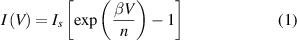
where n is an empirical ideality factor and β = q/(kT) with the elementary charge q and the Boltzmann constant k. The ideality factor should be 1 for solely thermionic emission across a homogeneous barrier. Deviations from unity are attributed to the contribution of tunneling current and the presence of SBH inhomogeneities. The saturation current is given by

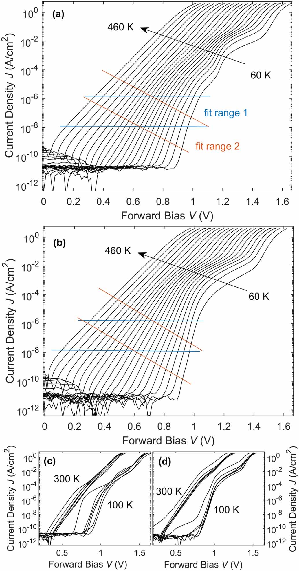
with A* being the Richardson constant (for 4H-SiC: A* =146A K−2 cm−2 [44]), A the contact area, T the absolute temperature and φB is the SBH. When plotting the forward-biased IV data in a semi-logarithmic plot as log(I) over V, the saturation current Is and the ideality factor n are determined by a linear fitting procedure from the y-axis intercept and the inverse slope, respectively. The SBH φB follows from Is . Figures 1(a) and (b) show the measured IVT data of two selected, representative diodes with post-deposition annealing at 900 °C and 1000 °C, respectively. No major deviation was found between different diodes, which justifies the selection of these two for the fitting experiments. Especially at low temperatures, strong deviations from the ideal, linear characteristics are observed. Two, or in some cases even three bumps in the IV data are present. These bumps are representative for regions with lower SBH than on average being present across the diode area. At low temperatures, the current is predominantly flowing through regions with the lowest SBH until they become saturated. At temperatures T > 300 K, the curves start to become more ideal and at T > 400 K, the IV curves are almost linear. This behavior is as expected because at elevated temperatures enough charge carriers can pass directly over the higher background barrier, whereas the current fraction over the relatively small regions with a low SBH is limited and hence, has a negligible impact on the overall device performance. In figures 1(c) and (d), IV measurement cycles of six diodes originating from the same two wafers are depicted at two temperatures. All measured diodes show similar characteristics with multiple bumps at T = 100 K, predominantly in a region where the current flow is dominated by low SBH patches. At 300 K, the deviations become even smaller.

Figure 1. IVT measurements of heterojunction diodes annealed at (a) TPDA = 900 °C and (b) TPDA = 1000 °C. Lines indicate two current ranges used for fitting. (c) and (d) show at two temperatures the superposition of six diodes of the same wafer annealed at 900 °C and 1000 °C, respectively.
Download figure:
Standard image High-resolution imageIn the depicted IVT data, two current regions are indicated, which are used for fitting. Fit range 1 is constant, whereas fit range 2 is temperature dependent, thus accounting for the huge measurement temperature range. The extracted parameters of two diodes are shown in figure 2. In the upper two graphs, φB and n are plotted as a function of temperature. The extracted parameters from these two different fit ranges match very well at elevated temperatures. At lower temperatures, however, the deviations become more dominant. This is obvious as the IV curves are no longer linear, but slightly curved, resulting in bias dependent φB and n values, which is common for inhomogeneous SCs [18, 19, 28]. Due to the non-linearity of the IV curves at low temperatures, the extracted values are strongly dependent on the used fitting range and need to be considered carefully. Furthermore, strong temperature dependence of both parameters is observed. The SBH is very low in the range of 0.4 to 0.6 V at 60 K but increases substantially with temperature until it tends to saturate. For the 900 °C annealed sample this device parameter almost reaches a value of 1.56 V at T = 460 K, while it is 1.52 V for the 1000 °C annealed sample. This difference of about 40 mV in the maximal SBH at these two annealing temperatures is seen across many samples. We attribute these deviations to different crystallographic properties, e.g. grain size, in the poly-Si film due to the different annealing temperatures [43].

Figure 2. (a), (b): Extracted SBH φB and ideality factor n of the two diodes displayed in figure 1. (c), (d) Plot of nkT over kT showing the temperature dependence of the ideality factor. The straight line indicates the ideal case of n = 1. The colors correspond to the two fit regions shown in figure 1. Error bars indicate the 95% confidence interval of the parameter due to fitting.
Download figure:
Standard image High-resolution imageAt the lowest measurement temperatures, the ideality factor is very high, ranging between 2 and 3, and decreases towards 1 as the temperature is increased. At room temperature n is already below 1.1 and reaches values as low as 1.03 at T = 460 K. The lower two plots depict the temperature dependence of n in a different form along with the ideal case of n = 1. This way of plotting is ideal for identifying the temperature dependence of n [31]. The measured ideality factors are almost parallel to the unity slope, therefore representing the T0-anomaly. Only at the lowest temperatures, a slight deviation from the straight line is visible, reflecting a starting contribution of tunneling currents. The T0-anomaly is typical for inhomogeneous MS contacts and the theory by Tung explains it very well [28].
To further investigate the fabricated HJDs, CVT measurements have been conducted between 60 K and 460 K at a test frequency of 1 MHz comprising of an up- and downward voltage sweep to detect any hysteresis. The SBH is calculated using the built-in potential ψbi and the Fermi potential φn by

with Δφ being the image force lowering. (−ψbi + kT/q) is obtained as the x-axis intercept of a C−2 over V plot [45]. The Fermi potential is calculated analytically for all temperatures, considering all important temperature dependencies of 4H-SiC. The effective densities of states (DOS) require the temperature dependence of the effective DOS masses mdc * and mdv * for 4H-SiC. Wellenhofer and Rössler [46] calculated mdc * and mdv * and Hatakeyama et al [47] derived a polynomial fit which was used for calculation. The Fermi potential than follows from calculating the Fermi level using the most general Fermi–Dirac distribution [48] along with considering incomplete ionization. For nitrogen in 4H-SiC one often uses an effective ionization energy ED,eff of 70 meV, which is about the average of the two ionization energies [49]. The effect of image force lowering is neglected in this study. At 300 K and zero bias, Δφ would calculate to be about 36 mV. The doping concentration is given by
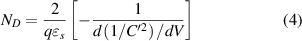
with  s
being the permittivity of the semiconductor and C' the capacitance per cm2. The extracted parameters are depicted in figure 3. All graphs have in common, that the measuring points at the lowest two temperatures deviate strongly from the overall trend. These data points do not reflect the true value but are artifacts from the beginning resonance of the dopant states. At these low temperatures, the time constant of the cubic site nitrogen donor start to match with the measuring frequency, resulting in measured capacitances different from those given by the depletion width [50]. When neglecting these data points, the SBH values using the CV method φB,
CV are about 1.7 V at low temperatures, whereas this parameter slightly decreases to 1.6 V at T= 460 K. The second sample, which was annealed at 1000 °C, shows the same trend in SBH. The shape of the measured temperature dependence of the SBH agrees with the predicted trend of decreasing SBH with temperature considering temperature dependencies of the bandgaps of the two materials. It strongly deviates from the IVT obtained values, because the CV method gives the mean SBH φB
0
across the whole diode area [51, 52]. Despite these differences, the extracted SBH values of both methods are in good agreement at high temperatures. The measured doping concentration is within the specifications of the 4H-SiC epitaxial layer as given by the manufacturer. No notable difference between the two sweep directions is observed, indicating no hysteresis effects.
s
being the permittivity of the semiconductor and C' the capacitance per cm2. The extracted parameters are depicted in figure 3. All graphs have in common, that the measuring points at the lowest two temperatures deviate strongly from the overall trend. These data points do not reflect the true value but are artifacts from the beginning resonance of the dopant states. At these low temperatures, the time constant of the cubic site nitrogen donor start to match with the measuring frequency, resulting in measured capacitances different from those given by the depletion width [50]. When neglecting these data points, the SBH values using the CV method φB,
CV are about 1.7 V at low temperatures, whereas this parameter slightly decreases to 1.6 V at T= 460 K. The second sample, which was annealed at 1000 °C, shows the same trend in SBH. The shape of the measured temperature dependence of the SBH agrees with the predicted trend of decreasing SBH with temperature considering temperature dependencies of the bandgaps of the two materials. It strongly deviates from the IVT obtained values, because the CV method gives the mean SBH φB
0
across the whole diode area [51, 52]. Despite these differences, the extracted SBH values of both methods are in good agreement at high temperatures. The measured doping concentration is within the specifications of the 4H-SiC epitaxial layer as given by the manufacturer. No notable difference between the two sweep directions is observed, indicating no hysteresis effects.

Figure 3. SBH φB, CV and doping concentration ND evaluated using CV measurements in a temperature range of 60 K to 460 K at 1 MHz test frequency. The sweep direction was altered between upwards (up) and downwards (down). Left figures annealed at TDPA = 900 °C, right figures at TDPA = 1000 °C. Insets (b) and (d) show the raw CV data at 60 K, 100 K, 200 K, 300 K and 400 K from bottom to top. Error bars indicate the 95% confidence interval of the parameter due to fitting.
Download figure:
Standard image High-resolution image4. Parameter extraction using the Tung model
Due to the strong non-idealities observed in the IVT measurements and due to the strong deviations of the SBH determined using IV and CV methods especially at lower temperatures, the presence of local inhomogeneities at the interface is evident. Therefore, we will apply Tung's model [28] to reconstruct the measured IVT data using an approach similar to Gammon [18], who discretized the Gaussian distribution to account for the resistive impact of patches.
To further emphasize the need of considering inhomogeneous SBH distributions, figure 4 depicts one of the measured IV curves at the lowest temperature, together with a calculated ideal IV curve with one homogenous barrier of φB 0 = 1.7 V, which is about the value determined using the CV technique and is assumed to be close to the true background barrier height. As can be seen, even at high bias values, the measured IV curve is shifted towards lower voltages compared to the ideal curve with a homogenous SBH. Due to the bump at lower voltages, the deviation from the homogenous case is even worse. This discrepancy can best be described using the schematic illustration of the assumed SBH distribution in figure 4(b).

Figure 4. (a) Measured IV characteristic at T = 60 K of the 1000 °C annealed heterojunction diode along with the theoretical IV curve of a diode with a uniform barrier of φB 0 at T = 60 K. Two regions of the measured curve are assigned which are assumed to be dominated by individual Gaussian distributions of barrier inhomogeneities representing both intrinsic and extrinsic sources, respectively. (b) Schematic illustration of the barrier height distribution at a certain voltage marked by a red circle mark in (a). Blue filled areas indicate barriers that contribute to the current transport.
Download figure:
Standard image High-resolution imageWe suppose the SBH distribution can be described by two distributions of barrier heights plus the background barrier φB 0 . The lower distribution consists of low SBH patches of larger size being of mostly 'extrinsic' origin, e.g. contaminations. Depending on the source of contamination, several distributions may be needed for accurate modeling. Low densities of rather large low SBH extrinsic defects have been suggested earlier to describe the distorted low voltage IV characteristic of Schottky diodes [14, 16]. The second distribution is centered around the average background barrier φB 0 and is assumed to be based on an 'intrinsic' source like defects in the semiconductor, local dopant fluctuations and variations in the surface potential due to e.g. grain boundaries. Typically, intrinsic inhomogeneities are associated with small-sized patches. Similar assumptions of multiple patch distributions have been made before [53–56]. Vanalme et al [57] performed BEEM measurements on different III–V semiconductors and found experimental evidence of SBH distributions of at least two Gaussian distributions. The dependence of the secondary distributions on surfaces undergoing different pre-treatments might be seen as an evidence of their extrinsic origin. Gaussian distributions with two different mean values have also been measured using BEEM on electrochemically prepared Au/GaAs diodes [52].
The distribution in figure 4(b) is only valid at a certain voltage and is not to scale. As will be seen in the fitting results, the extrinsic inhomogeneities cover a much lower fraction of the total area than the intrinsic distribution and the background. The background covers >90% of the interface area. The blue filled area in the distribution represents the barriers that are contributing to the current flow. The corresponding point in the IV domain is marked by a red circle in figure 4(a). This region of contribution is strongly temperature and voltage-dependent, thus substantially influencing the shape of the measured IV characteristics, especially at low temperatures. At lower forward voltages, only the extrinsic inhomogeneities contribute to the current flow until they are saturated and the parasitic ohmic resistance starts to dominate. If the voltage is further increased, the intrinsic barrier distribution starts to contribute as well, allowing for a strong increase of the current. At low temperatures, the ohmic fraction starts to limit the current flow before the background barriers can even contribute to the current. At higher temperatures, the charge carrier distribution is no longer as sharp, but much more blurred as a result of the Fermi–Dirac distribution. Therefore, the background barrier contributes to the current flow as well.
In the most general case, the total current over an inhomogeneous SC can be described as a combination of patches that are pinched-off ('p-o'), patches that are not pinched-off ('not p-o') and the current over the homogenous background like
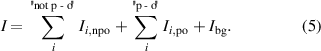
The individual current fractions follow by
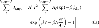
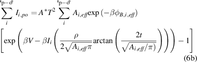

All three components are based on the TE equation (1). In the case of not pinched-off patches, the interface is divided like in the parallel conduction method with each patch having its individual area Ai and SBH φB,i . The pinched-off patches are described in the same way, but with each patch having an effective area Ai, eff and an effective SBH φB,i, eff. In contrast to the not pinched-off patches, these effective parameters are dependent on the doping concentration, the applied voltage, and the temperature. Due to the partially very small cross-sectional areas of the pinched-off patches, the series resistance of a patch can be very spreading in nature and is therefore considered in the most general case for circular shaped pads [24, 58]. The last contribution considered is that from the background, which is the region embedding the patches, and which is assumed uniform in barrier height. Other quantities used in the equation are the SiC epi-layer thickness t and resistivity ρ and the overall device series resistance R, which mainly consists of the ohmic contacts to the p-Si and to the SiC substrate on the backside.
Tung [27, 28] found a good approximation to describe the pinch-off effects using a point-dipole approximation. He showed that circular patches with a radius R0 and a barrier height φB 0-Δ can be described using a single patch parameter
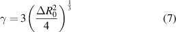
where Δ is the difference to the mean background barrier height, which can be of either sign. Using this patch parameter, the effective SBH, the effective area, and the effective ideality factor of a patch with a patch parameter γi can be calculated by
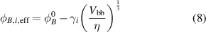
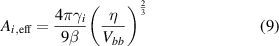
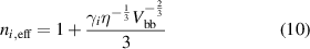
with Vbb = φB
0—φn—V being the band bending, and η = s
/(qND
). Band bending and built-in potential are related via ψbi = Vbb(V= 0). Here, and for the calculation of the depletion width W, the carrier concentration ND
is assumed to be the total number of donors, hence complete ionization is assumed. This assumption is valid and mandatory if the device is operated in static mode (no switching faster than the ionization time constants). In static operation, full ionization in the depletion layer occurs due to Poole-Frenkel ionization [59]. During the slow voltage sweep in IVT characterization, this condition is met at T > 40 K [60].
Although Tung also provided an equation considering a Gaussian distribution of the patch parameter, it does not consider the resistive effects of individual patches. Therefore, the Gaussian distribution of patch parameters is discretized using a mean patch parameter γ0 and its standard deviation σγ
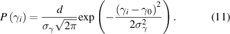
The discretization width d of γi
must be chosen in a way to normalize  . With a discretization of the patch parameter γi
, the number of patches with a certain γi
is CpP(γi). Cp
is the total number of patches and CpP(γi) is the number of patches with the same patch parameter, depending on the discretization. Using this discretization, the current over an inhomogeneous interface does not have to be summed up for each individual patch, but patches with the same parameter γi
can be treated jointly and the series resistance can still be considered. Therefore, equations (6
a) and (6
b) translate to (12
a) and (12
b) in which the index i is now the number of discretization steps.
. With a discretization of the patch parameter γi
, the number of patches with a certain γi
is CpP(γi). Cp
is the total number of patches and CpP(γi) is the number of patches with the same patch parameter, depending on the discretization. Using this discretization, the current over an inhomogeneous interface does not have to be summed up for each individual patch, but patches with the same parameter γi
can be treated jointly and the series resistance can still be considered. Therefore, equations (6
a) and (6
b) translate to (12
a) and (12
b) in which the index i is now the number of discretization steps.
4.1. Fit using 2 Gaussian distributions
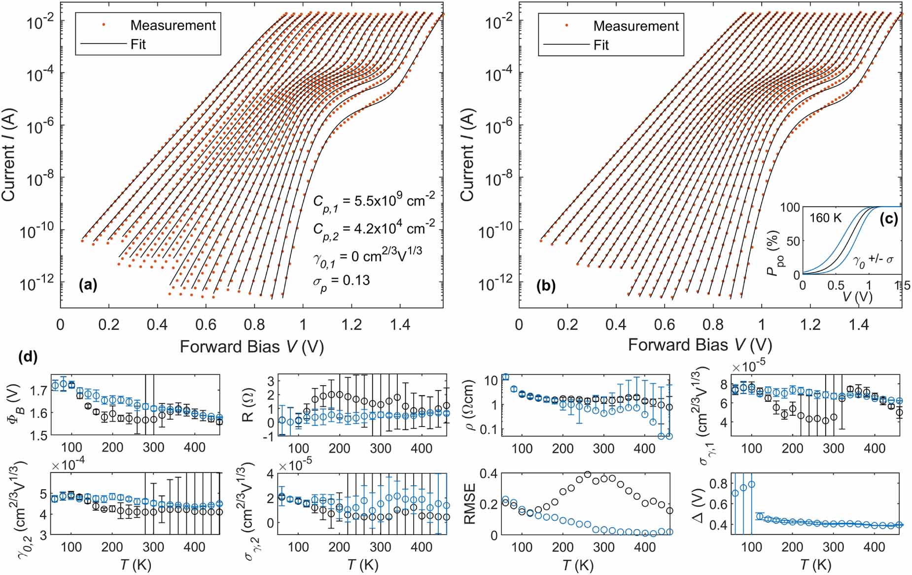
In a first approach, we try to fit the IVT data of the 1000 °C annealed heterojunction diode depicted in figure 1(b) using the Tung model, with the approximation of all patches being effected by pinch-off. The IVT data of this diode clearly shows a double bump, indicating the need of at least two barrier height distributions. Therefore, two Gaussian distributions of the patch parameter γi are used for the fitting procedure, representing the extrinsic and the intrinsic patches, which are centered around φB 0 . All relevant parameters used for fitting are listed in table 1. The indices of the fit parameters indicate the distribution to which they belong. For example, Cp,1 is the density of the first distribution counted from high barriers downwards. Some of the parameters displayed in table 1 are not used in the first fit. For the patch densities and the mean patch parameter of the intrinsic distribution, no temperature dependency is expected, and hence, they were kept constant. Least-squares fits of equations (5), (6 c) and (12 b) were conducted. The optimal values for the temperature-independent quantities were determined by performing the fit several times, varying these constants until the error was minimized. The resulting fit curves are depicted in figure 5(a), while labeling the optimized temperature-independent quantities in the figure. Those, which are temperature dependent, are depicted in figure 5(d).
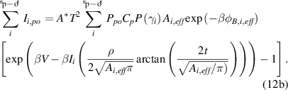

Figure 5. (a) Measured data and least-squares fit of the 1000 °C annealed sample. (b) Same data as in (a) but fit considering the not pinched-off patches. (c) Weight function for pinch-off to not pinch-off ratio. (d) Fitting parameters as a function of temperature. Black belong to (a); blue belong to (b). The temperature-independent fit parameters are the same and are labeled in (a). Error bars indicate the 95% confidence interval of each fitting parameter.
Download figure:
Standard image High-resolution imageTable 1. List of parameters used for fitting the measured IVT data. *a Additional parameters applied during the fitting procedure considering pinched-off and not pinched-off patches. *b Additional parameters applied during the fitting procedure when assuming three patch parameter distributions.
| Fit Parameter | Description | Expected temperature dependency |
|---|---|---|
| Cp,1 | Density of patches of the intrinsic distribution | No |
| γ0,1 | Mean value of the extrinsic distribution. Centered around φB 0 | No |
| σγ,1 | Standard deviation of the intrinsic distribution | Weak |
| Cp,2 | Density of patches of the extrinsic distribution | No |
| γ0,2 | Mean value of the extrinsic distribution | Weak |
| σγ,2 | Standard deviation of the extrinsic distribution | Weak |
| Cp,3 *b | Density of patches of the extrinsic distribution | No |
| γ0,3 *b | Mean value of the extrinsic distribution | Weak |
| σγ,3 *b | Standard deviation of the extrinsic distribution | Weak |
| φB 0 | Mean background SBH | Yes |
| ρ | 4H-SiC epi-layer resistivity | Yes |
| R | Series resistance | Weak |
| σp *a | Shape parameter of the weight function | No |
| Δ *a | SBH difference of a patch from the background | Yes |
The quality of the fitting procedure is estimated by the root-mean-square error (RMSE), which is also plotted as a function of temperature. At the lowest temperatures investigated, the fit is very accurate, only the region of the resistive current limit of the extrinsic inhomogeneities is not reflected very well. The measured IV data increase with voltage stronger than an ohmic limit would allow. This might be addressed either by small amounts of patches in between the two assumed Gaussian distributions or by the effect of Pool-Frenkel ionization happening underneath the small patches. Very high current densities, hence field strength could result in partially enhanced dopant ionization underneath the conducting patches even at these low temperatures. Nevertheless, due to the already very complex model, these effects are not considered. Starting at about 160 K, the fit starts to get worse, especially at low bias values, regardless of the starting parameters or the values of the temperature-independent parameters. An in-depth analysis showed that the steepness, hence ideality factors, of the IV curves in these regions is larger than Tung's model would predict. Even a single low SBH patch would not be able to reproduce the measured IV characteristics in this bias and temperature range, thus demonstrating the main limitation of the Tung model. To calculate the pinch-off effects and therefore the effective SBH and effective areas, Tung approximates a circular area of lower SBH using a single point-dipole and shows, that this approximation is well justified if the patch radius is much smaller than the semiconductor depletion width (R0 ≪ W). The intrinsic inhomogeneities are usually very small in size and consequently, meet this pre-request. The extrinsic inhomogeneities, however, originating mostly from external contaminations are typically 10 to 100 nm in radius and cannot be approximated by a single point-dipole. An exact solution of the potential distribution underneath such semi-large patches is only possible by a numerical solution of the Poisson equation or in very good approximation by a dipole layer instead of a point-dipole, requesting high computing power. If the patches are large enough they can be considered as not pinched-off and are describable using the parallel-conduction model and equation (12 a). Sullivan and Tung came up with a condition whether pinch-off effects are occurring, depending on the patch radius, the patch SBH depth, the semiconductor doping, and the applied voltage
In the case of the diodes investigated in this study, the extrinsic SBH patches are likely in a range where they fulfill this condition depending on the applied bias, but still the condition R0 ≪ W is not fulfilled in most cases. Due to the combination of the used doping concentration and the size of the extrinsic low SBH patches, a treatment as only pinched-off is just as impossible as a treatment as only not pinched-off. In order to continue working with the classic Tung model, the following workaround was chosen. In the equations (12 a) and (12 b) the parameter Ppo is introduced as a weight function of the pinch-off to not pinch-off ratio. Ppo(Rcrit /R0 ) = 1 is equivalent to 100% of the patches being affected by pinched-off at a certain voltage and patch parameter. For the weight function Ppo several functions have been tested. By requesting some basic conditions like being a differentiable function, Ppo(Rcrit /R0 ≪ 1) = 0 and Ppo(Rcrit /R0 ≫1) = 1 and Ppo(Rcrit /R0 = 1) = 0.5 we decided to use the cumulative distribution function of the log-normal distribution as following
where Rcrit = ΔW/2Vbb follows from equation (13) and indicates the critical ratio where pinch-off is assumed to occur and σp is a shape parameter used in the log-normal distribution. Because we work with the patch parameter γ, R0 and Δ are not distinguished until now. However, for considering the not pinched-off patches this has to be done. Therefore Δ is now used as an additional fit parameter. Using equation (7) R0 can be calculated for every γi . Another approximation that was done here is to assume Δ not to be of Gaussian distribution, but only the patch radius R0 . Assuming the extrinsic patches to be mainly of the same source of contamination, they may be of similar SBH but vary slightly in size. Now for every γi and every voltage V, Ppo can be calculated and the current contributions from equations (12 a) and (12 b) can be weighted accordingly. Figure 5(c) shows Ppo over V at T = 160 K for the mean patch parameter γ0,2 plus/minus its standard deviation σγ2 used for a fit. As can be seen, the point where the patch radius R0 = Rcrit, hence Ppo = 0.5 is at voltages where the IV curve is dominated by these patches, causing the fitting problems due to the assumption that all the patches are now pinched-off. The approach shown here is only a rough approximation, but it allows to continue the fit without affecting the other fit parameters e.g. the intrinsic inhomogeneities. Figure 5(b) shows the fitting results applying the new approach along with the fit parameters in figure 5(d) in blue. The RMSE could significantly be reduced. The fluctuation and hence the confidence interval of the other fit parameters as a function of temperature could also be reduced giving more physically meaningful results. In the following the fit parameters, and their temperature dependence is analyzed for the second approach using a combination of pinch-off and not pinch-off patches. The temperature-independent values are labeled directly in the figure and are the same for both approaches. They have been determined iteratively by several fitting procedures until the overall RMSE was minimized.
High patch densities for the intrinsic inhomogeneities Cp,1 of around 5.5 × 109 cm−2 have been found which is similar to values reported earlier [16]. The extrinsic patch density is orders of magnitudes lower and about 4.2 × 104 cm−2. Although the extrinsic patch size is in the range of to the grain size of the used poly-Si contacts [43], the low density of the extrinsic patches and the huge difference from the background φB 0 rules out any contribution of the grain structure of the poly-Si . The fit parameter σp determining the shape of the Ppo function was found to be around 0.13. The background SBH φB 0 exhibits a slight temperature dependence, as expected due to the temperature dependence of the bandgap and the Fermi levels. The series resistance R is rather fluctuating in its value, especially at low temperatures. This is due to the poor fit in the transition region, which results in a large scatter. Values in the range of 0.5 Ω to 1 Ω with a slight increase with temperature seem reasonable, considering the two ohmic contacts plus the resistance of the needle contact. The bulk resistivity of the 4H-SiC epi-layer exhibits rater high values at the lowest temperature investigated. This can be attributed to carrier freeze-out and the error from the fitting procedure due to an increase of the ohmic current fraction above average in the transition region. Towards room temperature, the resistivity approaches 1 Ω cm, which is still too high for the used doping concentration [61], but it can be attributed to the abnormal curve shape in the transition region. Towards higher temperatures the impact of the resistivity to the overall curve shape decreases, which translates to higher uncertainties and fluctuating values. The standard deviation of the extrinsic inhomogeneities is slightly temperature-dependent and decreases from about 7.5 × 10⁻⁵ cm2/3 V1/3 to about 6.1 × 10⁻⁵ cm2/3 V1/3. This decrease is in line with the decrease of φB 0 . The mean value and the standard deviation γ0,2 of the extrinsic patches is constant in the whole temperature range at around 4.7 × 10⁻⁴ cm2/3 V1/3, whereas its standard deviation σγ,2 starts to show strong uncertainties at T > 200 K, where the influence of the extrinsic inhomogeneities starts to diminish. The last fit parameter is Δ and is estimated to be around 0.4 V to 0.5 V. At very low temperatures its uncertainty strongly increases because the patches at low temperatures are mainly pinched-off and this parameter does not contribute to the IV shape anymore.
The measured IVT curves could be fitted quite accurately using Tung's model and a double Gaussian distribution for the intrinsic and extrinsic inhomogeneities, respectively. The extracted parameters of the extrinsic inhomogeneities must be considered with care in the temperature range of about 160 K to 400 K where the approximation with the weight function is used. But, the course of the fit parameters is very uniform over the whole temperature range, independent if this range is dominated by the approximation or not. This gives confidence in the validity of the assumptions and approximations made.
4.2. Fit using three Gaussian distributions
In addition, an attempt to fit the representative diode annealed at 900 °C was done, as illustrated in figure 1(a). It shows a more complex characteristic with three bumps in the IV data. Therefore, three Gaussian distributions are assumed to be necessary for accurate modeling, based on the parameters listed in table 1. Due to the reasons explained above only the new approach, assuming a partial pinch-off of the extrinsic SBH patches is implemented. Figure 6(a) shows the measurement data points together with the reproduced curves and the temperature-independent parameters. Those being temperature-dependent are shown in figure 6(b). The measured data could be modeled very accurately by three independent Gaussian distribution functions, as the maximum RMSE was with 0.057 even lower than at the device annealed at 1000 °C (RMSE: 0.23). The intrinsic patch density was found to be in the same order as in the previous sample, and the first extrinsic distribution was found to be about 40% higher. Also, their mean values and standard deviations are comparable to the previous fit. Due to the two bumps at lower currents, the problem with the transition region is much less pronounced, allowing a more accurate fit at low temperatures. Now the resistivity value starts at values slightly above 1 Ω cm at the lowest temperature investigated. Towards room temperature a very realistic value, for the used doping concentration, in the range of 0.4 Ω cm is found. At even higher temperatures the fluctuations and the confidence interval increase due to the limited influence of the parameter at high temperatures. The additional third distribution, only present in this sample, shows a patch density of around 700 cm−2. With an active diode area of 0.5 mm2, this translates to only 3.5 patches. This rather low patch density explains why this third bump is only visible in some of the measured diodes. The possibility to extract the patch density is a good measure to compare different manufacturing processes in terms of their influence on the low SBH patch densities. The remaining temperature-dependent fit parameters show the same trend and comparable values as the ones of the previous fit. Starting at about 300 K the confidence intervals of certain fitting parameters indicate a transition between two temperature regimes. At low temperatures, the IV characteristic is predominantly shaped by the extrinsic inhomogeneities. The fitting parameters of the intrinsic parameters have marginal influence on the IV curve which results in larger confidence intervals. At high temperatures, however, the IV curve is mainly shaped by both the intrinsic inhomogeneities and the background barrier resulting in large fluctuations in the extrinsic fitting parameters. Despite the three Gaussian distributions of patches modeled here, small amounts of patches with randomly distributed SBH must be assumed to be present in every SC, causing additional uncertainties in all evaluation methods.

Figure 6. (a) Measured data and least-squares fit of the 900 °C annealed sample. (b) Fitting parameters as a function of temperature. Error bars indicate the 95% confidence interval of each fitting parameter.
Download figure:
Standard image High-resolution image5. Comparison of barrier heights
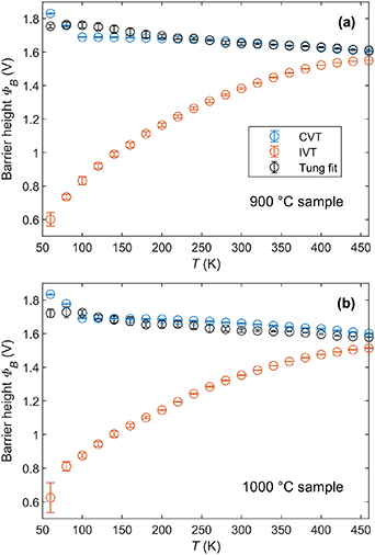
Figure 7 shows a comparison of the SBH using different evaluation methods on the same two heterojunction diodes. Using the fitting model proposed in this paper, the background barrier φB 0 could be evaluated using the measured IVT data at all temperatures, even if strong non-idealities were present. The TE IVT data show strong deviations from the CVT evaluated SBH, whereas the latter show higher values across the whole temperature range, as expected. Only at higher temperatures, they start to approach similar values. This often-seen deviation is due to the current flowing predominantly through the lowest SBHs present at the interface. The SBH evaluated by IVT data is, therefore, reflecting the effective barrier height a device will have in real-world applications, but due to the unknown effective area, this SBH value is rather questionable and not well suited for comparing different Schottky diodes. Although evaluated using completely different methods, the SBHs from CVT measurements and the ones from the IVT data using the fit of the Tung model deviate only by a maximum of 4% across a temperature range of 400 K. This is regarded as a most excellent result given the influence of image force lowering and interface defects to the CV data. In addition, a decrease of about 140 mV in SBH is determined between 60 and 460 K, based on the temperature-related bandgap and Fermi level changes of the two semiconductors, thus providing again confidence for the validity of the used method and the other evaluated parameters. This high degree of agreement also justifies the use of the chosen weight function to account for the weakness of the Tung model to deal with the presence of medium-sized patches.
Figure 7. Comparison of the SBHs gained from IVT data evaluated by thermionic emission theory, IVT data evaluated by the Tung model and by CVT data. Shown are the two representative diodes annealed at (a) 900 °C and (b) 1000 °C.
Download figure:
Standard image High-resolution image
6. Conclusions and outlook
Using the heterojunction p-Si/n-4H-SiC, we were able to realize diodes with a rather high SBH in the range of 1.65 V promising excellent rectifying properties. IVT characterizations in forward direction between 60 and 460 K revealed many nonidealities in the IV curve, especially at lower temperatures. This finding together with the deviation of the extracted SBHs between IVT and CVT indicated the presence of SBH inhomogeneities at the interface. As a consequence, this heterojunction architecture with its rather high SBH is ideal to analyze the influence of patches with low SBH on the device characteristics. Comparisons with theoretical predictions showed at least two separate types of inhomogeneities. Inhomogeneities with a low density and low SBH are assumed to be of predominantly extrinsic source due to e.g. local contaminations. In contrast, inhomogeneities with a higher concentration and a mean SBH around the background SBH are assumed to be of intrinsic source. Tung's model of inhomogeneous SCs was applied to fit the measured data. Depending on the shape of the IV curves, two, or even three Gaussian distributions of SBHs in form of Tung's patch parameter were used for fitting. Due to the relatively large size of the extrinsic patches in combination with the rather high doping level in the depletion layer, the Tung model started to fail at these temperatures. A combination of pinched-off and not pinched-off patches together with a weight function was implemented as a workaround, resulting in excellent fitting results. With this approach, we were able to estimate both the densities and the patch parameters of the different patch distributions as well as to extract physically meaningful values for the background SBH from quite distorted IV curves even at low temperatures. The intrinsic patch densities were found to be about 5.5 × 109 cm−2, whereas the extrinsic densities were orders of magnitudes lower. In case of the diode with three pronounced bumps only 3.5 patches per diode were found to be responsible for the lowest IV bump. The extracted densities can be used as measures to find and reduce low SBH contaminations depending on different process parameters. A comparison with the CVT extracted SBH values gives confidence in the validity of this approach across a wide temperature range of 400 K. In the near future, Schottky-type interfaces with defined, local inhomogeneities generated artificially on SiC substrates with different doping levels and a comparison of the fitted model with BEEM measurements would give more insight in the electrical device performance to verify the validity of the assumptions and approximations made for modeling the experimental data.
Acknowledgments
This work was funded by the Austrian Research Promotion Agency (FFG, Project No. 874907). The authors acknowledge TU Wien University Library for financial support through its Open Access Funding Programme.