Effect of Substrate Holder Design on Stress and Uniformity of Large-Area Polycrystalline Diamond Films Grown by Microwave Plasma-Assisted CVD

 ,
,  ,
,  ,
,
Abstract
:
1. Introduction
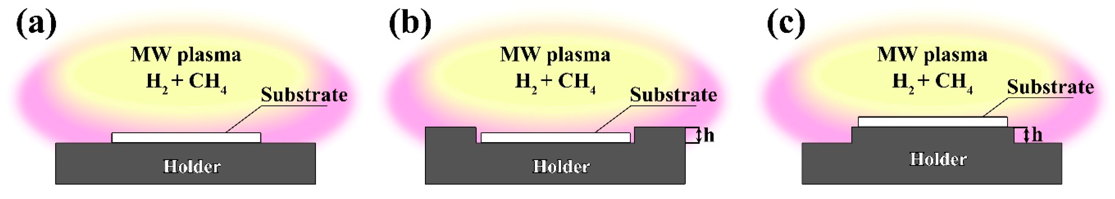
2. Materials and Methods
3. Results
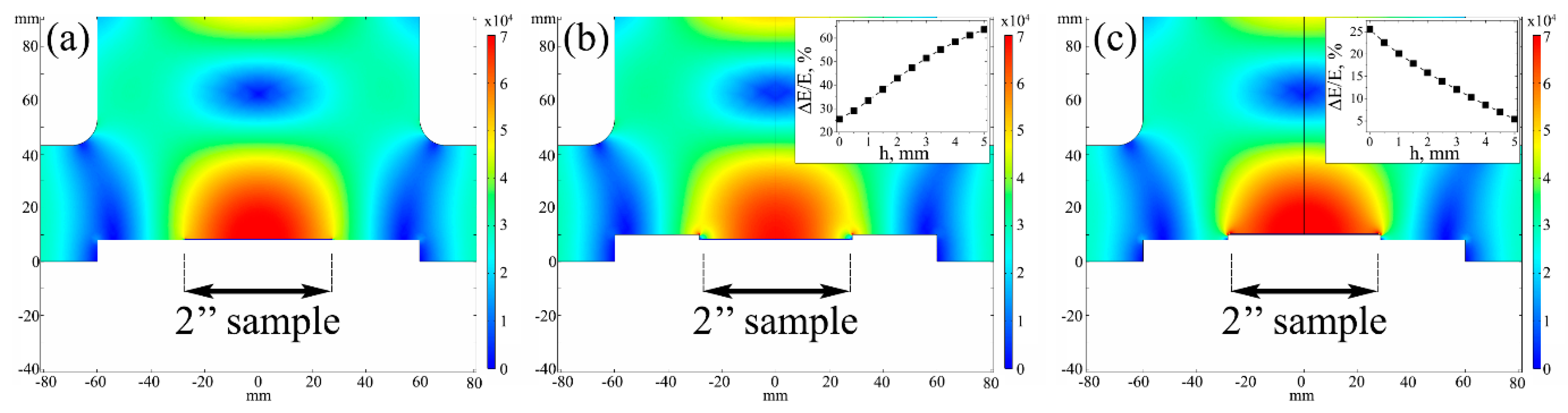
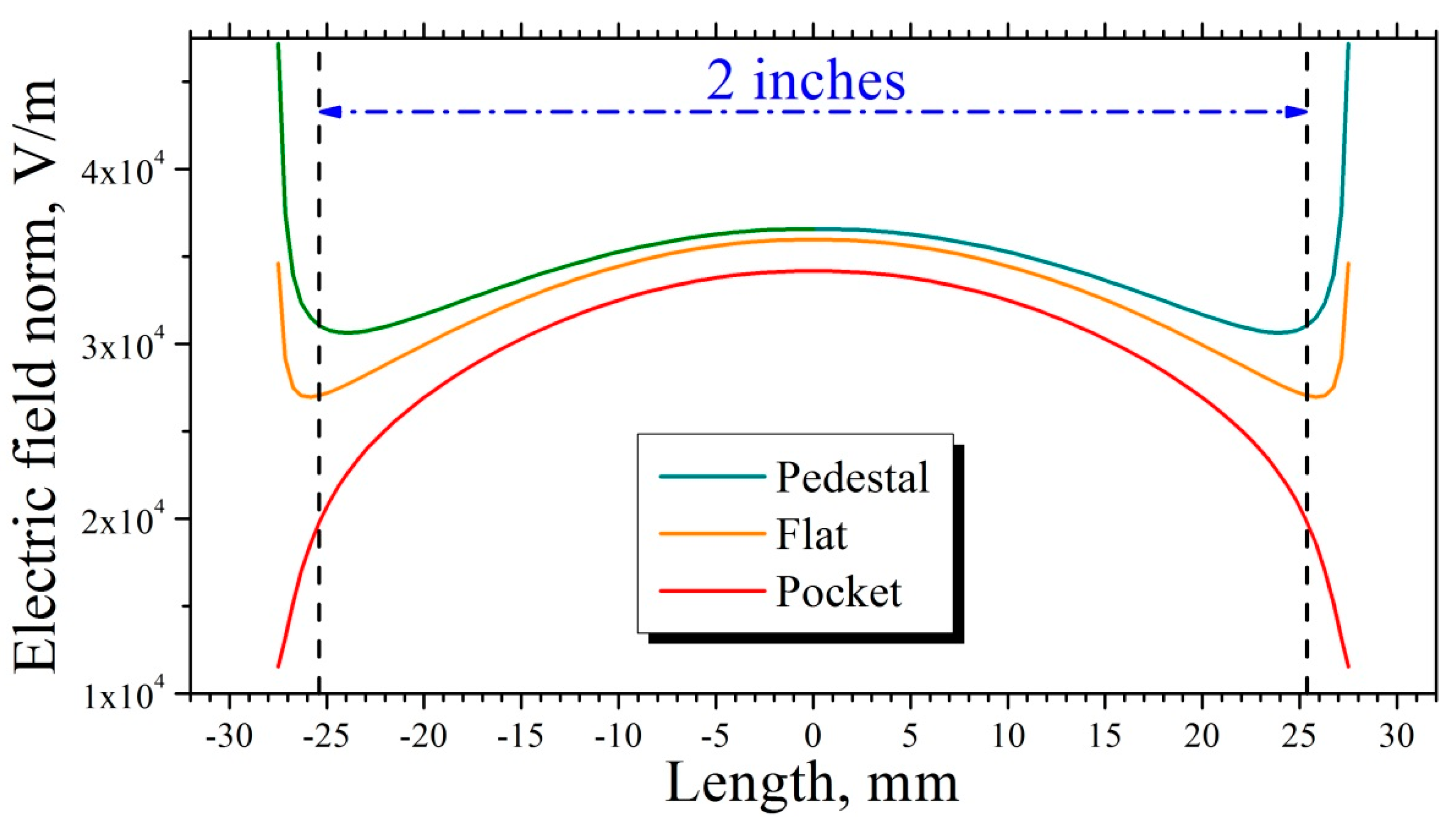
3.1. E-Field Calculations
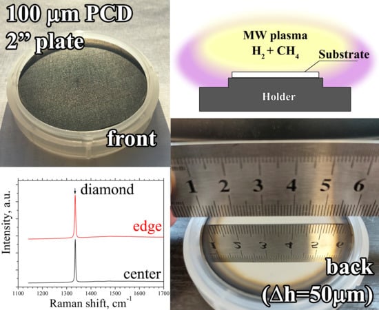
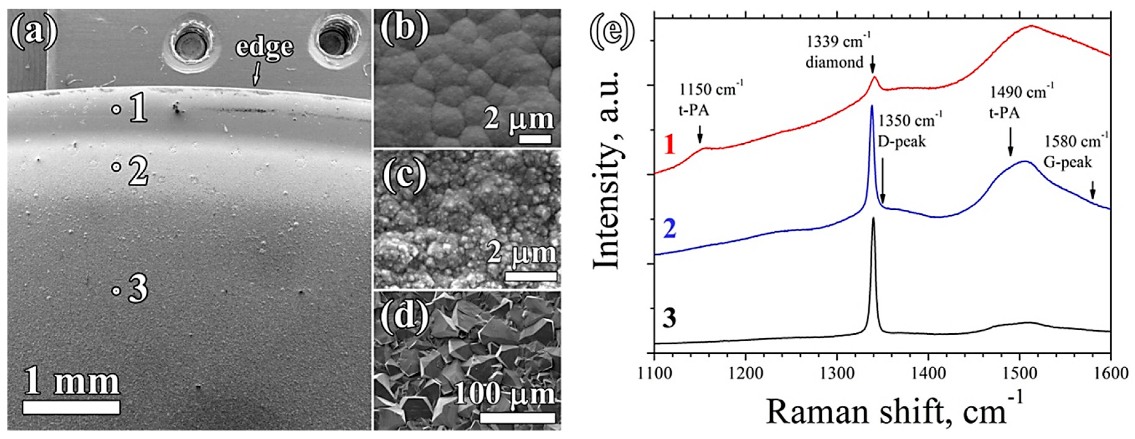
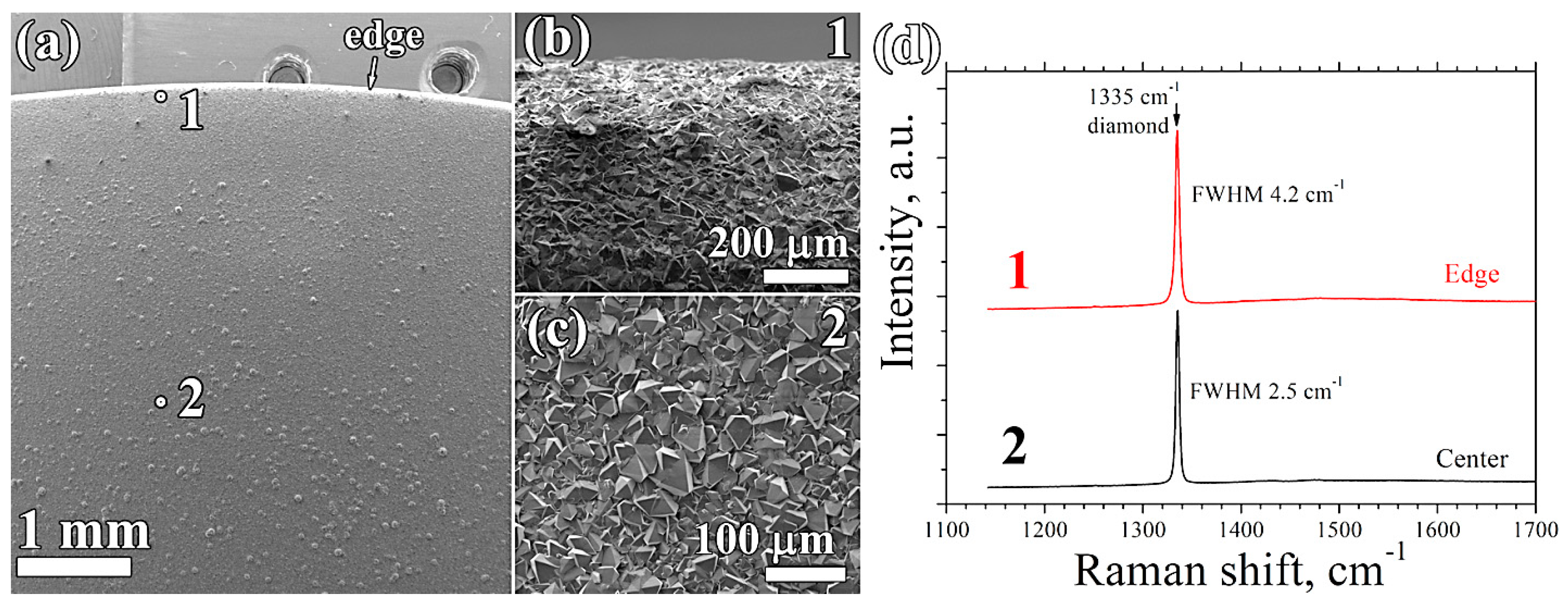
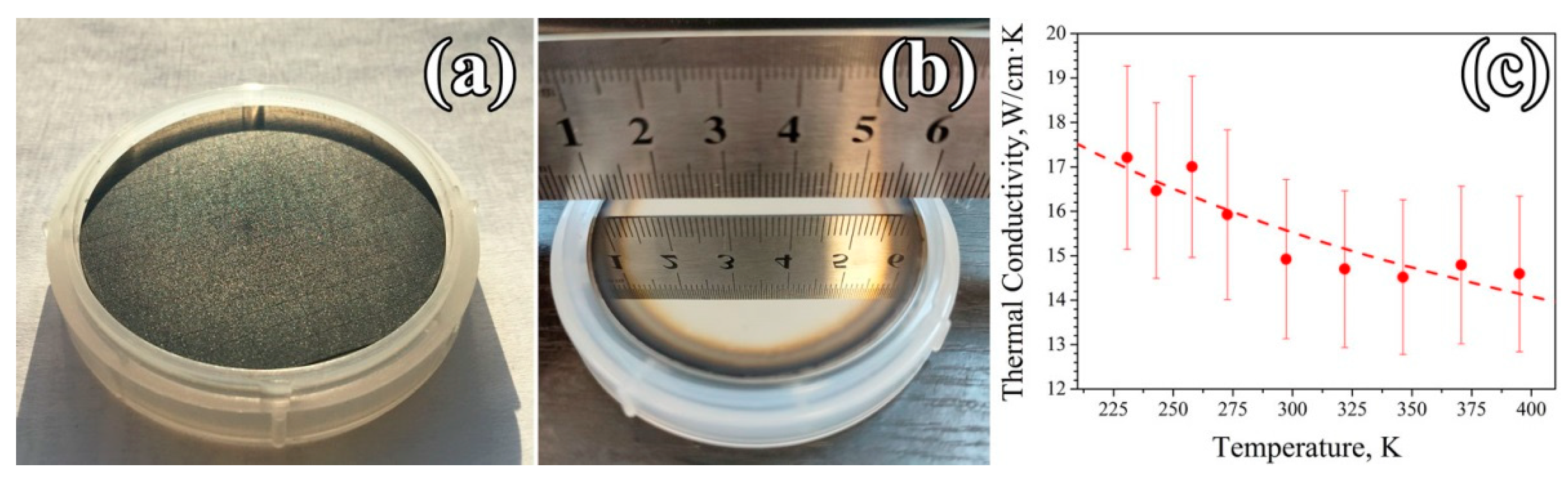
3.2. CVD Synthesis of Thick Diamond Layers
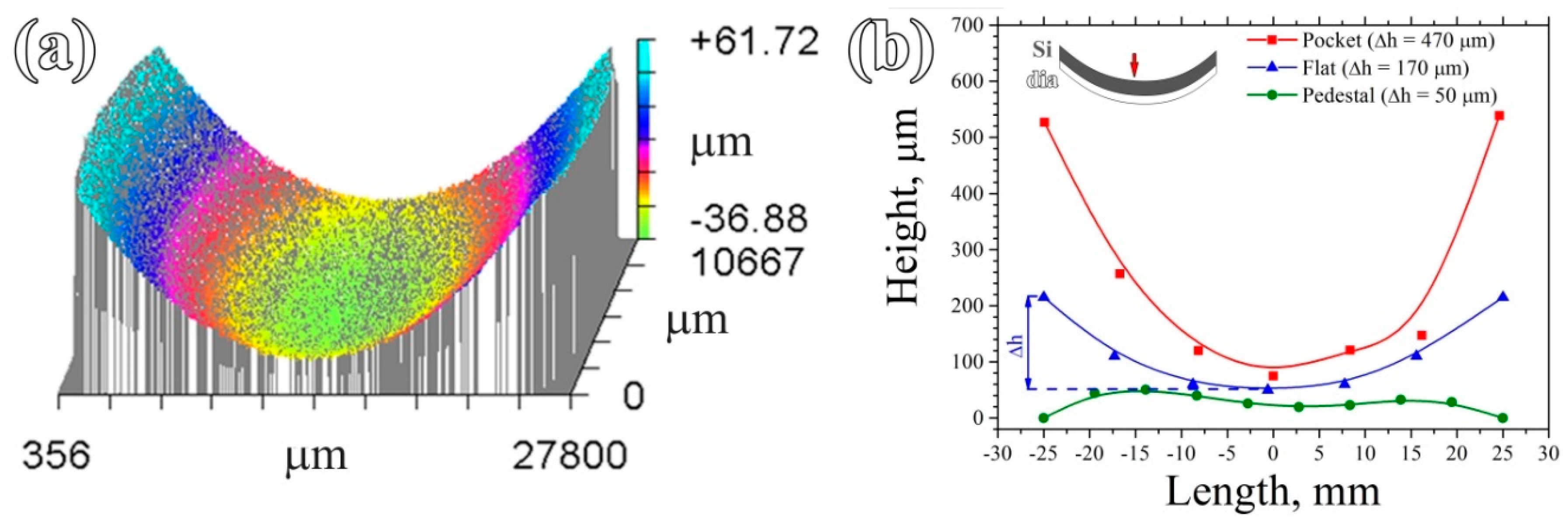
3.3. Bending of the Grown “Diamond-on-Si” Plates
4. Discussion
5. Conclusions
Author Contributions
Funding
Acknowledgments
Conflicts of Interest
References
- Inyushkin, A.V.; Taldenkov, A.N.; Ralchenko, V.G.; Bolshakov, A.P.; Koliadin, A.V.; Katrusha, A.N. Thermal conductivity of high purity synthetic single crystal diamonds. Phys. Rev. B 2018, 97, 144305. [Google Scholar] [CrossRef]
- Hou, G.-Y.; Shu, S.-L.; Feng, J.; Popp, A.; Schmidt, B.; Lu, H.-Y.; Wang, L.-J.; Tian, S.-C.; Tong, C.-Z.; Wang, L.-J. High Power (>27 W) Semiconductor Disk Laser Based on Pre-Metalized Diamond Heat-Spreader. IEEE Photonics J. 2019, 11, 1–8. [Google Scholar] [CrossRef]
- Li, X.; Wang, X.; Li, Y.; Liu, Y. Production and Heat Properties of an X-ray Reflective Anode Based on a Diamond Heat Buffer Layer. Materials 2020, 13, 241. [Google Scholar] [CrossRef] [PubMed] [Green Version]
- Yang, Q.; Zhao, J.; Huang, Y.; Zhu, X.; Fu, W.; Li, C.; Miao, J. A diamond made microchannel heat sink for high-density heat flux dissipation. Appl. Therm. Eng. 2019, 158, 113804. [Google Scholar] [CrossRef]
- Nosaeva, K.; Al-Sawaf, T.; John, W.; Stoppel, D.; Rudolph, M.; Schmückle, F.-J.; Janke, B.; Krüger, O.; Krozer, V.; Heinrich, W.; et al. Multifinger Indium Phosphide Double-Heterostructure Transistor Circuit Technology With Integrated Diamond Heat Sink Layer. IEEE Trans. Electron Devices 2016, 63, 1846–1852. [Google Scholar] [CrossRef]
- Karczemska, A.; Witkowski, D.; Ralchenko, V.; Bolshakov, A.; Sovyk, D.; Lysko, J.; Hassard, J. Diamond Microfluidic Devices manufactured with the replica method. In Proceedings of the 2009 5th International Conference on Perspective Technologies and Methods in MEMS Design, Zakarpattya, Ukraine, 22–24 April 2009; pp. 17–19. [Google Scholar]
- Alcantar-Peña, J.J.; de Obaldia, E.; Tirado, P.; Arellano-Jimenez, M.J.; Ortega Aguilar, J.E.; Veyan, J.F.; Yacaman, M.J.; Koudriavtsev, Y.; Auciello, O. Polycrystalline diamond films with tailored micro/nanostructure/doping for new large area film-based diamond electronics. Diam. Relat. Mater. 2019, 91, 261–271. [Google Scholar] [CrossRef]
- Shikata, S. Single crystal diamond wafers for high power electronics. Diam. Relat. Mater. 2016, 65, 168–175. [Google Scholar] [CrossRef] [Green Version]
- Jagannadham, K. Multilayer diamond heat spreaders for electronic power devices. Solid State Electron. 1998, 42, 2199–2208. [Google Scholar] [CrossRef]
- Tadjer, M.J.; Anderson, T.J.; Hobart, K.D.; Feygelson, T.I.; Caldwell, J.D.; Eddy, C.R.; Kub, F.J.; Butler, J.E.; Pate, B.; Melngailis, J. Reduced Self-Heating in AlGaN/GaN HEMTs Using Nanocrystalline Diamond Heat-Spreading Films. IEEE Electr. Device Lett. 2012, 33, 23–25. [Google Scholar] [CrossRef]
- Amano, H.; Baines, Y.; Beam, E.; Borga, M.; Bouchet, T.; Chalker, P.R.; Charles, M.; Chen, K.J.; Chowdhury, N.; Chu, R.; et al. The 2018 GaN power electronics roadmap. J. Phys. D: Appl. Phys. 2018, 51, 163001. [Google Scholar] [CrossRef]
- Qin, H.; Luan, X.; Feng, C.; Yang, D.; Zhang, G. Mechanical, Thermodynamic and Electronic Properties of Wurtzite and Zinc-Blende GaN Crystals. Materials 2017, 10, 1419. [Google Scholar] [CrossRef] [PubMed] [Green Version]
- Zhou, Y.; Ramaneti, R.; Anaya, J.; Korneychuk, S.; Derluyn, J.; Sun, H.; Pomeroy, J.; Verbeeck, J.; Haenen, K.; Kuball, M. Thermal characterization of polycrystalline diamond thin film heat spreaders grown on GaN HEMTs. Appl. Phys. Lett. 2017, 111, 041901. [Google Scholar] [CrossRef] [Green Version]
- Mu, F.; He, R.; Suga, T. Room temperature GaN-diamond bonding for high-power GaN-on-diamond devices. Scr. Mater. 2018, 150, 148–151. [Google Scholar] [CrossRef]
- Ohki, T.; Yamada, A.; Minoura, Y.; Makiyama, K.; Kotani, J.; Ozaki, S.; Sato, M.; Okamoto, N.; Joshin, K.; Nakamura, N. An over 20-W/mm S-band InAlGaN/GaN HEMT with SiC/diamond-bonded heat spreader. IEEE Electr. Device Lett. 2018, 40, 287–290. [Google Scholar] [CrossRef]
- Schreck, M.; Gsell, S.; Brescia, R.; Fischer, M. Ion bombardment induced buried lateral growth: The key mechanism for the synthesis of single crystal diamond wafers. Sci. Rep. 2017, 7, 44462. [Google Scholar] [CrossRef]
- Gallheber, B.-C.; Fischer, M.; Mayr, M.; Straub, J.; Schreck, M. Growth, stress, and defects of heteroepitaxial diamond on Ir/YSZ/Si(111). J. Appl. Phys. 2018, 123, 225302. [Google Scholar] [CrossRef]
- Anaya, J.; Bai, T.; Wang, Y.; Li, C.; Goorsky, M.; Bougher, T.L.; Yates, L.; Cheng, Z.; Graham, S.; Hobart, K.D.; et al. Simultaneous determination of the lattice thermal conductivity and grain/grain thermal resistance in polycrystalline diamond. Acta Mater. 2017, 139, 215–225. [Google Scholar] [CrossRef]
- Wort, C.J.H.; Sweeney, C.G.; Cooper, M.A.; Scarsbrook, G.A.; Sussmann, R.S. Thermal properties of bulk polycrystalline CVD diamond. Diam. Relat. Mater. 1994, 3, 1158–1167. [Google Scholar] [CrossRef]
- Hartmann, J.; Voigt, P.; Reichling, M. Measuring local thermal conductivity in polycrystalline diamond with a high resolution photothermal microscope. J. Appl. Phys. 1997, 81, 2966–2972. [Google Scholar] [CrossRef]
- Popovich, A.F.; Ralchenko, V.G.; Balla, V.K.; Mallik, A.K.; Khomich, A.A.; Bolshakov, A.P.; Sovyk, D.N.; Ashkinazi, E.E.; Yurov, V.Y. Growth of 4 ″diameter polycrystalline diamond wafers with high thermal conductivity by 915 MHz microwave plasma chemical vapor deposition. Plasma Sci. Technol. 2017, 19, 035503. [Google Scholar] [CrossRef]
- Bolshakov, A.P.; Ralchenko, V.G.; Yurov, V.Y.; Shu, G.; Bushuev, E.V.; Khomich, A.A.; Ashkinazi, E.E.; Sovyk, D.N.; Antonova, I.A.; Savin, S.S.; et al. Enhanced deposition rate of polycrystalline CVD diamond at high microwave power densities. Diam. Relat. Mater. 2019, 97, 107466. [Google Scholar] [CrossRef]
- Ralchenko, V.G.; Smolin, A.A.; Konov, V.I.; Sergeichev, K.F.; Sychov, I.A.; Vlasov, I.I.; Migulin, V.V.; Voronina, S.V.; Khomich, A.V. Large-area diamond deposition by microwave plasma. Diam. Relat. Mater. 1997, 6, 417–421. [Google Scholar] [CrossRef]
- Sedov, V.S.; Voronin, A.A.; Komlenok, M.S.; Savin, S.S.; Martyanov, A.K.; Popovich, A.F.; Altakhov, A.S.; Kurochka, A.S.; Markus, D.V.; Ralchenko, V.G. Laser-Assisted Formation of High-Quality Polycrystalline Diamond Membranes. Jo.Russ. Laser Res. 2020. [Google Scholar] [CrossRef]
- Handbook of Industrial Diamonds and Diamond Films, 1st ed.; Prelas, M.A. (Ed.) CRC Press: Boca Raton, FL, USA, 2018. [Google Scholar]
- Su, J.J.; Li, Y.F.; Li, X.L.; Yao, P.L.; Liu, Y.Q.; Ding, M.H.; Tang, W.Z. A novel microwave plasma reactor with a unique structure for chemical vapor deposition of diamond films. Diam. Relat. Mater. 2014, 42, 28–32. [Google Scholar] [CrossRef]
- Zvanya, J.; Holber, W.; Cullen, C.; Morris, T.; Basnett, A.; Basnett, R.; Hettinger, J.; Krchnavek, R.R. Toroidal plasma enhanced CVD of diamond films. J. Vac. Sci. Technol. A 2014, 32, 050605. [Google Scholar] [CrossRef]
- Harada, Y.; Hishinuma, R.; Spătaru, N.; Sakurai, Y.; Miyasaka, K.; Terashima, C.; Uetsuka, H.; Suzuki, N.; Fujishima, A.; Kondo, T.; et al. High-speed synthesis of heavily boron-doped diamond films by in-liquid microwave plasma CVD. Diam. Relat. Mater. 2019, 92, 41–46. [Google Scholar] [CrossRef]
- Vikharev, A.L.; Gorbachev, A.M.; Lobaev, M.A.; Muchnikov, A.B.; Radishev, D.B.; Isaev, V.A.; Chernov, V.V.; Bogdanov, S.A.; Drozdov, M.N.; Butler, J.E. Novel microwave plasma-assisted CVD reactor for diamond delta doping. Phys. Status Solidi Rapid Res. Lett. 2016, 10, 324–327. [Google Scholar] [CrossRef]
- Geis, M.W.; Wade, T.C.; Wuorio, C.H.; Fedynyshyn, T.H.; Duncan, B.; Plaut, M.E.; Varghese, J.O.; Warnock, S.M.; Vitale, S.A.; Hollis, M.A. Progress Toward Diamond Power Field-Effect Transistors. Phys. Status Solidi A 2018, 215, 1800681. [Google Scholar] [CrossRef]
- Widmann, C.J.; Müller-Sebert, W.; Lang, N.; Nebel, C.E. Homoepitaxial growth of single crystalline CVD-diamond. Diam. Relat. Mater. 2016, 64, 1–7. [Google Scholar] [CrossRef]
- Lobaev, M.A.; Gorbachev, A.M.; Vikharev, A.L.; Isaev, V.A.; Radishev, D.B.; Bogdanov, S.A.; Drozdov, M.N.; Yunin, P.A.; Butler, J.E. Investigation of boron incorporation in delta doped diamond layers by secondary ion mass spectrometry. Thin Solid Films 2018, 653, 215–222. [Google Scholar] [CrossRef]
- Bolshakov, A.P.; Ralchenko, V.G.; Yurov, V.Y.; Popovich, A.F.; Antonova, I.A.; Khomich, A.A.; Ashkinazi, E.E.; Ryzhkov, S.G.; Vlasov, A.V.; Khomich, A.V. High-rate growth of single crystal diamond in microwave plasma in CH4/H2 and CH4/H2/Ar gas mixtures in presence of intensive soot formation. Diam. Relat. Mater. 2016, 62, 49–57. [Google Scholar] [CrossRef]
- Nad, S.; Asmussen, J. Analyses of single crystal diamond substrates grown in a pocket substrate holder via MPACVD. Diam. Relat. Mater. 2016, 66, 36–46. [Google Scholar] [CrossRef]
- Charris, A.; Nad, S.; Asmussen, J. Exploring constant substrate temperature and constant high pressure SCD growth using variable pocket holder depths. Diam. Relat. Mater. 2017, 76, 58–67. [Google Scholar] [CrossRef]
- Schreck, M.; Asmussen, J.; Shikata, S.; Arnault, J.-C.; Fujimori, N. Large-area high-quality single crystal diamond. MRS Bull. 2014, 39, 504–510. [Google Scholar] [CrossRef]
- Yang, B.; Shen, Q.; Gan, Z.; Liu, S. Analysis of improving the edge quality and growth rate of single-crystal diamond growth using a substrate holder. CrystEngComm 2019, 21, 6574–6584. [Google Scholar] [CrossRef]
- Ashkihazi, E.E.; Sedov, V.S.; Sovyk, D.N.; Khomich, A.A.; Bolshakov, A.P.; Ryzhkov, S.G.; Khomich, A.V.; Vinogradov, D.V.; Ralchenko, V.G.; Konov, V.I. Plateholder design for deposition of uniform diamond coatings on WC-Co substrates by microwave plasma CVD for efficient turning application. Diam. Relat. Mater. 2017, 75, 169–175. [Google Scholar] [CrossRef]
- Sedov, V.S.; Khomich, A.A.; Ralchenko, V.G.; Martyanov, A.K.; Savin, S.S.; Poklonskaya, O.N.; Trofimov, N.S. Growth of Si-Doped Polycrystalline Diamond Films on AlN Substrates by Microwave Plasma Chemical Vapor Deposition. J. Coat. Sci. Technol. 2015, 2, 38–45. [Google Scholar] [CrossRef]
- Sukhadolau, A.V.; Ivakin, E.V.; Ralchenko, V.G.; Khomich, A.V.; Vlasov, A.V.; Popovich, A.F. Thermal conductivity of CVD diamond at elevated temperatures. Diam. Relat. Mater. 2005, 14, 589–593. [Google Scholar] [CrossRef]
- Mankelevich, Y.A.; May, P.W. New insights into the mechanism of CVD diamond growth: Single crystal diamond in MW PECVD reactors. Diam. Relat. Mater. 2008, 17, 1021–1028. [Google Scholar] [CrossRef]
- Mahoney, E.J.D.; Rodriguez, B.J.; Mushtaq, S.; Truscott, B.S.; Ashfold, M.N.R.; Mankelevich, Y.A. Imaging and Modeling the Optical Emission from CH Radicals in Microwave Activated C/H Plasmas. J. Phys. Chem. A 2019, 123, 9966–9977. [Google Scholar] [CrossRef]
- Sedov, V.; Ralchenko, V.; Khomich, A.A.; Vlasov, I.; Vul, A.; Savin, S.; Goryachev, A.; Konov, V. Si-doped nano- and microcrystalline diamond films with controlled bright photoluminescence of silicon-vacancy color centers. Diam. Relat. Mater. 2015, 56, 23–28. [Google Scholar] [CrossRef]
- Podgursky, V.; Bogatov, A.; Sedov, V.; Sildos, I.; Mere, A.; Viljus, M.; Buijnsters, J.G.; Ralchenko, V. Growth dynamics of nanocrystalline diamond films produced by microwave plasma enhanced chemical vapor deposition in methane/hydrogen/air mixture: Scaling analysis of surface morphology. Diam. Relat. Mater. 2015, 58, 172–179. [Google Scholar] [CrossRef]
- Ashkinazi, E.E.; Khmelnitskii, R.A.; Sedov, V.S.; Khomich, A.A.; Khomich, A.V.; Ralchenko, V.G. Morphology of Diamond Layers Grown on Different Facets of Single Crystal Diamond Substrates by a Microwave Plasma CVD in CH4-H2-N2 Gas Mixtures. Crystals 2017, 7, 166. [Google Scholar] [CrossRef] [Green Version]
- Ager, J.W. Residual Stress in Diamond and Amorphous Carbon Films. MRS Online Proc. Libr. Arch. 1995, 383. [Google Scholar] [CrossRef]
- Gaydaychuk, A.; Zenkin, S.; Linnik, S. Influence of Al-Si-N interlayer on residual stress of CVD diamond coatings. Surf. Coat. Technol. 2019, 357, 348–352. [Google Scholar] [CrossRef]


© 2020 by the authors. Licensee MDPI, Basel, Switzerland. This article is an open access article distributed under the terms and conditions of the Creative Commons Attribution (CC BY) license (http://creativecommons.org/licenses/by/4.0/).
Share and Cite
Sedov, V.; Martyanov, A.; Altakhov, A.; Popovich, A.; Shevchenko, M.; Savin, S.; Zavedeev, E.; Zanaveskin, M.; Sinogeykin, A.; Ralchenko, V.; et al. Effect of Substrate Holder Design on Stress and Uniformity of Large-Area Polycrystalline Diamond Films Grown by Microwave Plasma-Assisted CVD. Coatings 2020, 10, 939. https://doi.org/10.3390/coatings10100939
Sedov V, Martyanov A, Altakhov A, Popovich A, Shevchenko M, Savin S, Zavedeev E, Zanaveskin M, Sinogeykin A, Ralchenko V, et al. Effect of Substrate Holder Design on Stress and Uniformity of Large-Area Polycrystalline Diamond Films Grown by Microwave Plasma-Assisted CVD. Coatings. 2020; 10(10):939. https://doi.org/10.3390/coatings10100939
Chicago/Turabian StyleSedov, Vadim, Artem Martyanov, Alexandr Altakhov, Alexey Popovich, Mikhail Shevchenko, Sergey Savin, Evgeny Zavedeev, Maxim Zanaveskin, Andrey Sinogeykin, Victor Ralchenko, and et al. 2020. "Effect of Substrate Holder Design on Stress and Uniformity of Large-Area Polycrystalline Diamond Films Grown by Microwave Plasma-Assisted CVD" Coatings 10, no. 10: 939. https://doi.org/10.3390/coatings10100939