
Abstract
A hybrid plasmonic waveguide device was designed using a trench structure. This waveguide device was designed to improve the affinity of plasmonic devices with optical circuits by connecting them with traditional waveguide structures. The waveguide device consists of three structural segments, comprising two traditional waveguide sections for input and transmission and a hybrid plasmonic waveguide. The designed waveguide structure was evaluated using numerical analysis techniques such as the finite-difference time-domain method. The device's transmission property affects the interference between the guided light and the surface plasmon polaritons. Controlling the length of the hybrid waveguide device, which is composed of a traditional waveguide coated with a gold layer, allows the transmission intensity of the device to be controlled. The device's transmission characteristic can be controlled based on the relationship between the wavelength of the incident light and the length of the hybrid waveguide device. The device will transmit only specific incident light wavelengths because the length of the hybrid plasmonic waveguide remains constant. The characteristics of this device indicate potential for applications to nanoscale devices, optical integrated circuits and plasmonic sensors.
Export citation and abstract BibTeX RIS

Original content from this work may be used under the terms of the Creative Commons Attribution 4.0 licence. Any further distribution of this work must maintain attribution to the author(s) and the title of the work, journal citation and DOI.
1. Introduction
In recent years, communications networks have shown a trend for rapidly increasing traffic. To cope with this problem, the capacities of optical networks have been increased, but because of the diffraction limit of light, it is difficult to integrate the very large optical devices required with the comparatively small electronic devices used in these networks. Therefore, surface plasmon polaritons (SPPs), which are converted from light energy and have no diffraction limit, have been attracting attention for use in communications applications [1, 2]. To realize integrated circuits that can incorporate SPPs, several device structures based on use of SPPs, which are known as plasmonic devices, have been proposed by various research groups [3–8]. As input and output methods for the plasmonic devices reported to date, gratings and the end-fire coupling method are commonly used [9, 10]. The methods that use gratings require large areas and offer low coupling efficiency. Although the end-fire coupling method provides high coupling efficiency, the plasmonic waveguide is required to be accessible at the edge of the circuit. Therefore, both of these methods are difficult to use in integrated circuits in practice. Plasmonic devices for use in integrated circuits that incorporate SPPs must couple the SPPs from light propagating in an optical waveguide. Therefore, numerous coupler structures have been reported that use waveguides between the light and the SPPs [11–14]. The coupling methods used in these structures include butt coupling and evanescent coupling [15–18]. However, these structures are not easy to fabricate as designed [19]. Several hybrid plasmonic devices that couple SPPs from light propagating in optical waveguides have also been reported [20–23]. These structures give the devices low loss and compact size characteristics.
In this paper, we design a hybrid plasmonic waveguide device to couple propagating light from a traditional waveguide to produce SPPs using a trench structure. The device has a simple structure and improves the affinity with the optical circuit by connecting to the traditional waveguide. Part of the traditional waveguide is coated with gold in the proposed structure. The portion of the waveguide with the gold coating is a hybrid plasmonic waveguide composed of both traditional and plasmonic waveguides. We intend to use silicon-on-insulator (SOI) technology to fabricate the designed structure in future work. It is assumed that electron beam lithography will be used as part of the fabrication method for the proposed structure. The structure is designed in this work using the finite-difference time-domain (FDTD) method. We use the FDTD method software package MIT Electromagnetic equation Propagation (MEEP) [24], which is popular among research groups for use in numerical research on plasmonics [25, 26].
2. Design of the hybrid plasmonic waveguide device
Schematics of the device structure are presented in figure 1. Figure 1(a) shows the x-y plane view of the structure. Figure 1(b) shows the y-z plane view. Figure 1(c) shows the three-dimensional view of the structure. The substrate is composed of silicon. A silicon dioxide layer with a thickness of 1.0 μm lies on top of this silicon substrate. The device structure is then fabricated on the silicon dioxide membrane. The core of the traditional waveguide is composed of silicon. The width and height of the waveguide are denoted by w and t, respectively. Part of the traditional waveguide was then coated with gold using the evaporation method. We selected gold as the coating metal because gold is a low-loss material in the infrared light wavelength range and is also less susceptible to oxidation than other metals [27, 28]. The thickness of this gold layer is 100 nm. The length of the evaporated gold segment is denoted by Lg . w is set at 500 nm.
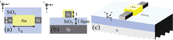
Figure 1. Schematics of the hybrid plasmonic waveguide device structure, showing (a) the x-y plane view, (b) the y-z plane view, and (c) the three-dimensional view.
Download figure:
Standard image High-resolution imageTo design t for the waveguide device, we calculated both the effective refractive index of the waveguide and the propagation length as functions of t. The SPP mode in the plasmonic waveguide was analyzed using the approach given in [29, 30]. In the analysis, the effective refractive index of the waveguide and the propagation length were determined [31]. The values of the effective refractive index of the waveguide and the propagation length were calculated using Scilab, which is a free open-source software package. Figure 2(a) shows the effective refractive indices of both the traditional waveguide and the plasmonic waveguide as functions of t. The wavelength of the incident light is 1300 nm. The size of the designed structure decreases when the incident light wavelength decreases. Therefore, we adopted the incident light wavelength of 1300 nm rather than the wavelength of 1550 nm. The open circles and closed circles in the figure represent the effective refractive indices of the fundamental mode and the first-order mode of the plasmonic waveguide, respectively. The open triangles and closed triangles in the figure represent the refractive indices of the fundamental mode and the first-order mode of the traditional waveguide, respectively. Figure 2(b) shows the propagation length of the plasmonic waveguide as a function of t. The open circles and closed circles represent the propagation lengths of the fundamental mode and the first-order mode of the plasmonic waveguide, respectively. The propagation length of the fundamental mode decreases sharply when t increases from 75 to 100 nm. When t increases from 100 to 1000 nm, the propagation length of the fundamental mode increases in tandem from 5 to 30 μm. Similarly, the propagation length of the first-order mode decreases sharply when t increases from 270 to 300 nm. When t increases from 300 to 1000 nm, the propagation length of the fundamental mode increases in tandem from 5 to 25 μm. To reduce their losses, the plasmonic and traditional waveguides must be designed to become a single mode waveguide. Therefore, t is set at 300 nm. The effective refractive indices of the plasmonic and traditional waveguides are then 3.20 and 2.89, respectively. The designed structure was compared with other hybrid plasmonic waveguides from the literature. Table 1 presents the comparison results in terms of fabrication complexity and coupler size. The proposed structure is characterized by its simple shape and small coupler size.

Figure 2. (a) Effective refractive indices of the traditional waveguide and the plasmonic waveguide as functions of t. w is set at 500 nm. The wavelength of the incident light is 1300 nm. The open circles and closed circles represent the effective refractive indices of the fundamental mode and the first-order mode of the plasmonic waveguide, respectively. The open triangles and closed triangles represent the refractive indices of the fundamental mode and the first-order mode of the traditional waveguide, respectively. (b) Propagation lengths of the plasmonic waveguide as functions of t. The open circles and closed circles represent the propagation lengths of the fundamental mode and the first-order mode of the plasmonic waveguide, respectively.
Download figure:
Standard image High-resolution imageTable 1. Comparison results for hybrid waveguide structure shape and coupler size.
| Structure | Structure shape | Coupler size |
|---|---|---|
| Polarization-independent | Double cylindrical waveguides | 4.25 μm |
| directional coupler [32] | ||
| Hybrid plasmonic coupler [19] | Double rectangular waveguides (SOI) | Several μm |
| Silicon-based hybrid | Single waveguide (SOI) | Several μm |
| plasmonic waveguide [33] | that requires a triangular structure | |
| Proposed structure | Single rectangular waveguide (SOI) | Less than 2 μm |
3. Characteristics of the hybrid plasmonic waveguide device
The waveguide device was designed to include three structural segments, including traditional waveguide sections for input and transmission and a hybrid plasmonic waveguide. The cores of the traditional waveguide segments used for input and transmission both supported guided light propagation. The portion of the hybrid plasmonic waveguide segment that was covered by the gold layer supported the propagation of both guided light and SPPs. The guided light in the traditional waveguide segments was coupled to the SPPs in the hybrid plasmonic waveguide segment. Figure 3 shows the characteristics of the coupling loss between the traditional waveguide segments and the hybrid plasmonic waveguide segment. The coupling loss was calculated to be approximately −1.0 dB at the incident light wavelengths around 1300 nm. When the guided light is coupled to the SPPs, interference between the guided light and the SPPs is induced in the hybrid plasmonic waveguide segment. To determine Lg , the beat length of the interference between the guided light and the SPPs must be evaluated. The beat length is calculated using [34]

where LB , βp , and βt denote the beat length of the interference between the SPPs and the guided light and the propagation constants of the SPPs and the guided light, respectively. The beat length of the designed waveguide was calculated using equation (1) to be 2100 nm. Figure 4 shows the electric field intensity profiles at the center of the waveguide device in the designed structure with (a) Lg = 1600 nm and (b) Lg = 2100 nm. The wavelength of the incident light is 1300 nm. The incident light has an electric field component in the y direction. w and t are set at 500 and 300 nm, respectively. In figure 4(a), the interference between the guided light and the SPPs in the hybrid plasmonic waveguide segment is shown to affect the transmission behavior of the device. The interference between the guided light and the SPPs induces self-imaging [10, 34, 35] in the hybrid plasmonic waveguide segment. The electric field intensity profile of the hybrid plasmonic waveguide segment, which is induced by the interference, shifts toward both sides at the edge of the gold layer. The SPPs are reflected at the edge of the gold layer. Therefore, at Lg = 1600 nm, the transmission of the device decreases. In contrast, at Lg = 2100 nm, the electric field intensity profile of the hybrid plasmonic waveguide segment shifts toward the center of the device at the edge of the gold layer. This means that the guided light can propagate into the traditional waveguide segment for transmission. Therefore, the transmission of the device increases in this case. These results show that the device's transmission intensity can be controlled using Lg . Figure 5 shows the transmission intensities as functions of the incident light wavelength. w and t are set at 500 and 300 nm, respectively. The broken and solid lines represent the transmission intensities with the Lg values of 1600 and 2100 nm, respectively. The transmission intensity is set at 0 dB when the transmission is equivalent to the transmission of the structure without the hybrid plasmonic waveguide segment, i.e., Lg = 0 nm. Transmission at the wavelength of 1300 nm decreases when Lg is 1600 nm. This is because the self-image of the electric field profile induced by the interference between the guided light and the SPPs cannot be coupled to the traditional waveguide segment. The troughs in the transmission intensities with the Lg values of 1600 and 2100 nm are −11 dB at the wavelength of 1303 nm and −9 dB at the wavelength of 1265 nm, respectively. The guided light intensity in the traditional waveguide segment used for input is coupled to the hybrid plasmonic waveguide segment and decreases after propagation over a distance Lg of 1600 nm at the wavelength of 1300 nm. Change in the incident light wavelength also causes a change in LB . This change in LB then affects the self-imaging that occurs in the hybrid plasmonic waveguide segment. Therefore, the transmission intensity changes when the incident light wavelength changes. The device's transmission characteristic can be controlled based on the relationship between the incident light wavelength and Lg . The device can transmit incident light at a specific wavelength because Lg is constant. Lg thus affects the characteristics of the structure strongly. It would be difficult to fabricate the structure with Lg as the designed length. To investigate the effects of structural parameter variations, we analyzed the transmission intensities with Lg ranging from 1560 to 1640 nm. The variation in Lg ranged from 1560 to 1640 nm with steps of 40 nm. Figure 6 shows the transmission intensities as functions of the incident light wavelength with Lg ranging from 1560 to 1640 nm. The troughs in the transmission intensities with the Lg values of 1560, 1600, and 1640 nm are −9 dB at the wavelength of 1294 nm, −11 dB at the wavelength of 1303 nm, and −12 dB at the wavelength of 1314 nm, respectively. The investigation showed that the transmission intensity changed by 1 to 2 dB and the trough wavelength changed by 10 nm in the case where Lg deviated by only 40 nm. Therefore, Lg must be fabricated with a length close to the designed length. Furthermore, the transmission intensity of the proposed structure could be influenced by the thickness of the gold layer of the hybrid plasmonic waveguide. Therefore, we investigated the relationship between the transmission intensity and the gold layer thickness. We designed the hybrid plasmonic waveguide with a gold layer thickness of 100 nm. To investigate the relationship between the transmission intensity and the gold layer thickness, we analyzed the transmission intensity at gold thicknesses of 50, 100, and 200 nm. Figure 7 shows the transmission intensities as functions of the incident light wavelength with gold layer thicknesses of 50, 100, and 200 nm. The troughs in the transmission intensities for the gold layer thicknesses of 50, 100, and 200 nm are −12 dB at the wavelength of 1309 nm, −11 dB at the wavelength of 1303 nm, and −10 dB at the wavelength of 1302 nm, respectively. The results show that gold layer thickness of the hybrid plasmonic waveguide affected the transmission intensity only slightly. The transmission intensity changed by 1 to 2 dB and the trough wavelength changed by several nm when the gold layer thickness changed from 50 to 200 nm.
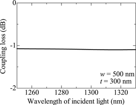
Figure 3. Coupling loss between the traditional waveguide segments and the hybrid plasmonic waveguide segment around 1300 nm.
Download figure:
Standard image High-resolution image
Figure 4. Profiles of the electric field intensity at the center of the waveguide device in the designed structure with (a) Lg = 1600 nm and (b) Lg = 2100 nm. The incident light wavelength is 1300 nm. The incident light has an electric field component in the y direction. w and t are set at 500 and 300 nm, respectively.
Download figure:
Standard image High-resolution image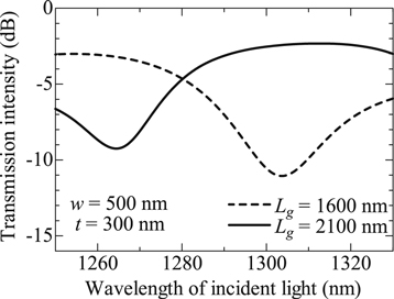
Figure 5. Transmission intensities as functions of the incident light wavelength. The broken and solid lines correspond to the transmission intensities for the Lg values of 1600 and 2100 nm, respectively.
Download figure:
Standard image High-resolution image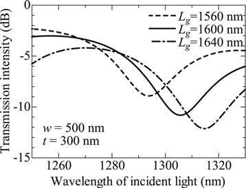
Figure 6. Transmission intensities as functions of the incident light wavelength with Lg varying from 1560 to 1640 nm.
Download figure:
Standard image High-resolution image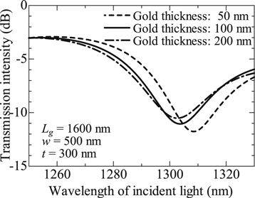
Figure 7. Transmission intensities as functions of the incident light wavelength with gold layer thicknesses of 50, 100, and 200 nm.
Download figure:
Standard image High-resolution image
4. Conclusion
We have designed a hybrid plasmonic waveguide device using a trench structure. The width and height of the waveguide were set at 500 and 300 nm, respectively. Part of the waveguide structure was coated with a gold layer. The segment of the waveguide that was covered with this gold layer forms a hybrid plasmonic waveguide that can support the propagation of both guided light and SPPs. The interference between the guided light and the SPPs affects the device's transmission intensity. The device transmission intensity can thus be controlled based on the length of the hybrid plasmonic waveguide. Different hybrid plasmonic waveguide lengths therefore lead to different transmission characteristics for the device. The device would only transmit incident light at a specific wavelength. The designed hybrid plasmonic waveguide device has a simple structure and improves the device affinity with the optical circuit by connecting it to traditional waveguides. These characteristics of the designed waveguide device thus make it suitable for application to nanoscale devices, optical integrated circuits, and plasmonic sensors.
Acknowledgments
Part of this research was supported by JSPS KAKENHI under Grant Number 17K06376 and the Support Center for Advanced Telecommunications Technology Research Foundation (SCAT). We thank David MacDonald, MSc, from Edanz Group (https://en-author-services.edanzgroup.com/ac) for editing a draft of this manuscript.