
Abstract
Over the past decade, the global cumulative installed photovoltaic (PV) capacity has grown exponentially, reaching 591 GW in 2019. Rapid progress was driven in large part by improvements in solar cell and module efficiencies, reduction in manufacturing costs and the realization of levelized costs of electricity that are now generally less than other energy sources and approaching similar costs with storage included. Given this success, it is a particularly fitting time to assess the state of the photovoltaics field and the technology milestones that must be achieved to maximize future impact and forward momentum. This roadmap outlines the critical areas of development in all of the major PV conversion technologies, advances needed to enable terawatt-scale PV installation, and cross-cutting topics on reliability, characterization, and applications. Each perspective provides a status update, summarizes the limiting immediate and long-term technical challenges and highlights breakthroughs that are needed to address them. In total, this roadmap is intended to guide researchers, funding agencies and industry in identifying the areas of development that will have the most impact on PV technology in the upcoming years.
Export citation and abstract BibTeX RIS

Original content from this work may be used under the terms of the Creative Commons Attribution 4.0 license. Any further distribution of this work must maintain attribution to the author(s) and the title of the work, journal citation and DOI.
Table of acronyms
| AFM | Atomic force microscopy |
| Al-BSF | Aluminum back surface field |
| ALT | Accelerated lifetime testing |
| APT | Atom probe tomoography |
| APV | Agrivoltaics |
| BIPV | Building-integrated photovoltaics |
| CEC | Commission of European Communities |
| CIGS | Group I-III-VI chalcopyrite (Ag,Cu)(In,Ga)(S,Se)2 semiconductor alloys |
| DL | Direct labor |
| EBSD | Electron backscatter diffraction |
| EELS | Electron energy-loss spectroscopy |
| ELO | Epitaxial liftoff |
| HALE | High-altitude long-endurance |
| HVPE | Hydride vapor phase epitaxy |
| IBC | Interdigitated back contact |
| IEC | International Electrotechnical Commission |
| IRENA | International Renewable Energy Agency |
| I-V | Current-voltage |
| LCOE | Levelized cost of energy |
| LeTID | Light and elevated temperature induced degradation |
| LID | Light-induced degradation |
| MHP | Metal halide perovskite |
| MOVPE | Metalorganic vapor phase epitaxy |
| PERC | Passivated emitter and rear cell |
| PID | Potential-induced degradation |
| PSC | Perovskite solar cells |
| PV | Photovoltaic |
| QFLS | Quasi-Fermi level splitting |
| SAS | Sulfurization-after-selenization |
| SEM | Scanning electron microscopy |
| SHJ | Silicon hetero-junction |
| spiro-O-MeTAD | 2,2',7,7'-Tetrakis[N,N-di(4-methoxyphenyl)amino]-9,9'-spirobifluorene |
| STEM | Scanning transmission electron microscopy |
| TCO | Transparent conductive oxide |
| TEM | Transmission electron microscopy |
| TOF-SIMS | Time-of-flight secondary ion mass spectrometry |
| TOPCon | Tunnel oxide passivating contact |
| VoC | Open-circuit voltage |
| WEO | World Energy Outlook |
1. Introduction
Gregory M Wilson1, Mowafak Al-Jassim 2 and Wyatt K Metzger2
1 G M Wilson Consulting
2 National Renewable Energy Laboratory
Photovoltaics (PV) has advanced at a rate that is astonishing even to experts in the field and now promises to have a prominent role in the ongoing energy transition. Consequently, it is a particularly fitting time to describe the status of PV technologies and a roadmap of future directions and challenges.
For the last decade, the global PV industry has been growing at an average compound annual rate greater than 35%. At the end of 2019, the world's cumulative PV capacity was 591 GW with an annual module production capacity of 184 GW and shipments of approximately 125 GW. This exponential growth can be largely attributed to dramatic cost reductions (figure 1), solar technology improvement, complementary renewable energy policy and diversified financing. Today, the levelized cost of energy (LCOE) for utility scale PV plants is less than conventional fossil fuel generators throughout most of the world. According to Lazard's most recent LCOE analysis [1], the LCOE range for utility scale PV is $32 to $44 USD per MWh while the LCOE for natural gas combined cycle plants is $44 to $68 USD per MWh. The LCOE for both coal and nuclear plants are higher still. In fact, the increased installation of dispatchable PV electricity is an indication that the cost of PV coupled with energy storage is now starting to rival conventional fuels.
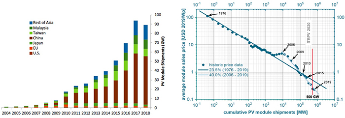
Figure 1. (Left) PV industry cumulative shipments by country from 2004 to 2018. Reproduced with permission from [2, 3]. (Right). PV learning curve showing the average module sales price as a function of cumulative PV module shipments. Several pivotal years in the history of the industry are included for reference. Reproduced with permission from [4].
Download figure:
Standard image High-resolution imageLooking forward, PV deployment will continue to grow as the global energy portfolio transitions more towards renewable energy. PV's share of total electricity supply will increase significantly because of its low cost relative to other sources. Figure 2 compares the current policy growth scenarios with the much more aggressive scenarios needed to limit global temperature rise to well below 2 °C according to the International Renewable Energy Agency (IRENA) [5] and the International Energy Agency World Energy Outlook (WEO), respectively [6]. The current policy scenario from the IRENA and WEO forecasts are labelled as the 'Planned Policy Case' and 'Stated Policies Scenario', respectively. The scenarios based on limiting global temperature rise are referred to as the 'REMap Case' (IRENA) and 'Sustainable Dev. Scenario' (WEO). The IRENA scenarios go out to the year 2050 and the WEO scenarios to 2040. Forecasts of future PV growth have increased dramatically over the last several years and now both the conservative and aggressive forecasts from the WEO and IRENA predict multiple terawatts of PV capacity will be in place within the next 20 years. While the IRENA 'REMap' scenario is somewhat more aggressive than the IEA's 'Sustainable Dev. Scenario', both anticipate approximately 5 TW of cumulative PV capacity by 2040.
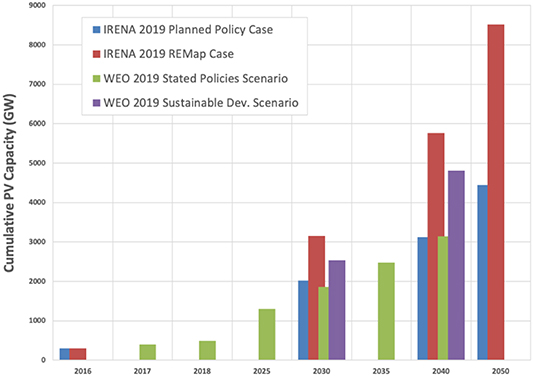
Figure 2. Cumulative PV capacity projections comparing IRENA 2019 and WEO 2019 scenarios. Note that the IRENA 'REMap' case forecasts 8.5 TW of PV capacity in 2050 and the WEO 'sustainable development scenario' case forecasts 4.8 TW in 2040.
Download figure:
Standard image High-resolution imageWhile PV is generally associated with electricity generation, many analysts and large energy companies (e.g. DNV-GL [7], Wood MacKenzie [8] and Royal Dutch Shell [9]) predict that by mid-century, PV systems will supply a large portion of the world's energy needs beyond the power sector as the result of new electricity-to-fuel technologies. Most of these technologies involve the production of renewable hydrogen from intermittent renewable electricity sources, but others involve the direct synthesis of dense energy carriers such as ammonia. Even by the end of this decade, PV systems are anticipated to be a major energy source for dense fuel production, energy intensive commodity chemicals and processed metals [10].
Given PV's critical role in the emerging global energy system, it is critical to assess the state of the photovoltaics field and the technology challenges that must be addressed to maximize future impact. This roadmap outlines critical areas of research and development involving the most promising PV conversion technologies. These include crystalline silicon and cadmium telluride that are produced at industrial scales today, as well as several promising technologies that may reach commercial production in the future. As PV continues to mature, the technical challenges become greater, requiring more rather than less effort to continue progress.
The roadmap also examines important topics that cut across all PV conversion technologies. For continued PV growth, large financial investment and hence bankability are required; these depend on PV system energy yield forecasts, service life and system degradation predictions, and improving stability through research and development. Similarly, next generation characterization techniques are critical for all PV researchers to develop new technology and reduce costs. Advancement of multiple energy storage technologies can increase long-term PV market penetration and dispatchability. Research and development of novel substrates and cell architectures can enable and foster rapid growth in new markets such as building integrated photovoltaics, aviation, defence applications, and beyond.
This roadmap is intended to provide the reader with an overview of a rapidly evolving field at a time when carbon emission reductions and the global energy transition are increasingly important topics. To aid readability, certain subjects such as balance of system components and transparent conducting oxides are not included, and the size of each section is limited. However, references are included to provide further reading where desired. This roadmap was produced by PV technology and industry experts across the world, and we hope it will serve as a valuable reference for both seasoned enthusiasts learning about different specialties or those just discovering the amazing potential of photovoltaics.
Acknowledgments
G W would like to thank Paula Mints of SPV Market Research for providing 2019 cumulative global installed PV capacity and global PV module manufacturing capacity data.
2. Trends in crystalline silicon photovoltaics
Stefan W Glunz1,2 and Pierre Verlinden3,4
1 Fraunhofer Institute for Solar Energy Systems ISE
2 University of Freiburg
3 Amrock Pty Ltd
4 University of New South Wales
2.1. Status
The exponential growth of photovoltaics from small manufacturers to today's fully automated 150 GW industry was mainly driven by crystalline silicon solar cells. The rapid development of silicon photovoltaics in terms of efficiency improvement and production cost reduction enabled a strong reduction of module prices (see figure 1 in section 1 - Introduction). In the following we will try to give an overview of important aspects and trends not only looking at technological improvements but also at some of the significant changes in mass production environment.
Evolution of industrial cell architecture—Silicon solar cells with diffused pn junctions were invented already in the 1950 s shortly after the first semiconductor diodes [11]. In the beginning boron diffusion into arsenic doped wafers was used to create the pn junction, however, phosphorus diffusion into boron-doped wafers is the standard industrial technology of today. After switching from n-type to p-type wafers in the 1960 s, the introduction of the aluminium back surface field (Al-BSF) [12] by alloying the rear contact into the base resulting in n+pp+ structure allowed for a reduced recombination at the rear side. This rather simple structure with screen-printed contacts (see figure 3(a)) has maintained a leading position with 70%–90% market share over many of the last decades. The source of its success was a stable device, a robust process sequence and a constant increase of efficiency that is mainly due to evolutionary changes such as improved metal pastes that increase the quality of the Al-BSF by reducing the recombination parameter Jo of the pp+ rear high-low junction, or that allow contacting front emitter profiles with lower surface doping.

Figure 3. Silicon solar cell structures: (a) Al-BSF, (b) PERC.
Download figure:
Standard image High-resolution imageHowever, around 2013 the efficiency of industrial Al-BSF cell plateaued around 20%. This made it attractive to substitute the fully contacted Al-BSF cell by the Passivated Emitter and Rear Cell (PERC) cell structure with local rear contacts (see figure 3(b)), resulting in better electrical and optical properties. The potential of this cell structure was already proven in 1980 s [13] but was limited to laboratory processes due to the high cost compared to the efficiency gain. The transfer of the PERC technology to industrial mass production theoretically had a relatively low threshold for the industry since only two process steps had to be added to the Al-BSF process flow, i.e. the rear surface passivation layer and the fine patterning of the local rear contacts. However, it took several decades to finalise a cost-effective PERC process. Several factors have contributed to the introduction of the PERC in low-cost large-volume fabrication and to the efficiency improvement to values between 22% and 23.4% in production:
- Introduction of the rear surface passivation with aluminium oxide by Plasma Enhanced Chemical Vapour Deposition (PECVD) and formation of a local Back Surface Field (BSF) by laser ablation of the rear passivation layer and Al alloying.
- Introduction of a selective emitter process in low-cost manufacturing, either through an 'etch-back' process or laser-doping process.
- Reduction of the width of the front metallization fingers, from about 100 μm to less than 30 μm in large volume production, while, at the same time, reducing the contact resistance for lightly phosphorus-doped silicon.
- Addition of a low-cost hydrogenation step at the end of the cell process for the passivation of bulk defects and deactivation of the boron-oxygen complexes responsible for the Light-induced degradation (LID).
- Re-emergence of mono-crystalline silicon wafers as a consequence of cost reduction in Czochralski silicon ingot fabrication as well as the introduction of diamond wire sawing.
- Cleaner production environment and better contamination control throughout the entire process from silicon feedstock to modules.
And at the module level:
- Design of PV modules with half-cells, allowing to reduce by a factor of 4 the loss due to the series-resistance of cell interconnection, improving the power output at Standard Testing Conditions (STC) by about 1.5%.
- Increasing the number of busbars from 2 to 5, while maintaining the same shading factor, and finally switching to multi-busbars using round wires (9 to 15 wires) instead of flat ribbons as interconnections.
In parallel with the PERC cell, other high-efficiency cell structures were transferred to mass production, such as the interdigitated back contact (IBC) solar cell [14] or hetero-junction solar cells (SHJ) [15] (see figure 4 and next section). Despite their high efficiency potential, their market share is still limited. This is probably due to the standardization of technology in mass production as described in the following section. However, since the market demands a continuous increase in module efficiency, these and other technologies might play an important role in the future.

Figure 4. Silicon solar cell structures: (a) i-TOPCon, (b) heterojunction (SHJ) in rear junction configuration, (c) back contact cell (IBC) with heterojunction contacts.
Download figure:
Standard image High-resolution imageDevelopment of production technology—During the period 2010 to 2020, the silicon PV industry went through a period of significant changes, including a rapid decrease in manufacturing cost (more than −15% per year in average) and a continued increased in efficiency (+2% relative per year) and module power (typically +5 W per year at the beginning of the decade, increasing much faster nowadays due to larger wafer sizes). The manufacturing cost reduction was driven by an increased collaboration between manufacturing partners, or even competitors, which accelerated the learning curve (see figure 3 in the general introduction). This resulted in a standardization of the technology, including standardization of cell (and module) design or process, and a complete alignment of the supply chain (equipment, materials, chemicals). The learning rate increased in absolute from a 40-year historical value of −20% decrease in cost for every doubling of the cumulative production to about −30% in the last decade) [16].
The latest comers in silicon PV manufacturing benefit from cheaper production tools with higher productivity, for example:
- More automation: increased labour productivity from 10 Direct Labour (DL, i.e. full time equivalent operator) per annual production of 1 MW (in 2010) to less than 1 DL MW−1 in 2020.
- Larger cells: from 125 mm square wafers in 2010 to 166 mm in 2020, or even 210 mm.
- Thinner wafers and less kerf-loss in slicing: the diameter of wires for slicing silicon wafers went from about 150 μm to less than 50 μm during the last decade.
- More wafers per batch in diffusion furnaces: from about 500 wafers per batch to 1600 wafers per batch in 2020.
- Higher throughput: from 1800 to 8000 wafers per hour with some tools in 2020.
2.2. Current and future challenges
What's next?—The silicon PV industry has embraced a continuous effort in efficiency improvement and increasing module power (from 250 W to 500 W in the last decade), which resulted in the decrease of the relative contribution of the module cost to the total PV system cost where the land and installation costs are becoming more important). One of the key challenges is to continue making such improvements described in the Status section. As manufacturers are in an extremely competitive environment, a challenge is to make high stake decisions on the best technology paths forward. Generally speaking, the roadmap for silicon solar cell development calls for the introduction of passivating contacts to the mainstream high-volume production of PV devices, then a possible switch to n-type material and finally the introduction of tandem cells. Below we describe challenges for the different technology classes.
PERC cell—The PERC cell being the actual 'workhorse' of the PV industry, the key challenge is to maintain its major role by continuous performance improvement and cost reduction. In terms of cost reduction, the production of PERC cells has the advantage that the entire supply chain is aligned and standardised to this technology. Increasing the throughput of the tools and automation are the main avenue toward lower cost of manufacturing. One of the most recent approaches is to increase the wafer size up to 210 mm which poses enormous challenges not only in cell manufacturing but also in module design and assembly, and potentially module reliability. In terms of efficiency improvement, the task is starting to be very difficult, as the efficiency in production has reached 23.3% and the practical efficiency limit of this structure is about 24.5%. Several key challenges should be mentioned:
- to obtain and maintain a high ratio of minority carrier lifetime (in μsec) and the wafer resistivity (in Ω cm), greater than 1000 μsec Ω cm−1. For example, the best silicon wafer manufacturers are now able to maintain a carrier lifetime to resistivity ratio greater than 2000 (μsec Ω cm−1) in production for n-type wafers;
- to continuously reduce the metal coverage fraction, by reducing the finger width to less than 30 μm and removing the busbars (measuring and sorting busbar-less cells is a major challenge);
- to improve the rear contacts of PERC cells by reducing the percentage of voids created by the dissolution of silicon into the aluminium layer;
- to improve the contact resistance for lightly doped phosphorus emitters;
- to develop other materials (other than SiNx and Al2O3) for the surface passivation layer;
- to introduce some of the passivating contact technologies originally developed for SHJ or tunnel oxide passivating contact (TOPCon) (see below);
- to improve the bifaciality (ratio between the rear and front efficiency) without impacting front side efficiency.
Bifacial modules—Although they have been commercially introduced more than three decades ago but did not receive the expected consideration because of cost, bifacial PV modules have done a remarkable come-back since 2018. Bifacial modules are now considered as one of the standard technologies for ground-mounted applications, with a fixed tilt structure, on a tracker or even in a vertical North-South orientation. By reducing the metal coverage on the rear side, n-type PERT (Passivated Emitter Rear Totally diffused) or TOPCon solar cells can reach 80%–95% bifaciality, while PERC solar cells made on p-type substrates have typically a 65%–75% bifaciality, lower than for n-type because of greater metal coverage to form the local Al-BSF and shorter effective carrier lifetime. The additional annual energy provided by the bifacial modules is highly dependent on the reflectivity of the ground creating the albedo, a measure of the diffuse reflection of solar radiation, and bifaciality. It varies from a few percent's, typically 6% for PERC and 9% for TOPCon or SHJ cells, up to about 25% in the best cases (ground with very high reflectivity, like snow or white gravel). The overall system design plays an important role to provide a benefit in energy yield (height from the ground, array-to-ground area or coverage fraction, rack design, module orientation, tracking or not). It is particularly important to avoid any shading of the backside of the modules [17]. Research in modelling the energy yield of bifacial PV modules is still ongoing, as well as research to increase the bifaciality of PERC solar cells.
Silicon heterojunction solar cells (SHJ)—Heterojunction solar cells also known as HIT [15] cells make use of passivating contacts based on a layer stack of intrinsic and doped amorphous silicon (see figure 4(b), SHJ in rear junction configuration). Due to their superior surface passivation quality, SHJ cells hold the record for open-circuit voltage at one sun of 750 mV. In recent years, the fill factor was strongly improved due to a better understanding of carrier transport and interface carrier recombination [18]. The main challenge of amorphous silicon passivating contacts is the parasitic absorption in the front layer stack resulting in a somewhat lower short-circuit current compared to cells with a diffused emitter. This can be overcome by using IBC cell structures (see below) or using SHJ structures as the bottom cell in silicon-based tandem cells where parasitic absorption of blue light is no issue.
One of the biggest technological challenges of this promising cell structure is that no processes with temperatures above 200 °C can be used after the deposition of the amorphous silicon layer. This excludes the well-established fired screen-printed metal contacts and thus requires alternatives routes using low-temperature pastes or plated contacts. Strong activities to establish fabrication lines with high throughput able to compete with the current standard production lines are currently under way. For SHJ technology to become mainstream, it will need to overcome the challenges of the higher cost of tools for cell production, the reduction of the silver usage or replacement by copper by developing Cu-plating technology, and the reduction of indium usage in the transparent conductive oxide (TCO) layer.
Polysilicon-based passivating contacts (TOPCon)—the TOPCon structure is an alternative to SHJ for passivating contacts, but it is a much newer technology in industrial production. It consists in adding a thin tunnelling silicon dioxide (about 1.5 nm) and a doped polysilicon layer between the silicon substrate and the rear metal contact. In the case of an n-type substrate, a phosphorus-doped polysilicon layer is used as the rear contact structure. Efficiencies of 25.8% (dedicated area, in laboratory) [19] and 24.6% (total area, in the industry) [20] have been demonstrated with this structure and n-type substrates. The TOPCon technology is fundamentally compatible with the conventional silicon solar cell process. It just adds two to four steps in the normal cell process. It does not have the advantage of 30 years of production history like SHJ but might be easier to integrate with existing production lines. Currently, the main current challenge is to adopt a well-accepted standard process sequence for the industry that would enable a cost-reduction roadmap.
Interdigitated back contact (IBC) solar cell—Solar cells with interdigitated back contacts (IBC) were always regarded as the cell architecture with the highest efficiency potential by avoiding shading losses [21]. The company SunPower is the pioneer of developing a mass-production IBC cell [14]. Indeed the first industrial solar cell with efficiencies clearly above 20% was based on this concept. The biggest challenge for this cell structure compared to a conventional cell structure is the higher process complexity, with doping and contacts of both polarities on one side, requiring a relatively fine patterning of at least three levels with a precise alignment between them. Therefore, to be cost-competitive, it is a major requirement that its efficiency should be significantly higher than the one of PERC-type cells. SunPower has reached a major boost in efficiency above 25% by applying passivating contacts. The current efficiency record for silicon solar cell of 26.7% [22] combines an IBC structure with heterojunction passivating contacts (see figure 4(c)). IBC cells with polysilicon-based passivating contacts have also reached excellent efficiencies (26.1%) [23]. Recently, new rear patterning process approaches, e.g. using tunnel structures, have been presented which might help to reduce process complexity [24].
n-type vs. p-type—While the first efficient silicon solar cell was made on a n-type substrate, the selection of p-type as the substrate of choice comes from the observation that a boron-doped p-type substrate was less susceptible to carrier lifetime degradation after electron irradiation, a major requirement for solar cells for space power applications. Many years later, aluminium diffusion was used to form a BSF at the same time as forming a positive electrode. When the Al-BSF process is not used, the n-type substrate might become the substrate of choice due to its minority carrier lifetime being higher and less sensitive to donor-like metallic impurities, like iron. In general, for solar cell structures using passivating contacts instead of Al-diffusion, like for SHJ or TOPCon, n-type substrates are preferred.
Multicrystalline vs. Monocrystalline—For many years multicrystalline Si held a dominant market share because of lower costs, mostly due to less energy consumption and higher throughput per crystallization tool. With increasing quality of the cell structures (surface passivation etc.), material quality plays a more important role than in the past. For example, it resulted that, when upgrading from a conventional Al-BSF structure to a PERC structure, for the same additional cost, the power gain was greater with monocrystalline wafers than with multicrystalline wafers. In addition, the slicing cost of monocrystalline wafers is significantly lower for mono- than for multicrystalline wafers (higher slicing speed, less kerf loss and more wafers per kg of silicon). Currently very interesting technological options to close the efficiency gap between mono- and multicrystalline are being investigated, such as the growth of cast monocrystalline material using a seed crystal to achieve better crystallographic quality (also known as quasi-mono). Excellent efficiencies have been achieved using cast monocrystalline material which shows that research on improved crystallisation processes opens new horizons for cast silicon.
Stability and Energy Yield—As efficiency increases, an obvious benefit is the improvement of the temperature coefficient of efficiency, but increasing energy yield and product lifetime are other paths for improvement. Thus, the already proven long-term stability of crystalline silicon modules of 25–30 years should be extended to 40 years. This can be reached by improved module technology e.g. using glass-glass modules or new encapsulation materials. Use of bifacial modules will additionally increase the energy yield. A more accurate prediction of module performance and energy yield is an urgent task with increasing fraction of PV in the energy market.
Scaling and Sustainability: In a 100% renewable energy economy, PV will play a major role. A key challenge is to increase the annual production of PV modules to 3–4 terawatts annually by 2040. Materials sustainability in the fabrication and recycling of PV modules will become a significant issue including the reduction of CO2 emissions in silicon material, cell and module production. Again, increasing the efficiency is of key importance since it reduces the necessary amount of energy-intensive materials such as crystalline silicon and module glass, i.e. it reduces the energy payback time [25]. Also a direct reduction of energy use i.e. CO2 emission by using alternative silicon material processes such as epitaxial wafer growth [26] should be considered. Moreover, rare or costly materials, such as silver for the metal contacts or indium for TCO layers in SHJ cells, should be reduced or even avoided.
2.3. Advances in science and technology to meet challenges
Understanding material properties and degradation effects—Although silicon is the best understood semiconductor, there is still research needed to refine the characterisation of its basic properties and defects. Due to the indirect nature of the bandgap structure of silicon, Auger recombination rather than radiative recombination limits its theoretical efficiency [27]. The strongly improved surface passivation developed in the last decade enabled determining the Auger-coefficients more accurately.
Additionally, a detailed analysis of defect recombination in silicon is of major importance. While many of the 'classical' impurity-based point defects as Fe are well understood, metastable defects causing LID [28] or Light and elevated Temperature Induced Degradation (LeTID) still need further investigation. With improved quality of the cell structures, i.e. surface passivation, such effects are getting more important. Especially the contradictory role of hydrogen in silicon is a very interesting field of research. While hydrogen is beneficial for the regeneration i.e. deactivation of LID, it seems to play a negative role for the extent of LeTID [29]. Thus, a deeper understanding of the underlying processes will help to reduce the degradation effects which cause losses and uncertainty in field application.
Surface passivation and passivating contacts—All record silicon solar cells with total-area efficiencies above 24.5% have one feature in common: passivating contacts to reduce carrier recombination. Technologies based on poly-crystalline silicon (TOPCon [30]) or amorphous silicon (SHJ [18]) have proven to yield excellent surface passivation and good carrier transport properties. However, the challenge is the parasitic absorption of light resulting in lower currents especially when applying such passivating contacts to the front side. Therefore, either developing an elegant patterning technology resulting in selective passivation contacts (similar to diffused selective emitters) or using transparent materials such as metal oxides are interesting routes to achieve solar cells with perfect electrical and optical properties.
Silicon-based tandem cells—Single-junction crystalline silicon solar cells have a theoretical efficiency limit of between 29.4 and 29.5% [27, 31]. The silicon PV industry has enough options to drive the efficiency of single junction silicon solar cells to a practical technical limit of about 27.5% in laboratory and 26% in production. Due to the high development speed, this point might be reached in the next decade. Further efficiency improvement is only possible with new multi-junction cell structures. Silicon-based tandem solar cells offer one of the most promising solutions for efficiencies above 28% (see chapter 'Tandem Solar Cells'). A monolithic combination of silicon as the bottom cell with III–V based top cells has already demonstrated in laboratories efficiencies well above 30% and thus above the theoretical limit of a single junction silicon cell. The biggest challenges for this route are the development of a defect-free direct growth of the III–V top cells on the unpolished surface of a low-cost silicon cell and a strong cost reduction in the fabrication of the III–V layers. A potentially cheaper route is the use of perovskites as top cells with current record efficiencies above 28%. In this case, long-term stability and low-cost mass production have still to be shown.
2.4. Concluding remarks
Cost reduction and efficiency improvement in silicon PV technology can be continued by addressing the different challenges outlined in this roadmap. Building on a largely standardized industry and a steep learning curve, crystalline silicon-based PV is well positioned to meet the challenge of producing many terawatts of power. Research in passivating contacts provides a common route for silicon PV technologies to improve. Improved module technology, as well as careful defect analysis and control, are key paths to increase reliability. Ultimately, tandem technologies can increase performance beyond the single junction theoretical limit, however significant research is still required to enable this at low costs for the mass market. Despite the maturity of this technology, continuing research and development have become more critical than ever to navigate and develop the diverse possibilities.
Acknowledgments
S G and P V would like to thank sincerely all colleagues in the field of silicon photovoltaics whose enthusiasm and hard work have helped the progress of this technology.
3. CdTe
Wyatt K Metzger1 and Gang Xiong2
1 National Renewable Energy Laboratory
2 First Solar Inc.
3.1. Status
CdTe solar cell technology has reached an unsubsidized levelized cost of electricity competitive with wind technology, slightly less than Si PV, and generally less than all other electricity generation sources. Typically, the module manufacturing is an inline process, where glass enters a factory and exits as a completed solar panel in several hours. The semiconductor layers are several microns thick, and they cost just a few pennies per watt to manufacture. Capital and energy expenditures are relatively low. In 2019, cumulative CdTe module shipments reached 25 GW.
CdTe solar technology has evolved significantly over time. Certified cell efficiencies reached 10% in the 1980s [32], and in the 1990s, efficiency exceeded 15% using a glass/SnO2/CdS/CdTe structure and an anneal in a CdCl2 ambient followed by Cu diffusion [33]. In the 2000s, cell efficiency reached 16.7% using sputtered Cd2SnO4 and Zn2SnO4 for the transparent conducting oxide (TCO) layers [34]. In the past decade, First Solar and General Electric exchanged new world-record cell efficiencies, which climbed to 22.1% [32]. Costs have steadily declined, and CdTe solar technology is bankable and scalable. First Solar is forecasting 7.6 GW of annual capacity by the end of 2020, and modules are being installed across the world for multiple applications. Although most installations have been for utility-scale power plants, CdTe technology increasingly has been adopted in roof-top systems and building-integrated photovoltaics (figure 5).
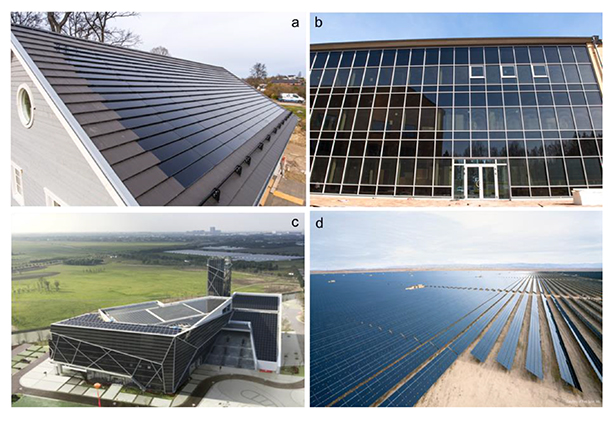
Figure 5. (a) Residence with CdTe PV tile in Europe; (b) office building with semi-transparent CdTe panels in Europe; (c) exhibition hall with 5556 m2 of standard, semi-transparent, and artistic CdTe panels in Asia; (d) Topaz solar plant owned by BHE renewables in the United States. Reproduced with permission from (a)–(c) Advanced Solar Power, (d) First Solar Inc.
Download figure:
Standard image High-resolution imageFigure 6 shows a typical CdTe solar cell schematic. The recent performance gains have come in part by nearly maximizing photocurrent through optimizing the cell optical properties, removing parasitically absorbing CdS, and introducing lower-bandgap CdSexTe1-x. The CdSexTe1-x grades the absorber bandgap from ∼1.4 to 1.5 eV and increases the carrier lifetime, thereby increasing photocurrent collection without a commensurate loss in photovoltage. The adoption of ZnTe in the back contact also significantly improves contact ohmicity, thereby improving performance.
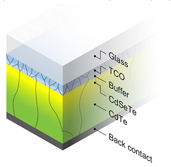
Figure 6. Schematic from [36] of a CdTe solar cell. The TCO layers are typically a few hundred nanometers thick. The buffer may consist of tens of nanometers of CdS, MgZnO, or another material. The back contact generally has a layer such as Te or ZnTe followed by metallization.
Download figure:
Standard image High-resolution image3.2. Current and future challenges
Efficiency. A near-term focus is to increase cell efficiency to 25%. Photocurrent and fill factor have nearly been maximized for current technology. Consequently, the greatest challenge is to increase photovoltage by overcoming fundamental material issues such as recombination and low carrier concentration. GaAs solar cells have achieved open-circuit voltage (Voc) greater than 1.1 V with a bandgap of 1.4 eV, whereas production CdTe solar cells with a similar bandgap have been limited to a Voc of 800–900 mV [35]. Once Voc is increased, further gains in fill factor are possible.
Carrier Concentration. Like many polycrystalline thin-film technologies, controlling absorber carrier concentration has been difficult. The rapid deposition of the absorber layer on nanocrystalline substrates leads to micron-size grains and extremely poor carrier lifetime. Consequently, CdTe technology has relied on a CdCl2 anneal that passivates the grain boundaries, interfaces, and bulk, thereby increasing performance. Afterwards, Cu is traditionally diffused into the CdTe to achieve a low-resistance back contact, increase CdTe hole density, and optimize efficiency. However, the Cu and Cl form a compensated defect chemistry. After decades of adjusting these processes, the useful hole density has consistently been limited to the order of 1014 cm−3. This has contributed to limiting production cell Voc to 800–900 mV.
Group-V Dopants. Recent efforts in doping single-crystal CdTe with Group-V elements (e.g. P, As, Sb) demonstrated that CdTe is capable of 1016–1017 cm−3 hole density with radiatively limited lifetimes and Voc exceeding 1 V for the first time [35]. Group-V doping of polycrystalline CdTe has now resulted in elevated hole density of 1016–1017 cm−3, comparable to that in single-crystal material [36]. The Group-V dopants are far more stable than Cu under heat treatment or light/electric bias. This has increased energy yield and provides a platform to increase efficiency toward 25%.
Front (p-n junction) Interface. The Voc of Group-V doped CdTe devices is less than expected from absorber hole density and lifetime measurements. This can be reconciled by front interface recombination consistent with Voc(T) data, other experimental observations, and computational modelling [36]. Simultaneously optimizing the p-n junction interface and carrier activation remains a challenge to increase performance.
Enhanced Energy Yield. CdTe solar technology using Cu has achieved state-of-the-art long-term degradation less than 0.5% yr−1 as well as excellent field performance. However, there is room to improve. Cu migration has been a primary limiting factor of cell stability. Early results with Group-V doping and no Cu show far superior cell stability and energy yield compared to their Cu counterpart, thus providing a path to increase energy yield and product lifetime beyond today's technologies.
Carrier Lifetime. CdSeTe has increased carrier lifetime toward tens of nanoseconds. But a further tenfold increase is possible, which would enhance performance and enable new paths to improve efficiency.
Back-Contact Passivation, Reflectors, and Fields. As more minority carriers reach the rear contact, back-surface passivation and electron reflectors can boost performance toward 28% efficiency according to modelling or comparisons with GaAs [37]. Today, back-surface recombination velocity is about 105–106 cm s−1, so back-surface passivation methods are needed.
Transparent Back Contact for Bifacial and Tandem Cells. Bifacial and tandem solar cells are both considered future directions in research and development. A transparent back contact is a prerequisite for each application. Coupling a transparent back contact with improved back-surface passivation and long absorber lifetimes can establish effective bifacial CdTe solar technology.
Critical Mass. Today, only a handful of non-industry groups are making polycrystalline CdTe solar cells worldwide. CdTe PV provides a combination of real-world impact and rich research needs. Although concerns exist about toxicity and abundance, the CdTe film is very thin and is generally non-reactive, encapsulated, and recycled. The greatest sources of ingested Cd are from food and coal emissions, and Te supply is primarily a byproduct of Cu mining. Several studies have indicated that CdTe PV manufacturing has the lowest environmental footprint compared to other technologies [38]. Fthenakis et al estimated that Te reserves are sufficient to support as much as 10 TW cumulative this century [39]. At end of life, approximately 95% of the semiconductor materials are recycled for use in new modules.
3.3. Advances in science and technology to meet challenges
Synthesis, characterization, and theory need to be advanced well beyond the state of the art to meet the challenges outlined above.
The best dopants and activation methods are still not clear. Activation is defined as the ratio of the hole density (carriers cm−3) relative to the dopant density (e.g. P atoms cm−3). For Group-V defect chemistry, 0.3%–3% activation is typical. As a result, high doping incorporation levels (1018 cm−3) induce intra-grain potential fluctuations, which can reduce Voc by 100 mV [36]. Methods have been developed to image Group-V elements on Te lattice sites, but advances are needed to understand how unactivated dopants reside in the lattice. Theory and experiment need to describe the interaction of dopants with impurities such as Cl, and novel synthesis methods to increase activation are critical.
Understanding the science of the p-n junction interface and carefully manipulating its properties is another frontier. Methods need to be developed to measure the band alignment and electron density in this buried interface after device fabrication to engineer less recombination. In addition, high-throughput measurements of interface recombination velocity with improved sensitivity are needed to gauge and accelerate experimental efforts. Recent work has enabled atomically smooth planar cleaves of the junction interface in an inert (O2-free) high purity ambient to examine previously unreported interfacial chemistry [40]. Identifying interface defect chemistry and its correlation with electronic states is desired to guide interface engineering to reduce recombination and improve performance. Significant research is required to achieve chemical passivation and field manipulation at the buried junction interface in conjunction with new processes to increase dopant activation.
Advances in new materials, nanolayers, two-dimensional structures, and/or bilayer designs can extract carriers while passivating the front and back contacts. Recent studies with Al2O3 and other materials have demonstrated significantly reduced interfacial recombination velocity [41], but these materials are not suitable for low-resistance contacts. In addition, sophisticated materials research is needed to develop transparent back contacts to allow light to pass through a CdTe top cell in tandem PV devices or to enable bifacial CdTe PV.
There are a number of next-generation technology possibilities. These include but are not limited to seeding large grain growth with low-cost methods, achieving nucleation that removes the need for the CdCl2 anneal, establishing n-type absorbers, creating new cell architectures such as homojunctions, and implementing interdigitated back contacts.
3.4. Concluding remarks
CdTe photovoltaic technology has reached large-scale production and levelized cost of electricity competitive with conventional electricity generation sources, yet a tremendous amount of foundational research and development still remains to enable this technology to reach its full potential.
4. CIGS
Lorelle M Mansfield1 and Billy J Stanbery2
1 National Renewable Energy Laboratory
2 HelioSourceTech LLC
4.1. Status
The group I-III-VI chalcopyrite (Ag,Cu)(In,Ga)(S,Se)2 semiconductor alloys, commonly known as CIGS, are particularly suitable absorber materials for solar cells. Their direct bandgaps range from ∼1 to 2.6 eV, they have high absorption coefficients and favourable intrinsic defect properties that enable high minority carrier lifetimes, and solar cells therefrom are intrinsically stable in operation. Their first reported efficiency was a 12% single-crystal device in the mid 1970 s [42]. Subsequently, CIGS thin-film absorbers, processing, and contacts have improved dramatically, yielding 23.4% small-area thin-film cells [43]. Current record module efficiencies are 17.6% on glass (0.72 m2 total area), and 18.6% on flexible steel (1.08 m2 aperture area).
The history of CIGS cell technology efficiency improvement is summarized in figure 7. Briefly these stages can be characterized as (1) evaporation of the compound CIS; (2) reactive elemental codeposition of bilayers; (3) selenization of sputtered metal precursors; (4) chemical bath deposition of CdS with ZnO:Al as the emitter; (5) gallium alloying; (6) sodium alkali incorporation; (7) three-stage codeposition; (8) alkali heavy-ion-exchange post-deposition treatment; and (9) sulfurization-after-selenization (SAS). Progress has not been linear [42], and the full potential of optimizing the complex interactions of these techniques, as well as others in development (e.g.: silver alloying [44]), has not yet been realized. Many researchers specializing in CIGS believe that 25% efficiency will be achieved.

Figure 7. Annotated history of record CIGS cell efficiencies and key innovations [42].
Download figure:
Standard image High-resolution imageCIGS is a versatile material that can be fabricated by multiple processes and implemented in different form factors. Currently, four main categories of deposition techniques are employed when fabricating CIGS films: (1) metal precursor deposition followed by sulfo-selenization; (2) reactive codeposition; (3) electrodeposition; and (4) solution processing. All recent world records and the most commercially successful have utilized two-step sulfo-selenization of metal precursors or reactive codeposition [45]. CIGS can also be deposited on a variety of substrates including glass, metal foils, and polymers. Glass is suitable for making rigid modules, whereas metal and polymer foils allow for applications that require lighter-weight or flexible modules. As global energy markets evolve to value greenhouse gas emission mitigation and circular economy considerations, the relatively benign environmental impacts of CIGS (particularly without CdS) compared to other PV technologies become another competitive asset [46]. With further advances, CIGS can fulfil the promise of versatile, low-cost solar cells, and provide a foundation for high-performance low-cost multijunction tandem modules [47] (see section 7).
4.2. Current and future challenges
CIGS commercial production is currently 1 GW. It has been limited primarily due to the challenges of cost-effectively scaling both module size and production volume using SAS and co-evaporation processes that produce high module efficiencies. The efficiency gap between record small-area cells and commercial modules is greater than that of more mature technologies currently in large-scale production, predominately because of the challenges of achieving large-area device uniformity. Monolithic integration of multiple cells in series by patterning films deposited on a single substrate is a method available when depositing on insulating substrates or insulated metal substrates. This reduces integration costs compared to discrete device technologies like silicon (or thin film cells singulated from conducting substrates), but Kirchhoff's current law then demands superior uniformity since cells cannot be selectively matched. A key challenge is to solve these problems by improving production tool designs and in situ control metrologies.
Optimizing CIGS modules for lower levelized-cost-of-electricity (LCOE) requires balancing the complex interplay of manufacturing cost, efficiency, energy yield, and durability. One conceptual benefit of thin-film PV is lower direct semiconductor materials cost than wafer-based PV. Realizing lower costs in production requires high input-materials utilization and low raw-materials conversion costs. Unlike silicon PV, where cells can be fabricated in one location and modules in another, monolithic integration necessitates colocation of the manufacturing value chain. This makes large-scale thin-film module production facilities both more capital intensive and more cost efficient when utilizing rapid processing technologies. Solving the challenges of accelerating diffusion-limited SAS processes and increasing the materials utilization of high-rate codeposition tools are essential. The challenge of cost-effective cadmium-free buffer deposition at scale is also significant. The glass-glass architecture of most modern fielded CIGS modules provides durability [49] and energy yield [47] comparable to silicon. As customers demand increasingly lower energy-yield degradation rates, another key challenge is to establish whether process, device structure, or module packaging modifications will be required to sequester mobile alkalis that are essential to competitive CIGS efficiency.
4.3. Advances in science and technology to meet challenges
The greatest challenge to increasing CIGS device efficiency is reducing its voltage deficit (VOC,def ) towards the AM 1.5 G detailed balance limit of solar cell parameters. VOC,def = VOC,DBL − VOC where VOC,DBL is the detailed balance limit open-circuit voltage which is a function of the bandgap of the cell [49]. For example, the record CIGS cell [43] with a bandgap of 1.08 eV (VOC,DBL = 0.827 V [49]) and VOC of 0.734 V has a VOC,def = 0.093 V. Reducing VOC,def requires reducing non-radiative recombination rates while increasing radiative recombination emission reabsorption and quasi-Fermi level splitting (QFLS). Recent progress in alkali post-deposition treatment [50] and silver alloying have reduced both grain-boundary recombination and sub-bandgap defects states that cause potential fluctuations (thus reducing QFLS), but further co-optimization is needed. Optimizing processes to increase intergrain homogeneity is a promising strategy. World-record devices that utilize sulfur substitution on the absorber Group VI lattice site showed reduced voltage deficit with Zn(O,S,OH) relative to CdS buffers, attributed to reduced space-charge region recombination [43]. Complete understanding of issues, including secondary phases, doping, and bandgap alignment, that are deleterious to the buffer/CIGS interface would provide opportunities to better match these layers based on their processing and resulting properties.
Most commercial products experience an increase in open-circuit voltage due to light-soaking (metastability), creating difficulty in accurately and inexpensively testing products, which is necessary for labelling and system sizing. Device designs that eliminate metastability or methodologies to predict and quickly measure metastability would reduce costs associated with that uncertainty. Reducing recombination at the CIGS/MoSe2/Mo contact by utilizing passivated back contacts may both enable thinner absorbers and permit reduced bandgap gradients within the absorber, increasing QFLS while reducing cost [51]. Back contact structures can also be designed to incorporate light management features increasing radiative recombination emission reabsorption [51]. Advances in processing technologies to flexibly incorporate Group I silver alloying, only implemented successfully using codeposition, and Group VI alloying, only using SAS, may also be fruitful.
Adapting laboratory processes that are optimized at low rates to high-throughput production is critically important. To maximize capital equipment utilization efficiency, manufacturing systems often utilize dynamic deposition processes which would benefit from better fundamental scientific understanding of reaction kinetics' relationships to materials properties and structure. Pertinent contexts include chemical bath deposition and spatial atomic-layer deposition processes for fabricating buffer layers. The development of metrology techniques applicable in situ for inline process control are immensely valuable to expeditious translation of laboratory methods to production optimization. Optical techniques for process control need further development, in lieu of laboratory methods less amenable to extended production runtimes. Examples include optical absorption for selenium pressure, white light, photoluminescence, and defect detection spectroscopies [52].
4.4. Concluding remarks
Research on solar cells and development of manufacturing technologies for modules fabricated from group I-III-VI chalcopyrite (Ag,Cu)(In,Ga)(S,Se)2 semiconductor alloys is far from over. This material class remains one of the most versatile in processing, substrate type, and device architecture. Fielded module studies have demonstrated these products provide low degradation rates for decades [48], so 50 year lifetimes are a realistic goal. With further advances in scientific understanding, 25% efficiency devices are within reach as are even higher efficiencies in tandem architectures as their lower-bandgap partner. Translating those device and process advances to manufacturing technology will dramatically reduce LCOE once sufficiently scaled in both module size and production volume. This will require adapting deposition processes for higher rates and to larger-scale equipment while developing suitable robust techniques for inline process and quality control.
Acknowledgments
Thank you to all those who work on CIGS PV technology, past and present, creating our vibrant and productive global community. Thanks to Al Hicks and Don Gwinner at NREL for creating figure 8. Funding for this section was partially provided by US Department of Energy Office of Energy Efficiency and Renewable Energy Solar Energy Technologies Office Agreement Number 34 352.
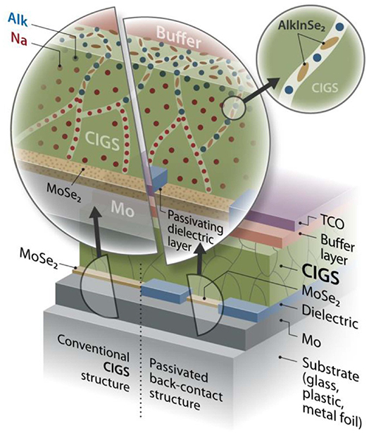
Figure 8. Cross-sectional diagram of CIGS solar cells. The conventional CIGS device structure is on the left, and an example of a passivated back-contact structure [51] is on the right. Alk refers to heavy alkalis such as K, Rb, or Cs.
Download figure:
Standard image High-resolution image5. Perovskites
Kai Zhu1, Yanfa Yan2 and Joseph J Berry1
1 National Renewable Energy Laboratory
2 University of Toledo
5.1. Status
Perovskite solar cells (PSCs) represent an emerging, revolutionary photovoltaics (PV) technology based on metal halide perovskites (MHPs)—e.g. methylammonium or formamidinium lead iodide (MAPbI3 or FAPbI3, respectively). MHPs combine several preferred characteristics for a PV absorber, such as direct bandgap with strong absorption coefficient, long carrier lifetime and diffusion length, low defect density, and easy tuning of composition and bandgap. In 2009, MHPs were first reported as a sensitizer in a dye cell configuration based on liquid hole-conducting electrolyte [53]. In 2012, the demonstration of ∼10%-efficient PSCs based on a solid-state hole conductor has triggered explosive PSC research efforts [54, 55]. Within about a decade of research, the performance of a single-junction PSC has skyrocketed to a certified 25.2%.
Figure 9 summarizes the efficiency progress for PSCs ranging from lab cells (∼0.1 to 1 cm2) to mini-modules (>10 cm2). Strikingly, most high-efficiency PSCs to date are fabricated by solution processing, which makes PSCs attractive as a potentially high-performance and low-cost PV technology. Various deposition approaches have been developed to scale up PSCs [56], leading to recent demonstration of a 802-cm2 perovskite solar module with a certified 16.1% efficiency [57]. This module performance is rapidly approaching that of established thin-film PV technologies (e.g. CdTe and CIGS). During the past few years, PSC stability has also been drastically improved via various efforts to optimize perovskite absorbers and device structures along with encapsulation strategies [58].
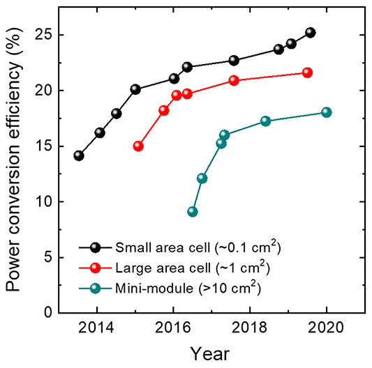
Figure 9. Significant power conversion efficiency progress for perovskite solar cells and mini-modules with different active device areas.
Download figure:
Standard image High-resolution imageAlthough there are still many unanswered technical and scientific questions to address, the high performance and scalable (printable) fabrication of PSCs coupled with low production and CapEx costs have already positioned PSCs as a potential PV technology to address terawatt-scale energy demand. Among all polycrystalline thin-film PV technologies, PSCs are uniquely capable of producing >20%-efficient devices with a bandgap near 1.7 eV or higher. These wide-bandgap PSCs can be paired with low-bandgap PSCs and other PV technologies (e.g. Si and CIGS) to form ultrahigh-efficiency tandem devices to break the thermodynamic efficiency limits of single-junction cells set by the Shockley-Queisser detailed balance theory. Thus, PSCs have multiple potential pathways to terawatt-scale energy production [59].
5.2. Current and future challenges
Stability. Achieving long-term stability under outdoor operating conditions is a major target for PSC development. At present, most stability studies are frequently conducted on small-area cells under inert environment (e.g. N2). It is critical and challenging to understand degradation mechanisms associated with various factors (e.g. light, heat, bias, moisture, O2, or their combinations). Transitioning to modules and/or tandems can introduce unique degradation pathways not available at the level of a single cell (e.g. shading, bias potential, scribing, nonuniformity, process/material compatibility). Standard packaging/encapsulation schemes need to be tailored for perovskites to ensure compatible thermal budgets and material chemistry. Furthermore, it is known that standard International Electrotechnical Commission (IEC) protocols for stability assessment developed for other PV technologies are not directly applicable to PSCs as they address known failure mechanisms based on fielded modules. At this time, such test data for assessing PSC and module operational stability is not present even if the IEC standards were relevant. Thus, it is challenging, if not impossible, to make predictions of long-term outdoor life based on standard test protocols that may not apply and for which there is not significant field data present.
Scaling Up. At present, the record performance is 25.2% for a ∼0.1 cm2 cell and 16.1% for a ∼800 cm2 module. The performance gap (∼9%) is much larger than prediction (∼3%–4%) based on the common scaling behaviour [60], which can be attributed to multiple factors including the nonuniform coating of perovskite and other device layers as well as non-ideal interconnection structure/geometry limited by material and processing constraints. The state-of-the-art PSC device stack is still under active development. Several device structures and perovskite compositions can reach a similar performance. The best scalable deposition method (solution/vapor/hybrid) can change depending on the targeted device structure and perovskite composition. Thus, it is critical to adopt a scalable fabrication process/protocol that can incorporate new improvements based on cell-level studies.
Efficiency. The single-junction PSC has reached 25.2% efficiency based primarily on FAPbI3 (bandgap ∼1.5 eV). For this perovskite absorber, a short-circuit current density near 27 mA cm−2 has been demonstrated [61]. Further advancement will likely result from increasing open-circuit voltage and fill factor via interface engineering and defect reduction. A bandgap of 1.5 eV is slightly higher than ideal for a single-junction PV absorber. Incorporating Sn into Pb-based perovskite represents a promising approach to further increase short-circuit current density [62], but Sn-induced defect and stability issues remain much more challenging than Pb-based PSCs.
Toxicity. At present, all high-efficiency PSCs contain toxic Pb, and no Pb-free PSCs have been effective. Although the amount of Pb used in PSC is small, the presence of Pb could present a challenge for PSC commercialization. This has been a subject under continuous debate since the beginning of the field. The exact impact of Pb to the environment and humans should be carefully evaluated and quantified. If Pb is indispensable for PSCs, then strategies for preventing/mitigating the potential impact must be considered [63].
5.3. Advances in science and technology to meet challenges
The PSC development is largely determined by improving material qualities by a wide range of synthetic approaches developed under the guidance of a fundamental understanding of MHP growth mechanisms [64]. Understanding the complex and interdependent perovskite formation processes (e.g. nucleation, grain growth, and microstructure evolution) has helped to tailor a wide range of highly effective growth modes (e.g. one-step growth, sequential growth, solution process, vapor process, post-deposition treatment, non-stoichiometric growth, additive-assisted growth, and structure dimension tuning). Recent efforts have shifted toward interface engineering, with a focus on reducing open-circuit voltage loss and increasing stability, especially with the incorporation of a two-dimensional perovskite surface layer. With advances on synthetic controls, the perovskite composition is on a trend to become simpler toward mainly FAPbI3. This will no doubt help to simplify the deposition approaches at scale and the basic understanding of the structure-property relationship.
Accelerated lifetime testing (ALT) based on mechanistic insight will need to play an important role in developing PSCs and modules to ensure operational lifetimes. Stability tests that differ qualitatively and quantitatively from those currently used, such as the IEC 61215 protocol, and instead target not only relevant degradation modes but also particular mechanisms of device failure are required. Science driven ALT must target specific, relevant, and, to the extent possible, universal degradation pathways. Only with the appropriate material insight will rapid experimental approaches provide predictive lifetime assessment over extended time periods. The ALT methods must be designed to address the science and associated unique behaviors of PSCs (e.g. current-voltage hysteresis and potential metastability against heat and moisture). To enable a reliable prediction of module lifetime, myriad test results across various test conditions, device architectures, and material processing approaches are necessary. Use of data-science driven approaches (e.g. machine learning or related techniques) are needed to systematically analyze complex datasets to facilitate understanding of the fundamental degradation mechanistic interdependencies and their origins.
Advanced computational methods are also needed to reliably calculate the optoelectronic, defect properties, and interfaces within the PSCs devices. These methods will enable rapid calculations to guide understanding of direct relevance to devices. The results will provide insights for addressing not only efficiency, stability and scalability, but also, toxicity issues. These will also be critical to other related issues such as recyclability and lifecycle and related environmental impacts important to a sustainable terawatt-scale technology.
5.4. Concluding remarks
Metal halide perovskites can perform as efficient single-junction thin-film solar cells, all-perovskite tandems, and are easily integrated with other established PV technologies to create hybrid tandems. Rapid advances are made in efficiency, stability, and scalability. To more rapidly progress to market, the issues outlined above must be addressed in combination to ensure the feedback between process development, scaling, efficiency, and stability. This can be done by developing ALT protocols to more rapidly assess stability, along with sophisticated computational tools and advanced data analytics. Although the net impact of Pb-based PSCs is generally positive, the potential local impact will require that technologies to mitigate toxicity issues are developed, in parallel with designing for recyclability and sustainability. The advent of PSCs has created an opportunity to develop a new efficient, scalable, stable, and sustainable PV technology that will change how energy is produced if continued efforts are made.
Acknowledgments
K Z and J J B acknowledge the support from the De-Risking Halide Perovskite Solar Cells program of the National Center for Photovoltaics, funded by the US Department of Energy, Office of Energy Efficiency and Renewable Energy, Solar Energy Technologies Office, under Contract No. DE-AC36-08GO28308. Y Y is supported by the US Department of Energy's Office of Energy Efficiency and Renewable Energy under the Solar Energy Technologies Office Award Number DE-EE0008753.
6. III-Vs: toward low cost and one-sun terrestrial operation
Aaron J Ptak1, Frank Dimroth2 and Brendan M Kayes3
1 National Renewable Energy Laboratory
2 Fraunhofer Institute for Solar Energy Systems ISE
3 Antora Energy
6.1. Status
III–V materials yield the highest photovoltaic (PV) conversion efficiencies, reaching 29.1% for single-junction GaAs at one sun illumination and 47.1% for a six-junction device under concentrated sunlight [57]. They are also thin (absorber layers typically have thicknesses between 2 and 5 µm) and can therefore be processed as light, flexible devices that can be applied on curved surfaces. III–V devices are very stable, with a track record of high performance in demanding applications like space. Consequently, these devices fulfill the requirements of current and future PV applications. This tremendous value comes at a cost, however, currently $100–200 Wp −1. This is more than two orders of magnitude higher than today's GW-scale technologies. These current high costs also represent the promise of III–Vs: they will continue to have the world-leading conversion efficiency, low mass, flexibility, and stability necessary for current and future solar applications, but they also have the opportunity to follow a familiar path of increasing scale combined with manufacturing technology advancement to enable significant cost reductions.
Current costs broadly fit into three categories: substrates for epitaxial growth, semiconductor deposition itself, and back-end processing. Each of these needs to be decreased together to produce lower device costs. GaAs and Ge substrates are approximately $100 per 6'' wafer at high volumes, already representing $20–25 Wp −1 at one-sun for the substrate alone. Final substrate costs need to be closer to $1 per 6'' wafer, which could be realized through substantial reuse of the wafer or the development of direct growth on a less expensive template, e.g. solar-grade Si, that will still lead to essentially perfect epitaxy. The dominant deposition process for III–Vs, metalorganic vapor phase epitaxy (MOVPE), is responsible for virtually every record III–V device efficiency; however, it has historically been deemed an expensive growth technique due to high precursor costs, relatively low utilization of those precursors, and batch-style growth runs that take hours to complete. Recent research has greatly increased growth rates and shown much higher utilization of the chemical precursors, both using MOVPE and hydride vapor phase epitaxy (HVPE), while HVPE also addresses precursor costs. Back-end processing today involves a large number of labor intensive, expensive, and relatively low-throughput process steps, including photolithography, manual spin coating and contact alignment, and metal evaporation and liftoff.
III–Vs will be able to access much larger markets when these costs are reduced. This is especially true for area-constrained applications that value the high efficiency that III–Vs deliver. Because of the differentiating high efficiency of III–Vs, there are some intermediate markets where this technology will compete without having to achieve the same or lower costs than incumbent, mainstream PV technologies, including military applications, high-altitude long-endurance (HALE) vehicles, large space constellations in low-earth orbit, thermophotovoltaics, and solar-supported electric cars and planes, as shown in figure 10. This affords an opportunity for technology development and staged scale-up to ensure continuous cost reduction through increasing production volumes.
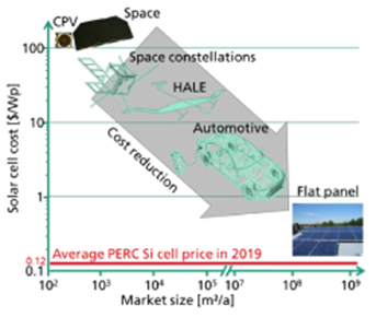
Figure 10. Cost reduction of III–V solar cells will open new markets with significantly larger volume. Space and concentrating photovoltaics are already existing markets for III–V multi-junction solar cells, space constellations and HALE vehicles as well as automotive integration are under development. Reproduced with permission from (http://pvinsights.com) (17.1.2020). Graph © Fraunhofer ISE after H Helmers.
Download figure:
Standard image High-resolution image6.2. Current and future challenges
Fortunately, III–V solar cell devices themselves do not need substantial improvement in technology because they already boast the highest conversion efficiencies available. The current record for a single-junction GaAs cell is 29.1% [57], which is closer to its Shockley-Queisser limit (33.5%) than any other PV technology. III–Vs have also proven to be readily extendable to multijunction structures, demonstrating a record conversion efficiency of 47.1%. Therefore, it is difficult to identify a significant technical hurdle that III–Vs must surmount. Efficiencies can be improved, but clearly this is not what is keeping III–Vs from widespread adoption. Instead, the major challenges that III–Vs must address are cost and scale. III–Vs need significant cost reductions in substrates, epitaxy, and back-end processing to compete in larger-scale terrestrial applications. Of the necessary cost reductions, perhaps epitaxy is the most straightforward. Deposition systems need lower capital costs, much higher throughput, lower cost precursors, and higher growth efficiency in the use of those precursors. Recent research shows greatly increased growth rates using MOVPE (up to 280 µm h−1 compared to more typical values closer to 15 µm h−1) [65, 66] and HVPE (>500 µm h−1) [67]. Both techniques also show good solar cell devices with low group V precursor usage compared with typical MOVPE growth regimes. Typical ratios of group V flows to group III flows (V/III ratio) can be in the 10 s or 100 s for today's deposition technology, while V/III < 5 is a worthwhile goal for the community.
It is also relatively easy to envision a path toward lower back-end processing because much of the development already exists for other technologies. The III–V solar industry must reduce the number, complexity, and labor intensity of back-end process steps. Ideally, patterning techniques such as photolithography would be replaced by higher volume processes such as screen printing [68] or inkjetting. Metallization techniques such as evaporation and liftoff could be replaced by electroplating. These processes may lead to a trade-off between cost and performance if the lower-cost processing leads to higher shadow losses. This challenge follows the same path as for high-performance silicon PV.
Substrates will require significant advances over state-of-the-art to be viable in large terrestrial markets. Epitaxial liftoff (ELO) is the only current commercial technology for reusing the expensive GaAs or Ge substrate and holds the promise of virtually eliminating the wafer cost from III–V PV. This is only possible, however, if the process of preparing the wafer for subsequent growth adds negligible cost. If the growth of high-efficiency devices requires chemo-mechanical polishing to re-prepare the wafer surface, the ultimate costs will remain far in excess of $1 Wp −1 [69]. This is also true for lower cost substrates, e.g. silicon, where chemo-mechanical polishing would have to be replaced by less costly grinding or etching processes. An additional challenge is process yield during the ELO step. Any area that fails to lift off from a wafer during an ELO cycle may render that wafer unusable for subsequent growths. In addition, wafer breakage, edge chipping, or defect enhanced etching during ELO may decrease yield. III–Vs also need advances in the handling of thin films once removed from the parent substrate.
6.3. Advances in science and technology to meet challenges
As noted above, cost and scale are the major factors limiting III–V PV from becoming a larger fraction of the PV landscape. III–V materials and devices are already at a high level of scientific maturity. The technological path forward for III–Vs requires entering larger markets in order to increase scale and decrease costs. Therefore, this section focuses on the advances necessary for III–Vs to become less expensive and to grow into larger markets.
The incumbent MOVPE growth technique needs to become less expensive through increasing growth rates and using materials more efficiently while maintaining material quality. Impacts on spatial uniformity and defect formation from these improvements should also be assessed. This will require reoptimization of material and device quality under these new growth conditions, although this work will likely not need any advances in technology over what was successfully used in the past. Deposition equipment will need to be redesigned with PV in mind to optimize for throughput and cost of ownership. There is also room for new deposition methods like HVPE, which offers the promise of parity with MOVPE quality while using lower-cost precursors. Necessary advances in HVPE include demonstrating large spatial area uniformity in a production-capable reactor, and the development of Al-containing materials [70] to attain the highest conversion efficiencies. Both techniques would also benefit from the development of inline growth capabilities to greatly increase throughput.
Currently, GaAs and Ge substrates are dominant because they lead to essentially perfect epitaxy. Any reductions in substrate costs should not substantially lower the efficiency of III–Vs, otherwise their advantage decreases greatly. The historical prices for Ga and As, and especially Ge, suggest that these substrates will have great difficulty reaching $1 per 6'' wafer without significant reuse. Future work should focus on developing ELO toward avoiding repolishing costs and increasing yield. There are other possible liftoff and reuse technologies, such as controlled spalling, porous Ge, laser liftoff, and others. Each of these exists at different stages of research and will require development before any potential down-select of liftoff technology. Other opportunities for reducing substrate costs include using lower-purity materials during boule growth, increasing boule growth rates and yield, and using less-polished wafers. These alone will not lead to order of magnitude cost reductions but could help reduce the number of necessary reuses.
Si is often offered as a low-cost template for III–Vs because costs of unpolished 156 mm × 156 mm monocrystalline Si wafers can be as low as $0.34 [71]. Impressive efficiencies up to 34.1% (2-terminal, wafer-bonded) and 35.9% (4-terminal, mechanically-stacked) have been produced for III–V/Si triple-junction cells using Si wafers [57, 72, 73]. Still, much work remains. Issues with lattice- and thermal-mismatch should be addressed, and future work should focus on much less expensive unpolished, solar-grade Si starting templates. Disruptive technology solutions like III–V on molybdenum foil are still far from reaching the necessary material quality but may offer low cost approaches in the longer term.
Back-end processing should move toward 'silicon style' processes as much as possible, including eliminating photolithography and expensive metals. This will require advances in the understanding of ohmic metallization to common contact layers in III–V PV devices, such as n-type GaAs. Standardization and increased automation will also benefit III–Vs. Processing developments should be tailored for lifted-off III–V films, which may present process limitations, for example low maximum annealing temperatures or difficulty in handling thin films.
There is an interplay between cost and device complexity. More complex devices, such as structures with more than three junctions, may achieve higher efficiencies, which are useful in applications where efficiency is of premium value, but may also require higher levels of monitoring and control that lead to increased cost. Simpler devices, such as single- or dual-junction structures, may make sense in applications with larger cost constraints, but somewhat relaxed area constrictions. Different applications may require different hardware and growth conditions to achieve the necessary performance. The field would benefit from more detailed techno-economic studies to tease out these distinctions [69].
6.4. Concluding remarks
III–V compounds are already excellent materials and devices, reaching world record performance under all solar irradiance conditions on Earth and in space. The challenge is to drive down manufacturing costs. There are technical paths forward to reduce the costs of III–V PV, but the critical issue will be identifying 50–100 MW yr−1 markets that do not require <$1/Wp costs. Near term markets include military, HALE vehicles, low-earth orbit satellite constellations, thermophotovoltaics, electric cars, and others. It is currently unclear which of these will offer sufficient growth opportunity to allow III–Vs to reach economies of scale. The categories of innovation needed to drive down cost are known, and the marginal costs of materials are low enough to enable the transition. However, without the clear identification of a profitable application for III–Vs at a reasonable scale, one might expect III–V PV to remain restricted to its existing niches.
Acknowledgments
Aaron Ptak acknowledges the III–V Group at NREL for decades of important contributions to the understanding of III–V PV. Brendan Kayes acknowledges the entire Alta Devices team for everything they have done to advance the understanding of, and the business case for, III–V PV. Frank Dimroth acknowledges the III–V department at ISE for their dedication to develop and advance III–V solar cell technology.
7. Tandem solar cells
Adele C Tamboli1, Robby Peibst2,3 and Kylie Catchpole4
1 National Renewable Energy Laboratory
2 Institute for Solar Energy Research Hamelin
3 Leibniz Universität Hannover
4 Australian National University
7.1. Status
Record-efficiency single junction photovoltaics are nearing their practical limits, but tandem cells offer headroom to reach significantly higher efficiency. This in turn gives the potential for decreased cost, as area-related balance-of-systems costs now dominate the cost of photovoltaic systems. Tandems have historically been used for space and concentrator applications, but the emergence of new materials and processing techniques means that they are now of interest as a direct competitor to single junction cells. Efficiencies of up to 47.1% have been achieved using III–V based multi-junction cells under concentration [74]. However, the backbone of the current PV deployment is c-Si technology (market share >90%). Typical module efficiencies (front illumination) are ∼20%abs, while bifacial design can achieve an additional energy yield of ∼10%–20%rel.
High-efficiency tandem solar cells using Si as the bottom junction have been demonstrated by being partnered with III–V semiconductors, with high efficiencies reaching 32.8% for two junctions and 34.1%–35.9% for three junctions (two and four terminals, respectively) [74]. Perovskite materials have the advantage of much lower cost, and rapid strides have been made in their performance [74, 75], leading to the highest perovskite/Si tandem efficiency of 29.15% in only a few years of development [76]. Another option is CdTe on Si, which leverages two of the most established PV technologies. However, there has been less research on this combination: the latest reported tandem efficiency, 17%, is less than commercial CdTe module efficiencies today [77]. Several all-thin-film options that do not use Si as a bottom cell have also been demonstrated, including all-perovskite tandems and perovskite/CIGS tandems with efficiencies over 24% [78, 79].
One of the most significant factors in tandem cell design is the choice of monolithic (e.g. materials deposited directly on each other) or stacked (e.g. cells fabricated separately and then combined) designs. Important considerations include processing compatibility of cell materials and how many terminals are ultimately desired. Two main tandem architectures have been investigated: 4-terminal (4 T, typically stacked) and 2-terminal (2 T, typically monolithic). 4 T tandems are easier to prototype due to the absence of the electrical coupling between the subcells, permitting the independent development of the subcells. 4 T's also do not require processing compatibility or current matching between individual subcells, which results in higher efficiency and energy yield. 2 T tandems may reach lower LCOE as a result of the usage of fewer substrates and transparent contacts. An alternative is three terminal tandems, which can be either monolithic or stacked, but require a more nuanced understanding of device physics [80, 81]. These configurations are shown schematically in figure 11(a). Possible materials that can be used in these tandems, along with their detailed-balance efficiencies (assuming 3 T or 4 T configurations—not current matched), are shown in figure 11(b). 2 T tandems have a similar peak efficiency potential, but are much more sensitive to band gap combinations. For example, GaAs/Si solar cells have a theoretical efficiency potential of 41% in a 4 T or 3 T configuration, but only 25% in a 2 T configuration when assuming the top cell is optically thick. Reducing top cell thickness for partial transparency or using bifacial bottom cells can partially address the current matching issue in 2 T configuration.
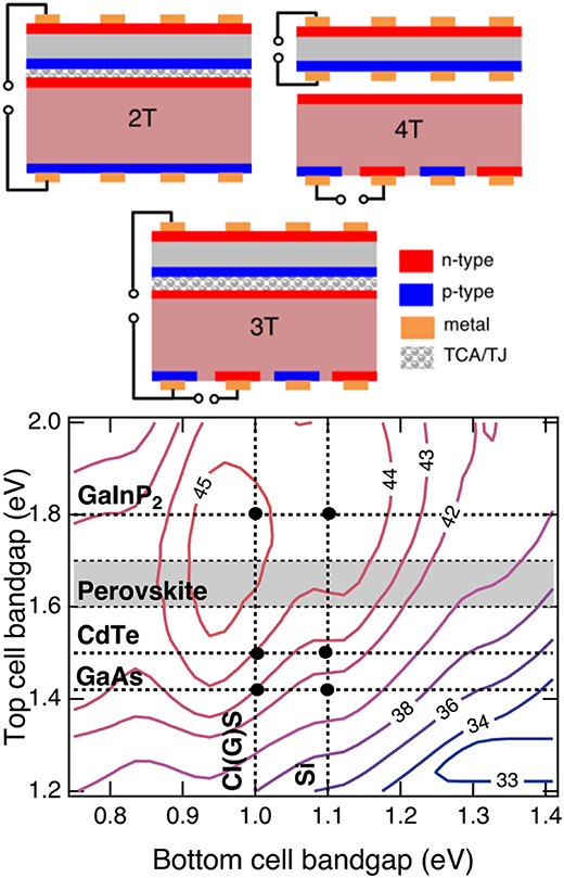
Figure 11. Top: example configurations for tandem solar cells. 2 T and 3 T cells have an electrical interconnection that can be provided by a tunnel junction (TJ, e.g. by monolithic growth), recombination layer, metal interconnect, or transparent conductive adhesive (TCA). Reproduced from [81] with permission from The Royal Society of Chemistry. Bottom: there are many different possible cell material combinations that can be used in tandems; this image shows the detailed balance efficiency for different band gap combinations for 3 T or 4 T designs (not constrained by current matching). Reproduced with permission from Dan Friedman and Emily Warren, NREL.
Download figure:
Standard image High-resolution image7.2. Current and future challenges
For terrestrial tandems, ultimately a lower levelized cost of electricity (LCOE) than for single junctions is desired, which means that it is crucial to achieve low cost of materials and processing along with very high efficiency. Due to the cost discrepancy between single junction and tandem PV, tandem solar cells are expected to enter the market in applications where the efficiency is of especially high value, including roof-tops as well as special applications such as vehicle integrated PV with severe space constraints and requirements for high efficiency. The need for differentiation among competing cell manufacturers might become a further stimulus for the tandem technology, driving initial adoption and scale up. Ultimately, any tandem cell is likely to be more expensive than a single junction cell, and thus efficiency higher than state of the art single junctions are required to justify a tandem approach. Figure 12 illustrates the progress of a number of cell technologies toward higher efficiency. As shown in figure 12, the only cells that have met this metric are III–Vs, III–V/Si, and perovskite/Si, meaning that any other technology needs efficiency improvements first and foremost. A key challenge is to continue this progress while retaining paths to lower LCOE.
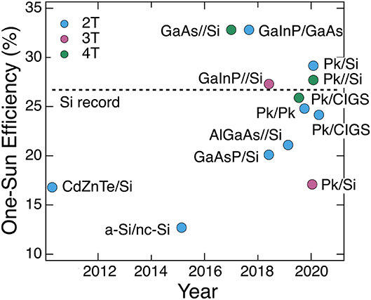
Figure 12. Highest reported efficiencies for two-junction tandem cells. Note that not all of these efficiencies are certified, and in particular, there is no established certification procedure for 3 T tandems. Materials separated by a single slash (/) represent monolithic growth/deposition, while a double slash (//) represented bonded or stacked approached. 'Pk' refers to perovskites. Only non-concentrator measurements are reported, and we have not restricted device area. Data from [72, 74–79, 82, 83].
Download figure:
Standard image High-resolution imageIn designing tandems, researchers should think beyond the individual (often small) cell level and consider how multiple tandem cells will interact in strings and modules. Two-terminal cells can simply replace existing single junctions in strings, but 3 T and 4 T designs offer higher efficiency with more complex stringing. The primary challenge for 4 T is minimizing optical and resistance losses related to lateral current collection from intermediate contacts; if this can be achieved then voltage matching of top cell and bottom cell strings enables high module efficiencies. For 3 T cells, string designs have been proposed and modelled, but more research is needed to account for the variety of device designs and integrate these findings into optimized string models [84].
Another essential component of achieving low LCOE is long module lifetime. As commercial modules are guaranteed to maintain 80% of their initial power after 25 years, this is the benchmark that we should use to evaluate silicon-based tandems. Many top cell technologies, including III–Vs and CdTe, have existing reliability track records that can be expected to apply to tandems. The stability requirements for perovskite/Si tandems have been investigated recently [85], and it was found that the maximum permissible perovskite top cell degradation rates are around 1%–2% per year. LCOE calculations indicated that if the tandem cost is 50% higher than single junctions, efficiencies of 27%–29% would result in economically competitive tandems.
7.3. Advances in science and technology to meet challenges
Because Si is a suitable material for a bottom cell, tandem technology can be applied directly to it. Current developments in the c-Si community such as local contacts and passivating contacts can be used. Options for low-resistance interconnection of the top and bottom cell include tunnel junctions between n+ and p+ doped Si layers [86], and TCOs as recombination layers, along with a new approach of direct interlayer-free connection of the top and bottom cell [87]. All of these can enable new and improved tandem cell designs. For some types of top cells deposited directly on Si, advances are needed in heteroepitaxy and nucleation both to ensure both that top cell materials can reach optimized performance and to avoid damaging the Si. This is particularly challenging given the distinct needs for Si passivation and nucleation of top cell materials. For example, III–V growth on Si generally utilizes a polished, offcut top surface, while high efficiency Si cells typically terminate with polycrystalline or amorphous materials on chemically textured surfaces. More work is needed to reconcile these distinct requirements. For thin-film based tandem devices such as perovskite/perovskite tandem cells, an improvement of the external quantum efficiency in the near infrared regime is of utmost importance [78]. For thin-film bottom cells, compatibility is required with top cell processing. Depending on the bottom cell material, this may mean improved temperature stability or altered chemical composition, in order to be resistant to solvents used in later processing steps—this is particularly important for perovskite bottom cells.
Advances in top cell materials, designs, and deposition techniques will also be required. In particular, for III–V top cells, cost reduction is the critical factor: achieving cost targets will require advances in deposition methods, substrates, and metallization, as discussed in the preceding section [72]. For perovskites, increases in efficiency and stability along with decreases in cost are required. To improve performance, greater transparency of transport materials and back contacts is required. The most important step in reducing the cost is to replace expensive materials such as gold and spiro-O-MeTAD. The number of steps in cell fabrication is also an important determinant of the cost. Promising approaches that may help to simultaneously achieve cell efficiency and stability targets are inorganic transport layers, barrier layers and new perovskite formulations.
For tandems, proper cell characterization is more difficult: it is necessary to get the right amount of light into each junction and to test stacked tandem solar cells in a fully stacked device configuration, with both cells held at load conditions, with appropriate optical masking. Erroneous results can stem from measurements differing from realistic conditions, especially via optical effects such as luminescent coupling and stray light, and underestimation of optical losses. 3 T's must be tested by measuring both circuits simultaneously, due to both optical and electrical coupling of circuits. For perovskites, hysteresis in JV curves should be considered. We need continued advances in testing and certification methodologies to keep up with new variations in cell designs.
However, researchers should not lose sight of important concerns such as scalability, module integration, and reliability by focusing too closely on small high-efficiency cells. More work also is needed in outdoor and reliability testing and modeling of strings and energy yield to have the potential to make a real impact on the market.
7.4. Concluding remarks
Tandems have the potential to allow continued reduction of the cost of photovoltaics through increasing the efficiency and hence reducing the impact of balance-of-systems costs. This has been recognized through the inclusion of silicon-based tandems in the International Technology Roadmap for Photovoltaics. If tandems are to realize their potential, they must demonstrate not only significantly higher efficiency than single junction silicon cells, but similar stability and only marginally higher cost. So far great strides have been made in the efficiency of III–V tandems, and perovskite-Si tandems have emerged recently as another promising high efficiency approach. While it is essential to continue to raise the efficiency, particularly important areas of focus now are low cost processes and materials as well as development and testing of long-term and outdoor performance. If these aims can be achieved, then tandems will become an important part of the continued cost reduction in photovoltaics and the development of solar electricity as one of the world's major energy sources.
Acknowledgments
A T's work was supported by the US Department of Energy under Contract No. DE-AC36-08GO28308 with Alliance for Sustainable Energy, LLC, the Manager and Operator of the National Renewable Energy Laboratory, with funding provided by the Department of Energy Office of Energy Efficiency and Renewable Energy Solar Energy Technologies Office under contract SETP DE-EE00034911.
R P's work was supported by the German Federal Ministry for Economic Affairs and Energy, under grant number 324 040 (project EASi), as well as by the Federal Sate of Lower Saxony.
K C's work was partly supported by the Australian Renewable Energy Agency (ARENA). Responsibility for the views, information, or advice expressed herein is not accepted by the Australian Government.
8. Non-traditional module and system designs: building integration, floating, agriculture, and flexible/high specific power applications
Matthew O Reese1 and Christopher S Klinga2
1 National Renewable Energy Laboratory
2 Architectural Solar Association
8.1. Status
Most PV is produced for utility-scale ground-mount, commercial rooftop, or residential rooftop markets. While some variations exist (e.g. current, voltage, shape), PV is generally a commodity with a 'one-size-fits-all' approach valued on a cost-per-watt basis. Silicon PV has been historically monofacial, with wafers sandwiched between glass frontsheets and opaque polymer backsheets. Thin-film modules are packaged similarly, except using glass backsheets. Increasing module size and space utilization, and reducing cell interconnection resistance have significantly reduced the cost-per-watt. The theoretical limits to improve efficiency by these methods are fast approaching. There is now focus on metrics beyond cost-per-watt. One related trend is (Si) bifacial modules which use glass or transparent polymer backsheets to absorb additional light for increased energy-yield-per-rated-watt, with reported increases up to 30% [88]. While bifacial thin-film modules exist for niche markets (e.g. solar windows), their performance suffers from higher resistance transparent back contacts. Eliminating this performance gap to enable bifacial thin-film modules is an active area of research.
While improving capacity factor, energy yield, and the value triad of efficiency, cost, and reliability will continue for the foreseeable future for 'traditional' solar, several non-traditional applications derive value on a separate axis and/or benefit from 'value-stacking'. The most common separate value axis combines flexibility and reduced weight, which go hand-in-hand. Specific power (power-to-weight ratio) is valued by aerospace (e.g. satellites, unmanned aerial vehicles (UAVs)), recreational and military person-portable, and ground transportation markets [89].
Architectural Solar or Building Integrated PV (BIPV) is the largest market (estimated ∼10 GW cumulative deployed by 2018 end [90]) presently benefiting from value-stacking (sometimes called 'dual-use'). Glass, aluminum and polymers are common materials in today's built environment while also providing photovoltaics' structural backbone. Solar's incremental cost can be reduced by directly replacing cladding elements or integrating cells into glass laminates already used within the building envelope. An appealing multi-functional attribute of photovoltaics is the opportunity to leverage its opaque or semi-transparent nature. The building industry commonly coats glass with transparent coatings (e.g. low-E) or semi-transparent patterns (ceramic frit). Both reduce the solar heat gain coefficient (SHGC) of vision or sloped glazing. Semi-transparent treatments also benefit glare control and bird-safe applications, while opaque treatments may conceal floor partitions within a façade (e.g. spandrel glass). Currently available PV technologies can address these exact needs, while also generating energy, in-turn providing a value-stack.
These 'niche' markets (figure 13) have the ability to extract additional value through alternative module and mounting architectures. These markets, while modest in size compared to utility-scale, are important due to their ability to support protected learning/experience for emerging PV players as discussed below.

Figure 13. Estimates of several non-traditional market sizes and price points. The top of each bubble corresponds to an estimate of the higher range of prices sustained in 2017, the bottom estimates potential price reductions over 10 years assuming a price reduction rate seen in the utility-scale market. The left of each bubble corresponds to a market size estimate at the beginning of the period, the right side after 20% compound annual growth for 10 years. Reprinted by permission from Springer Nature Customer Service Centre GmbH: Nature Energy [89] (2018).
Download figure:
Standard image High-resolution image8.2. Current and future challenges
For fully integrated architectural applications one size does not fit all. Glass today is a customizable architectural component and any solar-based substitutes must conform or will not be considered for integration into the building envelope. This includes not just varying transparency levels, but also the ability to specify somewhat arbitrary sizes. This presents BIPV's greatest technical challenge because of the cost implications associated with designing, manufacturing and certifying a range of sizes. Additionally, appearance is of paramount importance. Thin-film panels' homogeneity over large areas provide an advantage over wafer-based Si. Presently, while Si dominates the roof BIPV market compared to thin-films with a 90/10 market split, thin-films dominate façades with a 56/44 split [90]. The architectural glass industry is already well-versed in 'soft' coatings (e.g. sputtered low-E coatings) protected inside dual panes–replacing these with thin-film cell 'coatings' seems a logical extension. Lack of precision in manufacturing customized integrated glass units (IGUs), however, requires some technologies/designs to utilize an additional glass lite to fully seal the PV against moisture. Increased moisture resistance in thin-films could minimize these costs/relax design constraints. Another large opportunity is to utilize commoditized solar panels in place of building components. If architects adapted to a standard form factor, which sometimes happens with cladding systems, substantial costs could be avoided (figure 14). A vertical solar system costing $2–3 watt−1 (installed) at 18% efficiency, equates to $3.90–5.85 m−2. Most Aluminum Composite Material (ACM) exterior wall cladding systems common to commercial construction, have installed costs of ∼$2.75–4.65 m−2 [91]. Replacing metal cladding systems with standard, commoditized framed solar solutions present a significant opportunity to reduce BIPV costs through value-stacking.
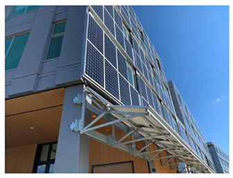
Figure 14. Traditional solar in place of metal cladding on Colorado's first net-zero multi-tenant building Boulder Commons, Boulder, CO. Photo courtesy of Christopher Klinga.
Download figure:
Standard image High-resolution imageTwo emerging value-stacking applications are floating PV (FPV), which has surpassed 2 GW installed and expects high annual growth rates with TWs of potential, and agrivoltaics (APV), which is now being explored [90, 93–95]. Unlike BIPV, the value-stacking is less straightforward to quantify and will require detailed experimental studies and new modeling.
While FPV has been most successful in markets with high land costs (e.g. Japan, South Korea, Taiwan), there is also potential to mitigate evaporation from reservoirs and/or maintain water quality, which are susceptible to undesirable processes like UV-initiated bromination and algae blooming. Furthermore, reports of FPV and APV indicate cooler operating temperatures (9 °C for APV in Arizona [95]) and hence increased performance, but no predictive model exists. A preliminary study of APV in the Arizona desert, suggests its cooler temperatures improves water-use efficiency by >150% in certain situations and improves crop yields [95]. The value associated with any storage for PV in general is not well-quantified, presenting a significant avenue of high-value research. This is highlighted by FPV installations considering co-location with hydroelectric generation, with the dual benefit of eliminating new high-power grid connections and serving as effective storage by storing water during daytime hours.
Other applications, however, require an additional value axis such as specific power and flexibility, necessitating a complete module redesign. The majority of weight and rigidity in modules stem from the package. Si wafers thicknesses range from 100–200 µm while thin-film cells are <5 µm, making the thick glass, polymer sheets, and Al framing of traditional modules an impediment to achieving high specific power. All of the traditional module's packaging elements, however, serve important roles including optical coupling; protection from breakage, mechanical loading, and water/moisture vapor; and safety against electrocution. Beyond resisting detrimental flexure, these roles can generally be accomplished with thinner, lightweight packaging substitutions (e.g. high moisture barriers films) that 'merely' cost more at today's scale than components like glass. It is worth noting, any sufficiently thinned-down material becomes flexible, with glass an excellent example. Thick glass is rigid and fragile, whereas ultrathin glass fibers are used for insulation and fiber optics. This makes it possible for any PV technology, hypothetically, to achieve high specific power, although technical obstacles pose limitations to some more than others.
It is important to note some reports overstate specific power of organic PV and perovskites, by not accounting for realistic packaging requirements/overemphasizing cell thickness. Similarly, 'half-packaged' or unpackaged cells can lead to unfair comparisons. For a detailed discussion of limitations on specific power, see [89].
8.3. Advances in science and technology to meet challenges
FPV has leveraged traditional Si panels, but innovated in mounting solutions. Mounting has largely used high density polyethylene and Al frames, with long histories in aquatic applications (e.g. buoys). Presently, reliability due to motion fatigue, soiling, and corrosion are open research questions. While systems have been fixed-tilt to date, tracking is being increasingly considered [96]. While traditional panels presently make economic sense, FPV also may benefit from membrane-based, flexible modules. BIPV's most needed technological advancement is an adaptation to cost-effectively insert PV into the glass fabrication process either as a direct soft coating similar to low-E or with a customizable laminate (e.g. thin-film structure on polymer adhered inside glass)–either must have a solution for arbitrary sizes.
Each high specific power PV technology presently has a drawback. While 150 µm thick Si wafers make efficient solar cells and are more flexible than 200 µm ones, they are still fragile and heavy compared to thin-film absorbers. Ultrathin (<10 µm) Si is highly flexible, but silicon's indirect bandgap makes light harvesting more challenging and research is needed to reduce its significant interface recombination, with efficiencies less than half of Si records [97]. The most efficient polycrystalline thin-films (CIGS and CdTe) are deposited at temperatures incompatible with the lightest weight plastic substrates. This requires altering processing conditions, which often lowers efficiency. Potential research directions include flexible glass or metal substrates, which can introduce different impurities and thermal mismatch or a liftoff approach, with issues in cracking and impurities [98–103]. Perovskites and organic photovoltaics have the lowest thermal budgets, making growth on plastic substrates more straightforward. However, they still use transparent conducting oxides (TCOs), with limited flexibility before fracture. Metal (nanowire) networks and TCOs with metal interlayers are being explored as flexible replacements. This element must be improved or controlled for, by setting limits to flexure into a final package design. High moisture barriers will also be required for the near future, and lowering their cost-per-performance can boost these niches. III–V PV's challenge is reducing cost without losing efficiency to maintain its dominance in the highest specific power applications.
Additionally, further technical challenges in aerospace, person-portable, and vehicle-integrated PV applications cost are balancing specific power with reliability. Aerospace is the least cost-sensitive (up to $100–200 W−1) due to the high launch and system costs (although these are dropping), but with added reliability to temperature/pressure cycling and radiation hardness, while relaxing the actual required operational lifetime (i.e. 1–5 yr for UAVs, 1–8 yr for low earth orbit, 7–15 for geosynchronous orbit) [89]. Vehicle integration for range extension of plug-in hybrid and battery electric vehicles is the most cost-sensitive ($2.5–10 W−1) application, with appearance also critical and reliability linked to car lifetime (i.e. 250 000 miles or 10 yr) and crash safety standards [89]. Person-portable PV has intermediate specific power and cost-sensitivity ($4–16 W−1) requirements, with greater durability to rough handling, but relaxed operational lifetime requirements (1–3 yr) [89].
8.4. Concluding remarks
As many of these applications have been previously considered, a natural question is why are they still 'niche'? Despite the added value-stack benefit, especially now with plummeting PV component costs, there are still major barriers to widespread adoption. For BIPV these are: lack of building industry buy-in to integrate solar technologies; codes and standards geared towards standardized products rather than customizable architectural solutions; and an uneducated market on how to integrate such technologies. Floating PV, though growing exponentially, is in the infancy of understanding siting, reliability, and quantifying its value-stack. Numerous companies have pursued lightweight, flexible PV products for many years. To date, a value proposition trade-off has limited each market's size. Some cost limitations stem from the added price of customization. Even c-Si products at low-scale cost an order of magnitude more than utility-scale. The special requirements of these markets maintain them as laboratories of innovation. To date they have supported every commercialized technology (a-Si, c-Si, CIGS, CdTe, OPV, DSSC, III–V), with the advances of each pushing the whole market. These markets' prospective value has the potential to support billions of dollars of experience, which can ultimately lower costs. This can lead to the implementations of new technologies and architectures at large-scale, which may find new value propositions beyond the lowest upfront cost-per-watt.
9. The role of storage in multi-terawatt-level PV integration
Paul Denholm1 and Mahesh Morjaria2
1 National Renewable Energy Laboratory
2 First Solar Inc.
9.1. Status
Very-large-scale deployment of PV will require addressing the variable and uncertain nature of the solar resource. Lessons learned from current levels of PV deployment, and studies of even higher levels of deployment in many regions, have helped clarify the pathway towards cost-effective integration of PV at the multi-TW level and the role of 'enabling' technologies such as energy storage.
Overall, the challenges of integrating PV occur at multiple timescales and change in nature as PV penetration increases. Early concerns regarding deployment at low penetration (up to a few percent on an annual basis) focused on the short-term variability of PV and the potential for output to drop rapidly in the seconds to minutes time frame. This concern has been largely mitigated by factors including recognizing the impact of spatial diversity, which greatly reduces aggregated PV ramping events in this short time frame [104]. Other measures have enabled cost-effective PV integration, such as improved market operations including increasing size of the balancing area, enabling sub-hourly scheduling and dispatch, improving forecasting, and increasing power system flexibility [105]. Some of the needed flexibility can also be derived from PV itself, by dispatching it to provide operating reserves and by taking advantage of the extremely rapid response rates available from inverter-based resources, as opposed to thermal resources that take much longer to respond [106].
9.2. Current and future challenges
As PV penetration increases further, the diurnal mismatch of supply and normal electricity demand patterns becomes a greater concern. This mismatch includes both the potential oversupply of PV during periods of relatively low demand, and insufficient PV generation during periods of high demand. These issues are commonly illustrated by the 'duck curve,' shown in figure 15, which shows periods of low net load and potential overgeneration (resulting in PV curtailment) that has started to occur in places such as California on some spring days [92]. During periods of low demand, a combination of large PV generation and flexibility limits on current power plants results in generation that exceeds demand. During these periods PV must be curtailed, which decreases its net capacity factor, increasing its cost of delivered energy (or decreasing its value, depending on perspective). This decline in PV energy value as a function of penetration is compounded by its decline in capacity credit, or its ability to replace conventional generation resources that are typically available during periods of peak demand (sometimes simplistically described as dispatchable or 'firm' resources) [107]. In the USA, and in many other regions with warmer climates, the demand for electricity peaks during hot summer afternoons that are often coincident with high solar output. However, as PV is added, the net peak demand is shifted to later in the day during periods of low output. This means that even at relatively low penetration (<20% on an annual basis) PV by itself may provide little incremental contribution to a system's ability to meet its peak demand. In combination, these factors decrease the cost competitiveness of PV and will require measures to improve the diurnal coincidence of solar supply and energy demand.
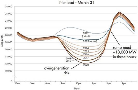
Figure 15. The California 'duck curve' showing both the challenge of potential overgeneration and high net load ramp rates at sundown . Reproduced with permission from [92]. Licensed with permission from the California ISO. Any statements, conclusions, summaries or other commentaries expressed herein do not reflect the opinions or endorsement of the California ISO.
Download figure:
Standard image High-resolution imageBeyond the diurnal mismatch, there is a seasonal mismatch that varies regionally. In summer-peaking systems, this mismatch can be relatively small; however, in many regions of the world, demand can peak during the winter or other periods of low solar output.
9.3. Advances in science and technology to meet challenges
The declining value of PV can be partially mitigated by many cost-effective non-storage options. These include increased power system flexibility, which can be enabled by improved PV forecasting and power system scheduling. Greater use of flexible loads could substantially address the issue of supply/demand imbalance. Lower-cost PV can help mitigate the decline, as cheaper PV can remain cost effective even with the lower capacity factors that result from curtailed energy [108]. Lower-cost PV also allows for higher DC/AC ratios that have reduced variability and greater output during shoulder periods in the evening. Addressing the diurnal supply/demand mismatch is the first step in enabling extremely large-scale PV deployment.
However, there are of course limits to what low-cost PV can achieve by itself, given the simple unavailability of solar energy at night. Science and technology advances are critical to develop practical storage solutions for diverse PV applications. Compressed air, flywheels, supercapacitors, and solar-to-fuels such as hydrogen have been discussed for some time, but still require development. In 2017, pumped hydro had a total nameplate capacity of over 180 GW, accounting for 95% of tracked storage installations worldwide [109]. Pumped hydro energy storage systems borrow technology from hydroelectric power generation systems and have been in service for over 70 years. In these systems, water is moved from a low elevation reservoir to a higher elevation reservoir during periods of low demand, and then the flow is reversed to drive turbines during periods of high demand. Energy can be stored for days or even weeks depending on the size of the system. Drawbacks include high initial capital investment and geographically unique locations. Positives include high system reliability, multi-decadal service life and round-trip efficiency of ∼80%. Recent work suggests that geographical limitations may be less of a barrier for modern off-river pumped hydro facilities that make use of deep reservoirs with large large elevation differences and the use of brown field sites and decommissioned mines [110].
Diverse battery technologies can also help meet storage challenges. The outstanding energy capacity of lithium-ion batteries coupled with enormous cost reduction has been displacing the traditional lead-acid battery. Lithium-ion batteries have seen a nearly 90% reduction in prices in real terms from $1183 kWh−1 in 2010 to $156 kWh−1 in 2019 and is expected to approach $100 kWh−1 by 2023 [111]. One challenge is to scale battery technologies to levels appropriate for TW deployment, and at the same time develop particular anodes, cathodes, electrolytes, battery controls, and plant management with properties tailored specifically to PV applications. Solar panel warranties are typically 25 years and likely to become longer, so a key challenge is to develop battery technology that can retain high round trip energy efficiency for more than 9000 cycles with suitable power charging and discharging rates within cost constraints that will enable PV + storage to be significantly less expensive than conventional electricity sources.
In the near term, relatively short-duration storage (4 h or so) can mitigate much of the overgeneration concern [112]. In addition, PV physically coupled with short-duration batteries (∼4 h) creates a unique synergy that enhances grid capability of a PV plant (e.g. capacity firming, energy shifting, and flexibility) and makes it competitive with new peaking capacity [113]. When storage and PV are physically coupled and share a common interconnection and infrastructure, the project cost savings are realized. Systems coupled on the DC side of a shared inverter can enable higher DC/AC ratios, which can further reduce project siting and other balance-of-system costs. With respect to policy, the US Income Tax Credit incentive has motivated many developers to include storage with PV. These project savings in turn reduce cost per unit of delivered energy.
As PV penetrations increase, longer-duration storage can largely address the requirements for diurnal shifting—and studies have found that batteries or other storage technologies with eight or less hours of capacity can achieve economic penetrations of PV greater than 50% on an annual basis [114]. Figure 16 (top) illustrates a modelled projection scenario demonstrating the possible deployment under further aggressive cost reduction (achieving 3 cents kWh−1 by 2030 for utility- scale PV in average locations in the USA). It also shows the impact of advancing lower cost storage, which greatly increases deployment. Figure 16 (bottom) illustrates how storage could be dispatched to shift supply to evening and early morning.

Figure 16. Deployment scenario for PV in the United States under an aggressive cost reduction target, and also with low cost storage (top). Dispatch in the Western and Eastern interconnections during periods of highest instantaneous penetration of nonsynchronous generation. Source: NREL.
Download figure:
Standard image High-resolution imageAt ultra-high PV penetrations (>50% on an annual basis), longer-term (including seasonal) mismatch may drive declining PV economics. Shifting energy supplies over days, weeks, or months may be needed depending on the region. Development of advanced 'conventional' longer-duration storage technologies, including pumped hydro and compressed air energy storage, may enable the multi-day shifting requirements, while the focus of truly seasonal storage has been the conversion of electricity to storable fuels for later use in fuel cells or thermal generators. For purely electric applications, existing non-battery technologies are limited by low round-trip efficiencies [115]. However, solar fuels production also enables economy-wide decarbonization by providing transportation fuels, space and process heating, and chemical feedstocks. Understanding the trade-offs among competing storage technologies requires additional analysis, including examining the potential role of meeting seasonal mismatch through using PV as a purely 'peaking' resource with very low net capacity factor. Ultra- low-cost PV potentially allows for 'overbuilding,' which can generate greater production during peak seasonal periods, while accepting greater amounts of cost-effective curtailment during periods of low demand. The economically optimal configuration of systems with very large amounts of PV has not been well characterized, given the evolving state of the technology.
9.4. Concluding remarks
Multi TW-scale PV deployment ultimately requires addressing the inherent mismatch between when the sun shines and when people use energy. The short-term (sub-hourly) mismatch problem can be largely addressed via changes in how the grid is operated. The diurnal mismatch challenge will likely require deployment of a variety of technologies, including storage with multiple hours of capacity, to ensure the peak demand for electricity can be served. On longer timescales (12 or more hours), the challenge becomes more difficult due to the high capital costs, low efficiency, and low utilization rates of storage, which decreases the economic competitiveness of PV. A research agenda to improve the cost and performance of storage technologies at all timescales will aid in finding solutions to achieve extremely high PV penetrations.
Acknowledgments
This work was authored in part by the National Renewable Energy Laboratory, operated by Alliance for Sustainable Energy, LLC, for the US Department of Energy (DOE) under Contract No. DE-AC36- 08GO28308. Funding provided by the US Department of Energy Office of Energy Efficiency and Renewable Energy Solar Energy Technologies Office. The views expressed in the article do not necessarily represent the views of the DOE or the US Government. The US Government retains and the publisher, by accepting the article for publication, acknowledges that the US Government retains a nonexclusive, paid-up, irrevocable, worldwide license to publish or reproduce the published form of this work, or allow others to do so, for US Government purposes. Editing support was provided by Devonie McCamey.
10. Energy yield modeling
Michael G Deceglie1, Janine M Freeman1 and Mark A Mikofski2
1 National Renewable Energy Laboratory
2 DNV GL
10.1. Status
Modeling PV energy yield is crucial throughout the value chain for designing and financing projects, investigating new technologies, identifying underperforming systems, and understanding how PV fits into energy infrastructure. Reliable models with accurate inputs and well-quantified uncertainties enable successful deployment and shorten financial negotiations, decreasing overall costs. Established methods for predicting system yield in real world conditions have been an important component in the expansion of PV. However, there are also opportunities for continued advancement to support rigorous design optimization, improved uncertainty analysis, emerging technologies, and more challenging conditions like complex terrain.
A great deal of progress has been made with current practices employing modelling software with a single year of hourly solar resource and weather data (e.g. typical meteorological year (TMY) [116]) and system characteristics (e.g. PV temperature coefficient) to predict energy yield. A complete model is built from sub-models for each step of the conversion from irradiance to module performance to system energy output [117]. For some of these steps, there are established models with accepted uncertainties, but others rely on estimates resulting in high uncertainty. Even well-established models have only been validated against limited data.
10.2. Current and future challenges and advances in technology to meet them
10.3. Model inputs
Solar resource availability is one of the largest predictors of energy yield, but estimating it for a specific location is challenging. The status quo is to use a single year of hourly resource data. This practice became prevalent partially to overcome challenges with limited computational power [116]. The development of satellite-based irradiance models has improved the geographical and temporal extent of available irradiance data. This, along with increases in computing power, provide the opportunity to model at higher temporal and spatial resolution, and to improve methods of utilizing many years of historical data to better understand uncertainty in PV yield. As shown in figure 17, higher frequency simulation (e.g.: minutes or seconds) enables models to accurately capture sub-hourly clipping and ramp rates, effects that hourly modelling does not capture, for more accurate predictions. Synthesized high-frequency data [118] could provide a promising solution with adequate validation against appropriate ground data.
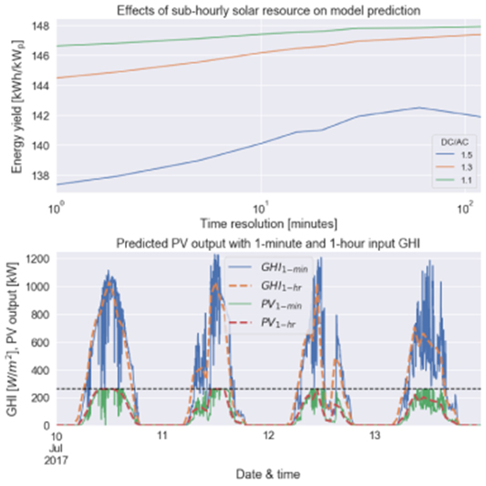
Figure 17. High-frequency solar resource data from the NIST testbed [119] was used to predict energy yield for three hypothetical systems with different DC/AC ratios of 1.1, 1.3, and 1.5 based on the NIST ground array for the month of July. Top panel shows modelled energy yield for systems with different DC/AC ratios as the time resolution of the solar resource data is changed. Down-sampling data from 1 min to 2 h shows energy yield is over-predicted when DC/AC ratio is high, but as DC/AC ratio approaches unity, predictions are less sensitive to data-resolution. Bottom panel shows a subset of several days of global horizontal irradiance (GHI) resource data and the resulting modelled PV system output (PV) for one-minute and 1 h time resolution, with a DC/AC ratio of 1.5. The DC/AC clipping limit is indicated by the dashed horizontal line. Intermittent high solar resource is not captured by hourly data resulting in under-predictions of clipping loss and an over-prediction of energy yield.
Download figure:
Standard image High-resolution imageThe single diode model used to predict module power output results in additional input complexity. It requires parameters that cannot be directly measured from cells or modules. Multiple methods exist [120, 121] to derive these parameters from measured characteristics under varying temperature and irradiance, but industry has not converged on the most accurate method. Public databases of module characteristics (e.g. IEC 61 853 matrix data) paired with field performance data would aid in building industry consensus.
Losses and their uncertainty must also be considered. Examples include degradation, snow, soiling, and equipment outages. Solutions like SAM's PV-RPM [122] offer a promising approach to quantify losses and their uncertainty. Such approaches require good input about the probability and impact of different losses. The development of promising new analysis tools such as StatisticalClearSky [123] and RdTools [124] along with fleet-scale analyses like the PV Fleet Data Initiative [125] may offer the opportunity to quantitatively understand losses at scale and close the loop with developers, independent engineers, and investors.
10.4. Meeting the demands of advancing technology
In order to gain traction with stakeholders, models for emerging technologies must be credible and accurate. For example, the industry is grappling with modeling bifacial systems, due in part to a dearth of high-quality, realistic, independent validation datasets from large-scale bifacial systems. There is much uncertainty around bifacial gain, its effects, and optimization. Advances in modelling are still required to understand whether energy yield gains justify the cost of bifacial modules. Currently, bifacial gain is quantified with two-dimensional view factor models that assume infinitely long arrays. Recent advances in raytracing and cloud computing [126, 127] have enabled models that treat electrical mismatch, structural shade, and transmission. However, these simulations are slow and expensive, making them intractable for practical use. The challenge is to create fast and accurate modeling tools to both predict and optimize bifacial performance. Similarly, there is a need for improved modeling and optimization of single axis trackers and their tracking algorithms for both bifacial and monofacial systems.
Bifacial modules illustrate the importance of laying the groundwork for accurate energy yield modeling for new and emerging technologies. This includes looking beyond standard test condition (STC) measurements and record cell efficiencies for emerging cell technologies like perovskites and tandems. It is useful to characterize cells under varying temperature, irradiance, and spectrum, then to use this data to quantify energy yield potential in the field. It is also important to realistically consider how the technology will be interconnected in modules at the square-meter scale and consider associated losses. Finally, as the technology matures and full-size modules become available, realistic research-grade field performance data should be collected and scrutinized by the community to build confidence in associated models.
Models must also evolve with the rest of the power system. As increased renewable penetration drives PV-coupled battery storage, models must consider the complexities of systems with storage. Modeling challenges include DC- vs AC-connected topologies, complex degradation, thermal and voltage characteristics, and rapidly evolving value streams. Additionally, modeling battery dispatch is essential to estimating system value, and involves assumptions about generation and load forecasting. Many PV modeling tools have already added the ability to couple PV systems with battery storage, but development and evolution of these models will need to continue to keep pace with the rapidly changing battery market.
Similarly, with increased renewables on the grid, PV plants will no longer operate simply to maximize energy output, but may be required to provide grid services or work within voltage, frequency, and reactive power constraints. These new behaviors need to be included in energy yield models. This will require new complexity in inverter models and may precipitate coupling detailed PV models with distribution or transmission grid models to fully understand complex interactions.
10.5. Validation, uncertainty, and optimization
An important challenge is validation of model accuracy against measured data, especially for new and emerging technologies. Proper validation requires high-quality, relevant, large-scale, clean, and documented datasets. Although some entities have sufficient proprietary data to conduct internal validations, public datasets provide greater reproducibility and can accelerate adoption of new models. There exist some high-quality datasets such as the mobile performance and energy rating testbed mPERT [128] and NIST [119] datasets, but datasets for large systems are limited. More publicly-available datasets of this high caliber, especially for large-scale systems and emerging technologies, will accelerate the development of better, faster, more accurate models.
Uncertainty is present in every aspect of PV modelling, and it affects many financing decisions. Yet the industry lacks transparent, widely accepted methods to quantify uncertainty in energy yield estimates. Better definitions of terms and more robust methodologies will help build consensus and standardize the calculation of this critical metric in energy yield modeling.
Furthermore, as more and more PV systems are deployed, the need for automated optimal system design increases. Many developers still design systems manually, using CAD tools and rules of thumb, instead of coupling design to performance. No longer are systems exclusively installed on graded land in the desert southwest; new systems are located in rolling terrain, in areas with high snowfall, or with a new focus on rear-side irradiance. These novel system environments call for true design optimization, which is only achievable through accurate modeling of new and existing technologies. Cloud computing power and open source software provide new opportunities to optimize these systems for energy, cost, and construction.
10.6. Concluding remarks
As the PV industry advances in both applications and technology, so too must energy yield predictions. We have described several areas for continued advancement. Those are briefly summarized here:
- Good models begin with good inputs. Moving away from hourly single-year data to high-frequency multi-year weather datasets along with improved understanding of model inputs, losses, and uncertainty will yield more accurate, higher-confidence models.
- PV remains a rapidly evolving space, with new cost-reducing and value-increasing ideas emerging regularly. From novel cells to bifacial technology, tracker algorithms, energy storage and more, each technological improvement demands an accurate and timely representation in the modeling world to ensure its success.
- Models are only as good as our ability to validate them. High-quality public validation datasets, relevant to current technology trends (e.g. bifacial systems) are critical to building industry consensus around evolving models and their inputs.
- Finally, advances in cloud computing power and open source software provide a tremendous opportunity to move energy yield modeling beyond prediction and into optimization to improve the value proposition of PV and unlock new applications.
Each of these challenges presents a unique opportunity for the PV modeling world to enable the continued success of the PV industry.
Acknowledgments
Funding provided by the US Department of Energy's Office of Energy Efficiency and Renewable Energy (EERE) under Solar Energy Technologies Office (SETO) Agreement Numbers 34 348 and 34 221.
11. PV reliability
Dirk C Jordan1 and Govindasamy TamizhMani2
1 National Renewable Energy Laboratory
2 Arizona State University
11.1. Status
Reliability plays a central role in PV project economics and the cost competitiveness with traditional energy sources. Early reliability efforts for terrestrial applications originated from the Jet Propulsion Laboratory (JPL) Flat-Plate Solar Array project, which colloquially became known as the JPL Block Buy program. State-of-the-art modules from commercial manufacturers were purchased, tested, and fielded. Feedback of the detailed observations were provided back to the manufacturer for product improvements. Starting in 1975, through five rounds, the failure rates were drastically reduced and longevity considerably increased [129]. Beyond these obvious reliability improvements, the program had a lasting impact on the industry. Many of the tests that constitute the International Electrotechnical Commission (IEC) 61215 PV module qualification standard—and its predecessor, the Commission of European Communities (CEC) Specification 503—are based on the tests first developed during that time period [130]. This qualification standard is a set of tests that quickly expose design or materials flaws that would otherwise lead to premature failures (infant mortality) in fielded modules. Yet, these tests are not designed to provide information about life expectancy. The sustained commercial success, however, depends on the performance of a module and system to within expectations over its entire life.
This reliability challenge is visualized in figure 18, which shows the exponential growth of installed PV capacity—in gigawatts direct current (DC)—from 1976 to 2019 (blue diamonds) [131]. The consequence of this often-discussed growth curve is shown in the red circles, which is the percentage of PV capacity installed for less than 2 years. These numbers are derived from the growth curve alone and do not include decommissioning of systems that have reached their end of life. When the industry was in its infancy during the 1970 s and 1980 s, about three-quarters of all installations had been installed for less than 2 years. That high percentage was less of a concern because the longest warranties ranged from 1 to 3 years. During the following decades, the percentage of systems fielded for less than 2 years first declined and then rebounded to around 40% at the time of this writing. However, the length of warranties increased disproportionally to a range of 25–30 years. This spread between guaranteed performance and field time adds to the challenge of PV reliability.
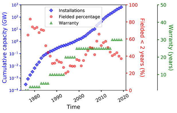
Figure 18. Cumulative installed PV capacity from 1976 to 2019 (blue, left axis). Percentage of installations installed for 2 years or less (red, right axis) and longest warranty (green, rightmost axis).
Download figure:
Standard image High-resolution image11.2. Current and future challenges
Two macrotrends have dominated the PV industry throughout its existence: (1) downward price pressure leads to the introduction of new materials and processes; and (2) cell and module designs continue to increase in efficiencies. The consequence of these two trends is a technological landscape that is continually changing, which potentially impacts PV failures and degradation. Typically, failures are sudden terminations of production or precipitous reduction in performance below a specified threshold (e.g. the warranty). On the other hand, degradation—also known as soft failures—is the gradual, relative loss of performance, which may eventually lead to failure [48]. Degradation rates, or curves for non-linear cases, are typically low—about ½ to 1% per year, and the rates are a relative number and should not be confused with the absolute efficiency of a cell, module, or system. For instance, if a module that has an initial absolute efficiency of 22%—a high-end module today—steadily degrades 0.6 relative percent per year, it would still have an almost 19% absolute efficiency 25 years later. Minimizing both degradation and failures is essential for the bankability of PV.
Historically, cell, module, and system reliabilities have been separated because module reliability issues have primarily concerned module packaging (e.g. encapsulation discoloration, delamination, broken glass and cells, and solder-bond failures), which were differentiated from cell-related issues. The situation has changed substantially during the last decade. Module packaging can still be problematic, especially with the introduction of new materials such as encapsulants or backsheets; but in addition, cell-related reliability issues can have an impact in the early-life phase such as LID or LeTID [132]. Cell design-related reliability issues are also beginning to emerge in long-term field observations [133]. Furthermore, new module designs, such as half-cut cells to reduce series resistance, shingled cells, bifacial modules that can also capture light reflected from the rear, and glass-glass construction, may lead to the emergence of new failure and degradation modes.
System-level innovations, such as higher operating voltages, have led to potential-induced degradation (PID) that impacts PV reliability [134]. In addition, increased usage of trackers, which lead to higher operating temperatures and higher inverter loading ratios (DC to AC ratio), may also impact PV reliability. Furthermore, new applications such as floating PV (systems built on water instead of land) may provide reliability challenges. Despite these challenges, reported module field failures in recent years have been relatively low compared to other PV system components such as inverters, perhaps due to the PV reliability learning cycle shown in figure 19. However, further improvement in reliability is a key, as new technologies such as PERC are fielded.
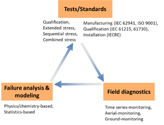
Figure 19. The PV reliability learning cycle for continuous improvement aims to maintain quality despite continuous changes.
Download figure:
Standard image High-resolution imageUntil now, decommissioning and recycling of older PV systems has been relatively low; however, the numbers of systems reaching their end-of-life state may increase in proportion to the installation growth curve. Therefore, the demand for a circular economy may also introduce new cell designs, materials, and processes into the PV value chain, with perhaps new challenges for PV reliability.
11.3. Advances in science and technology to meet challenges
The PV reliability learning cycle is a continuous improvement cycle that starts with observation and diagnostics of fielded products. Understanding of the underlying degradation mechanisms through failure analysis allows to develop physical models of the mechanism. These models then can be used to develop accelerated tests that can be applied to new products. Subsequently, products that have passed tests developed for this degradation mechanism can be fielded with higher confidence, thus closing the learning cycle. Unfortunately, the length of each learning cycle (years) is considerably longer than the product development cycle (months).
Improving PV reliability depends on reducing the reliability learning cycle. Multiple degradation or failure mechanisms may be occurring in parallel or series in PV modules. In addition, indoor accelerated tests may be unintentionally accelerating a failure mechanism that may not be observable in the field. Therefore, accurate field observation and detection are a critical part of the feedback loop. As the cost of data storage, acquisition, and processing continues to decrease more granular and richer datasets are becoming available and are providing the opportunity to determine field changes more quickly. In particular, the advent of machine-learning algorithms and cloud-computing will allow for more detailed and faster analysis of time-series datasets and real-time alerting, thus shortening the feedback loop.
Additional ex-situ methods, preferably contactless as to not interrupt production (such as electroluminescence, photoluminescence, or ultraviolet fluorescence) allow multi-dimensional characterization of the physics and chemistry within a module. When these techniques are combined with aerial vehicles such as drones the integrity of large installations can be quickly investigated. Complementary minimally invasive ground techniques such as reflectometry may quickly detect interruptions.
Further reduction in the reliability feedback loop may be achieved through in-situ monitoring the continued miniaturization of physical and chemical sensors allows the possibility to embed sensors in modules, thus enabling more rapid identification of changes within a module [135]. Because of the added cost, embedding sensors in a majority of modules may be impractical for the foreseeable future. However, these sensors could be embedded in only a few modules that would serve as 'control' modules. These control modules in the field could be stressed and the degradations could be accelerated at higher temperatures through the use of thermal insulators covering the substrates of the modules. Changes inside these modules could lead to more rapidly identifying problems and a proactive approach to operations and maintenance. In addition, it would also lead to more quickly identifying degradation mechanisms such as PID and developing physical and chemical models to accelerate the learning curve of degradation science.
These degradation models could then lead to more rapid development and implementation in extended, sequential and combined stress tests, thus closing the reliability learning cycle [136, 137]. Chemical sensors in a module may alert to changes in the chemistry such as the presence of acetic acid, which may indicate changes in the encapsulation. In addition, sensors could alert to the presence of hydrogen, and thus, to diffusion of hydrogen, which is often used in advanced cell architectures. Physical sensors may detect changes when delamination occurs or excessive impacts from snow, wind, or hail.
These enhanced characterization methods and understanding can further help guide materials science solutions. For example, nanomaterials provide exciting opportunities to improve PV reliability. For instance, embedding carbon nanotubes or other nanomaterials in the metallization may help preserve electrical integrity even when cell or interconnection cracks occur that would typically disrupt current extraction [138]. Other material science opportunities are not limited to the cell and module level but are also at the system level. For instance, inverters have been found to be the balance-of-system component that has failed most often in PV systems. Advances in developing wide-bandgap semiconductors could lead to more efficient inverters, and thus, reduced heat-dispersion requirements and potentially more robustness to elevated temperatures.
11.4. Concluding remarks
Reliability is of the utmost importance for the bankability of PV and its cost competitiveness with traditional energy sources. The PV industry often guarantees multiple decades of performance, which can be difficult to predict in a short timeframe. The challenge and the future of PV reliability is to shift from a more reactive approach to a more proactive approach by reducing the length of the PV reliability learning cycle. The convergence of multiple scientific disciplines at the cell, module and system level is required to achieve that goal in this dynamic environment.
Acknowledgments
The authors would like to thank Teresa Barnes, Don Gwinner, and Katherine Jordan for helpful discussions.
12. PV materials and device characterization
Dana B Sulas-Kern and Mowafak Al-Jassim
National Renewable Energy Laboratory
12.1. Status
Photovoltaic (PV) energy conversion is achieved through a wide range of technologies with varying active materials, processing treatments, device configurations, packaging schemes, stages of development, and intended uses. In this dynamic field, the quest to optimize photovoltaic devices does not imply only one ideal final configuration. For example, robust devices suited for floating PV installations (i.e. resistant to salt corrosion, water ingress, waves, and high winds) are likely not the same as the light and flexible systems chosen for mounting onto low-weight-capacity or mobile structures. These varying needs of end users, and the impressive range of available PV technologies, simultaneously complicate and enrich the task of characterizing PV materials and devices.
Ultimately, PV efficiency is judged by the photodiode current-voltage (I–V) response, but I–V characterization alone is insufficient to comprehensively understand the underlying physical reasons for differing PV performance and reliability. Figure 20 illustrates some elements of the diverse toolset employed to examine PV materials, ranging from (a) analysis of module power output and degradation rates [139], to (b) international standard test protocols for early identification of field-relevant failure mechanisms [140], to (c) nano/microscale analysis of defects and atomic structure [141], to (d) optical probing of energy landscape and excited-state quasiparticles [142]. As PV technologies mature and bankability gains importance, the mix of characterization methods correspondingly evolves. In particular, increasing cell sizes, incorporation into meter-scale modules, and deployment of PV arrays increases the need for spatially-correlated measurements that link the distribution of fundamental materials parameters to the efficiency of charge generation and collection, enabling targeted optimization of the entire PV package.
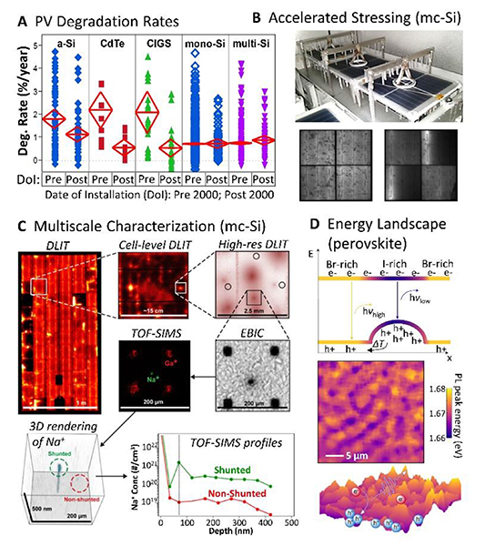
Figure 20. Examples of PV characterization including: (a) statistical analysis of current-voltage parameters from [139], where this study shows degradation rates of module power output for various technologies from pre- and post- year 2000, collecting data from over 100 publications and 32 countries; (b) in-situ electroluminescence imaging during combined-accelerated stress testing from [140]; (c) multiscale, multi-method characterization ranging from module to atomic level, in this case using dark lock-in thermography (DLIT), electron beam induced current (EBIC), and time-of-flight secondary ion mass spectrometry (TOF-SIMS) to identify Na+ accumulation causing shunting during potential-induced degradation from [141]; and (d) luminescence imaging allowing to make structure-property relationships between chemical composition and energy landscape, in this case for perovskite devices from [142]. (a) [139] John Wiley & Sons. Copyright © 2013 WILEY-VCH Verlag GmbH KGaA & Co., Weinheim. (b) © IEEE. Reprinted, with permission, from [140]. (c) [141] John Wiley & Sons. Copyright © 2018 WILEY-VCH Verlag GmbH KGaA & Co., Weinheim. (d) Reprinted by permission from Springer Nature Customer Service Centre GmbH: Nature Photonics [142] (2018).
Download figure:
Standard image High-resolution imageWithin the varied PV characterization toolset, methods are needed for characterization from size scales of meters down to angstroms, where the structural and chemical materials properties would ideally be correlated to the electro-optical performance. Optical characterization often has the practical advantage as being relatively simple and non-destructive for probing defect states, variations in crystallinity/phase/composition/purity, and degradation of material or interface quality over time. However, other types of probes can offer greater spatial resolution, such as electron beam-based measurements (e.g. scanning electron microscopy, SEM; transmission electron microscopy, TEM) or using an oscillating sharp tip (e.g. atomic force microscopy, AFM). Both destructive and non-destructive probes can also be used for characterizing chemical composition (e.g. sputtering paired with methods like x-ray photoemission spectroscopy, XPS and secondary ion mass spectrometry, SIMS). Here, we discuss some challenges for PV characterization and how a mix of multiple methods with reasonably high through-put is needed for comprehensive multiscale analysis.
12.2. Current and future challenges
12.2.1. Multiscale characterization for cell and module development.
Multiscale and multi-technique characterization of PV materials and devices is both necessary and challenging. In addition to tracking nonuniformities from the module level down to the sub-cell or nanoscale materials level, some challenges for commercial-level PV module characterization include: accessing active cell components within the module packaging for microscopic characterization; distinguishing between module-scale packaging/interconnect degradation versus cell-level properties; quantifying the relative importance of identified defects; differentiating between design flaws versus poor manufacturer processing; making characterization higher throughput and more accessible to non-specialists; and developing outdoor-compatible instrumentation implementable without disrupting field operations.
12.2.2. Electro-optical characterization.
Electro-optical characterization can be performed over large spatial scales, and these methods are essential for optimizing PV electricity generation from materials' interactions with light. However, at the lower limit, the spatial resolution of optical methods is restricted by the diffraction limit of light (i.e. hundreds of nanometers to micrometer scale). Although impurities, defects, or other structural features causing low-energy trap states may be significantly smaller, optical methods (such as time-resolved photoluminescence, microwave photoconductivity, transient absorption microscopy, Raman, Fourier-transform infrared spectroscopy, reflectance, etc) provide important information about thermodynamics and kinetics affecting photovoltaic operation that could not be inferred from structural characterization alone. For example, carrier lifetimes are inherently related to voltage, and time-resolved absorption/emission spectra can provide information about excited state occupancy. For these reasons, optimization of electro-optical characterization methods is needed despite the poor lower-limit of spatial resolution.
12.2.3. Microscopic structural and chemical characterization.
On smaller spatial scales, structural characterization methods have been well-developed and can achieve nanometer (e.g. AFM, SEM) to angstrom (e.g. TEM) levels as shown in figure 21. For PV materials characterization on these size scales, the greater challenge lies in the ability to correlate spatial properties with atomic composition or the lower-resolution electro-optical characteristics. Methods for detecting elemental concentrations are typically only sensitive to 0.1–1 atomic percent. This includes STEM-based methods such as electron energy-loss spectroscopy (EELS) and energy dispersive x-ray spectroscopy (EDS) that offer nanometer spatial resolution, or time-of-flight-SIMS with 100 nm resolution. Higher chemical sensitivity can be obtained with dynamic SIMS, but the improvement in sensitivity comes with decreased spatial resolution, e.g. from ∼100 nm for TOF-SIMS to ∼1 µm or more for d-SIMS. Due to the difficulty in characterizing the composition at the atomic scale, many studies rely on prior knowledge of the different materials that were used during fabrication. This strategy has been used, for example, for inferring the role of hydrogen in light and elevated temperature induced degradation (LeTID) in silicon cells [143]. However, prior knowledge of the bill of materials is not often a viable strategy during studies of commercialized devices.

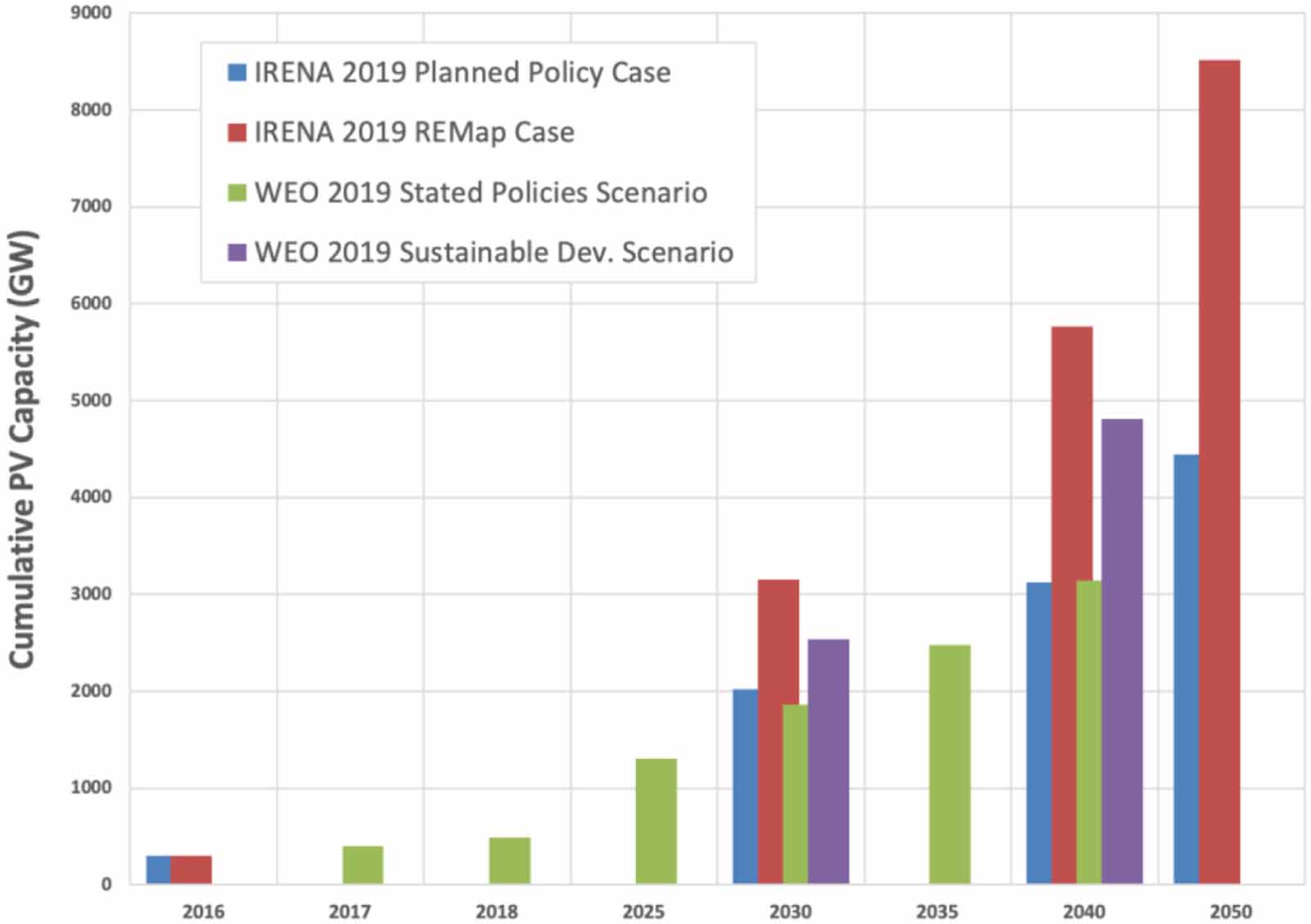
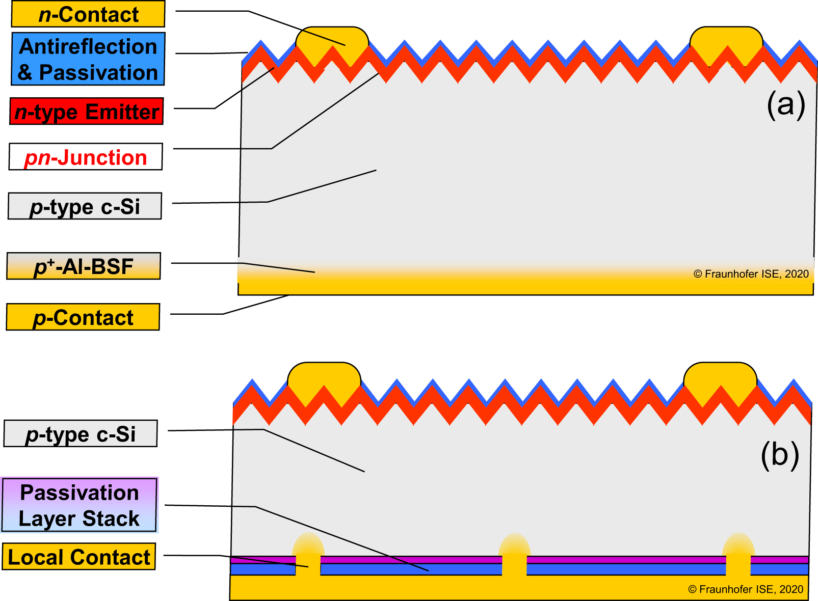
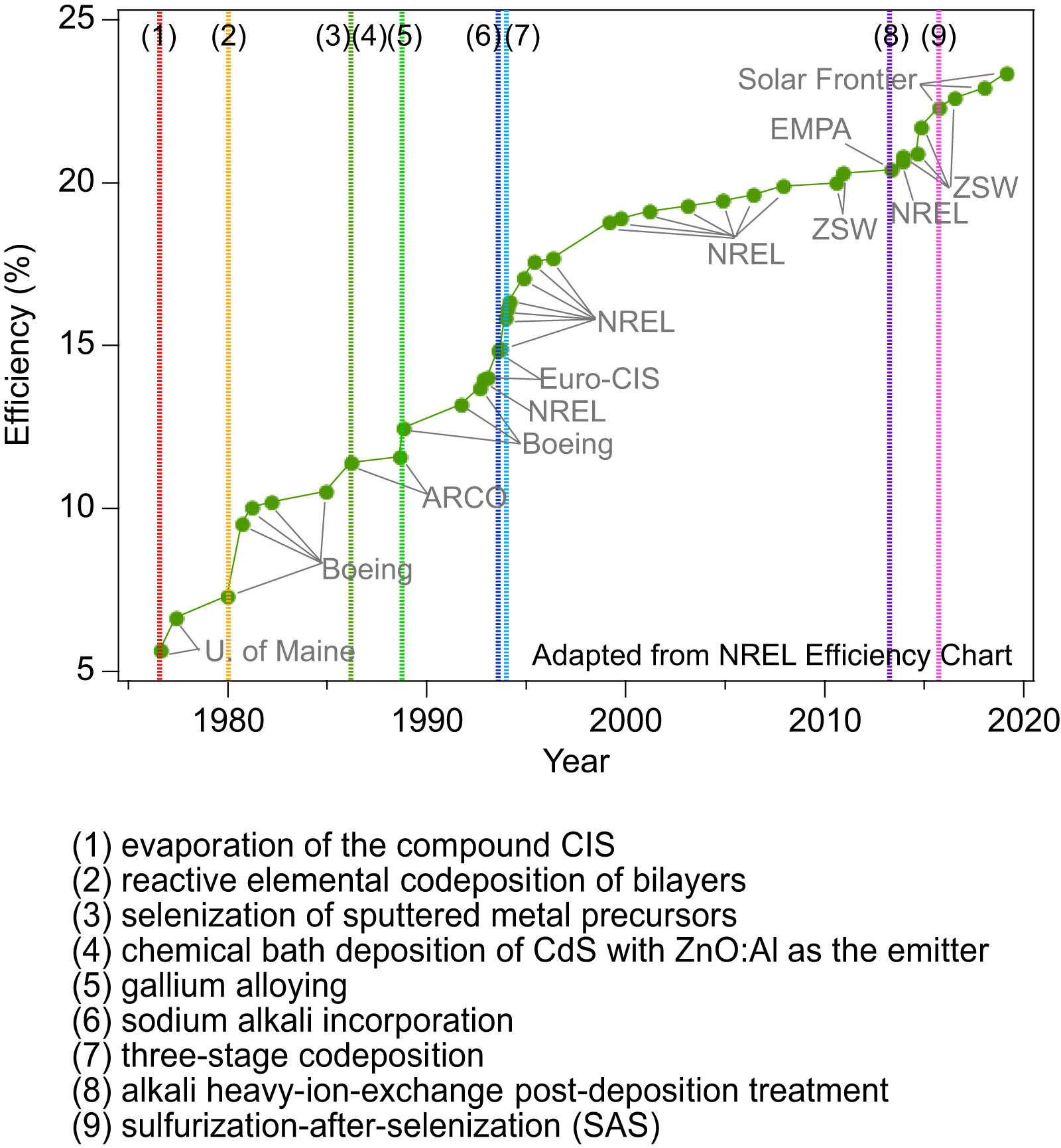
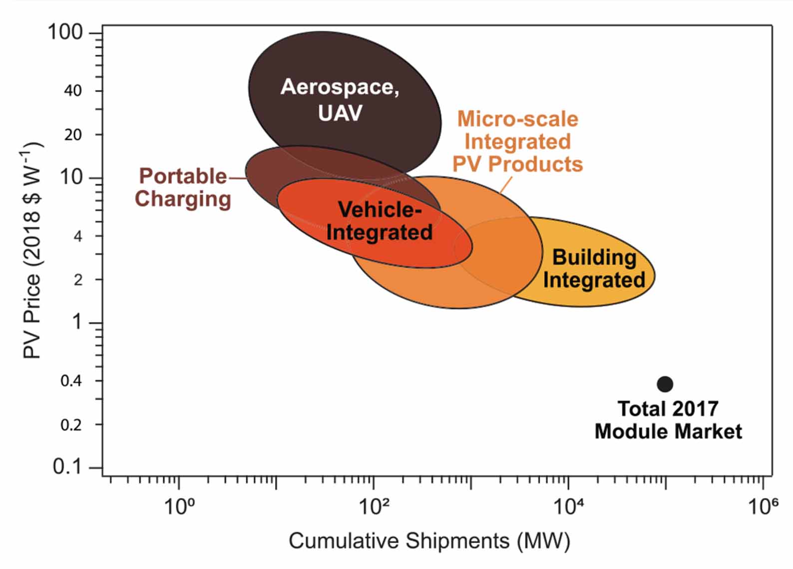
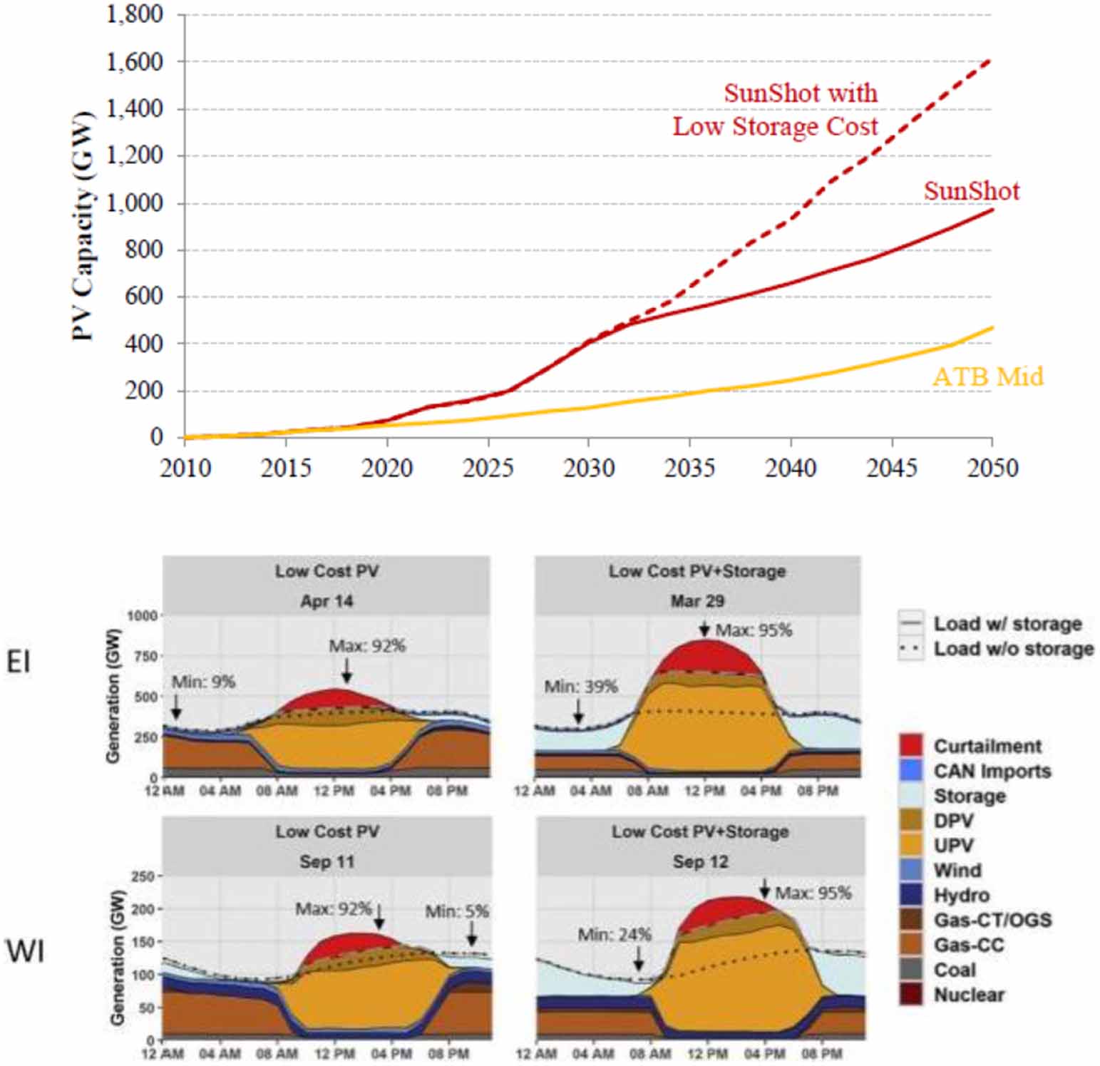
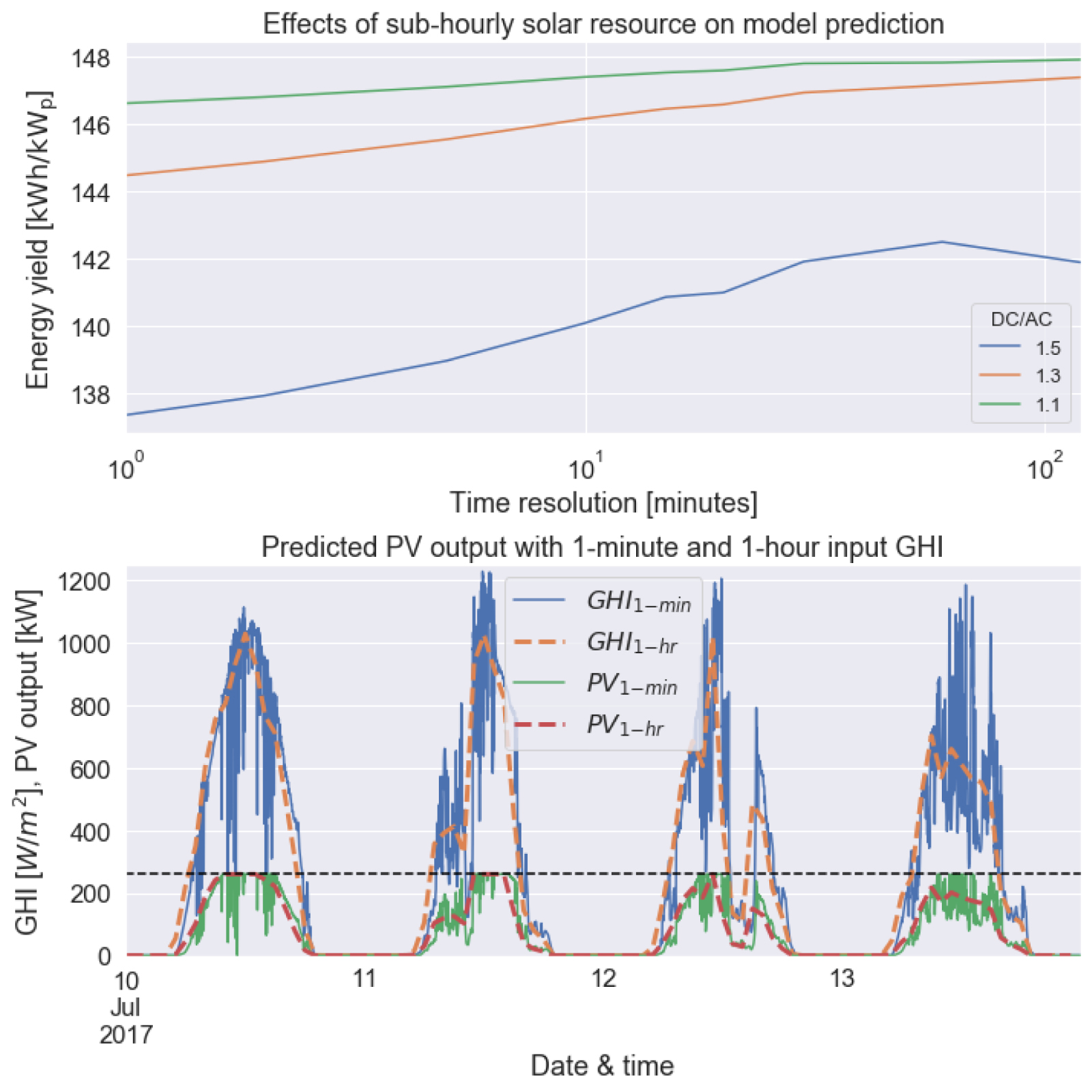
Figure 21. (a) Spatial ranges for different characterization methods, where blue represents primarily imaging techniques, green represents primarily analytical methods, and red represents combined imaging and analytical methods; (b) example of scanning transmission electron microscopy (STEM)/electron energy loss spectroscopy (EELS); (c) example of atom probe tomography (ATP); (d) example of electron backscatter diffraction (EBSD); (e) summary of module-scale imaging methods Reproduced from [144] CC BY 4.0. .
Download figure:
Standard image High-resolution image
12.3. Advances in science and technology to meet challenges
12.3.1. Multiscale characterization for cell and module development.
Combining field investigations, measurements of cored module pieces, and controlled studies on lab materials is necessary to understand the impacts of defects and process variations on long-term outdoor PV performance. To this end, it is particularly important to advance quantitative methods for distinguishing local versus global effects of interfaces and defects on I–V metrics. When defects at the module level are found, relevant characterization depends on cleaner and more reliable extraction of materials and interfaces for microscopic analysis. This necessitates improved coring techniques (e.g. mechanical drilling, waterjet, laser cold ablation, chemical treatment). Additional sample preparation such as mechanical polishing or focused-ion-beam milling may introduce impurities or microstructural changes, so advances in preparation methods (particularly for cross-sectional analysis) are needed. Beyond post-mortem analysis, verifying the applicability of accelerated stressing methods is needed to advance toward predictive approaches. In general, multi-method characterization can be expedited by increasing the user accessibility and throughput of specialized equipment, which will allow more inclusive characterization of a broader sample range.
12.3.2. Microscopic structural and chemical characterization.
The spatial resolution for structural characterization is one area that may not have a pressing need for further advances. However, greater sensitivity to atomic composition at high spatial resolution, especially for light elements, would help to make progress in understanding the effects of PV processing, contamination, and material degradation mechanisms. In addition to improving methods for direct detection of atomic signatures (e.g. SIMS, EDS, XPS, etc), in some cases it may be beneficial to explore the avenue of improving detectivity of defects with chemical treatments of the sample. While some methods do achieve high spatial resolution paired with high sensitivity to chemical composition (such as atom probe tomography, APT) [145], further development would be beneficial for making these methods more accessible for a wider range of users.
12.3.3. Electro-optical characterization.
Electro-optical characterization has great potential for non-destructive characterization of defects and recombination mechanisms occurring at the front/back surfaces, interfaces, or bulk regions of the materials and device structures. Significant progress is being made in distinguishing between processes occurring in these different sample regions via methods such as wavelength dependence, two-photon absorption, time-correlated techniques, and frequency-modulated lock-in characterization. Further development would be beneficial to target the characterization of specific sample layers, defect states, and micro/nano-structural features in a non-destructive way, especially at the level of encapsulated devices.
12.3.4. Outdoor characterization.
With growing PV field deployment, outdoor characterization methods are increasingly necessary to discover early signs of module degradation while preventing shut-down of operations. Thermal or luminescence imaging using drones and fly-over imaging are promising for statistical analysis of large systems. Other outdoor-compatible methods have been proposed, such as lock-in based sun-excitation photoluminescence imaging [146], UV-fluorescence of the encapsulant [146], pseudo-EQE measurements based on 'contactless' electroluminescence, and portable versions of FTIR, XPS, and reflectance.
12.4. Concluding remarks
The promising environmental and political benefits from implementing renewable energy has driven PV research for many years, and recently PV electricity is also becoming the economic choice for utilities providers. This makes it an exciting time to expand PV characterization efforts and build comprehensive understanding of PV performance and reliability from modules to atoms. Multi-scale characterization drives deeper understanding and targeted improvement of PV systems, where the use of complementary methods is essential to identify performance implications arising from specific device layers, components, defects, interfaces, additives, and so on. For further elucidating structure-function relationships between micro/nanoscale composition and semiconductor performance, additional improvements in chemical sensitivity paired with high spatial resolution would be beneficial to the community. Enabling more facile access of these characterization capabilities to a wider range of non-specialists is also critical for achieving broad understanding through greater statistics. In addition, continued development of non-traditional and outdoor-compatible instrumentation is essential for decreasing the cost of PV electricity while filling the needs of additional users through varied materials and technologies.
Acknowledgments
This work was authored in part by the National Renewable Energy Laboratory, operated by Alliance for Sustainable Energy, LLC, for the US Department of Energy (DOE) under Contract No. DE-AC36-08GO28308. Funding provided by the US Department of Energy Office of Energy Efficiency and Renewable Energy Solar Energy Technologies Office. The views expressed in the article do not necessarily represent the views of the DOE or the US Government. The US Government retains and the publisher, by accepting the article for publication, acknowledges that the US Government retains a nonexclusive, paid-up, irrevocable, worldwide license to publish or reproduce the published form of this work, or allow others to do so, for US Government purposes.