

Abstract
Crystalline silicon (c-Si) solar cells play an important role in the photovoltaic (PV) industry and make PV electricity begin to realize grid parity. Nevertheless, conventional c-Si solar cells are sensitive to angle of incidence (AOI) and have less power conversion efficiency (η) under oblique AOI, which influences the maximization of daily/yearly power output as the sun moves with time. Although the use of sun-tracking systems is an effective way to solve this problem, it is costly. As regards increasing the daily/yearly power output with low cost, quasi-omnidirectional c-Si solar cells are good candidates and have attracted considerable interest. The η of these solar cells is insensitive to AOI within a large range (for example, <60°) due to their quasi-omnidirectional antireflection ability. In this article, we will review different antireflection mechanisms and show how to realize quasi-omnidirectional antireflection in c-Si solar cells by specific structures, especially Si nanostructures due to their superior ability in manipulating light. We will see that quasi-omnidirectional c-Si solar cells can be realized by various Si nanostructures, but most of them suffer from lower η than conventional c-Si solar cells because of much more severe carrier recombination. Therefore, we will also present an overview of countermeasures and progress in mitigating electrical loss of quasi-omnidirectional c-Si solar cells. Finally, we will demonstrate high-performance quasi-omnidirectional c-Si, ultrathin c-Si and multicrystalline silicon solar cells realized by Si nanostructures with low aspect ratios and their advantages compared to their conventional c-Si counterparts.
Export citation and abstract BibTeX RIS
Corrections were made on 17 09 2020. Figure quality was improved.
1. Introduction
Solar cells that convert sunlight into electricity by the photovoltaic (PV) effect are playing increasingly important roles in solar energy. Compared to conventional electricity gneration by burning fossil fuels, solar cells are an environmentally friendly method and thus PV cells provide green electricity. Moreover, unlike fossil fuels, solar energy is sustainable. Thanks to a great improvement of power conversion efficiency (η) and reduction in cost, the amount of PV installations is increasing rapidly. In 2016, 76 GWp had been installed globally. Installation capacity was increased to 100 GWp in 2018 and the cumulative capacity reached at least 505 GWp [1]. New installation capacity further increased to ∼115 GWp in 2019 [2]. Such high installation capacity was mainly contributed by crystalline silicon (c-Si) solar cell modules. They account for about 95% of the PV market and are the most important PV technology in the industry at present [3]. We believe that the c-Si solar cells will continue to be the mainstream of the PV market for the next 10 or more years. This is because, compared to other solar cells, c-Si solar cells have obvious advantages such as high efficiency, low cost, non-toxicity and good stability. The η of c-Si solar cells in mass production is between 20% and 24%, and the record value in labs has reached 26.6% [4]. The module cost is less than %0.25 Wp−1. It is reported that the degradation rate of c-Si solar cell modules can be as low as 0.4%/year, which allows them to work reliably for 25 years [5, 6]. Generally, even after this period, their η can still maintain higher than 80% of its initial value. All these factors contribute to the relatively low levelized cost of electricity (LCOE) and approach PV grid parity. In some sunny places, the lowest bid price for a large-scale PV plant is already lower than the conventional electricity price. For example, the prices were 1.97 cents kWh−1 in Mexico (2017), 1.79 cents kWh−1 in Saudi Arabia (2017), 1.69 cents kWh−1 in Brazil (2019) and 1.35 cents kWh−1 in the United Arab Emirates (2020) [7–10].
LCOE will further decrease by improving the electricity generation ability of PV systems in a day/year. One of the methods to realize this goal is harvesting as many photons as possible. In conventional c-Si solar cells, the Si micropyramid texture is effective in suppressing reflection and thus is beneficial for harvesting photons [11]. However, its antireflection ability depends on the angle of incidence (AOI) [12, 13]. Surface reflectance increases with AOI, leading to a loss of incident photons that are potentially absorbed in c-Si wafers to generate electricity. As is known, the sun moves from east to west within a day, and moves between the northern hemisphere and the southern hemisphere in a year. These result in the change of AOI for PV modules mounted with a fixed angle and hence suggests the loss of electric energy production, which is common for PV plants. Sun-tracking systems are highly effective to address this problem. For example, a single axis tracker generally moves the PV panels on a single path from east to west, while two axis tackers allow PV panels to orientate towards any direction of the celestial sphere [14, 15]. As such, solar radiation collection is maximized. However, using a sun-tracking system leads to the increase of both purchase cost of PV systems and the maintenance of moving parts. Moreover, the distance between each system should be bigger than that between fixed systems, which indicates increased cost for land together with for cabling and communications [15]. It also should be noted that in some circumstances, it is hard to apply sun-tracking systems, for example in rooftop PV power stations.
Another effective method to reduce photon loss is developing quasi-omnidirectional c-Si solar cells, of which surface reflectance is independent of AOI over broad range. Through such a method, no additional installation and cost are added in PV systems, so it is considerably attractive. Applying nanostructure arrays is promising to realize quasi-omnidirectional solar cells [16–18]. Especially, it was reported that various Si nanostructure arrays have an excellent antireflection property over a broad wavelength and AOI [19–23]. Nevertheless, employing them on c-Si solar cells often results in worse η when compared to their conventional counterparts because of the degradation of electrical performances [24]. Optimizing Si nanostructures and adopting appropriate solar cell designs are required to achieve quasi-omnidirectional c-Si solar cells with high performance and realizing higher daily/yearly electric energy output than their conventional counterparts. To the best of our knowledge, this is the first review focusing on quasi-omnidirectional solar cells. It starts with briefly discussing various antireflection mechanisms that are often used in c-Si solar cells and pointing out the ones that achieve quasi-omnidirectional antireflection. Also, we present the methods used to obtain excellent quasi-omnidirectional antireflection, mainly based on Si nanostructures. Then we summarize the problems of quasi-omnidirectional c-Si solar cells realized with Si nanostructures and discuss the solutions to achieve high performance. Finally, the recent progress of quasi-omnidirectional c-Si solar cells is reviewed, focusing on the realization via Si nanostructures with low surface enhancement.
2. Realizing quasi-omnidirectional antireflection
2.1. Antireflection mechanisms
As shown in figure 1(a), when light travels from air to c-Si, Fresnel reflection occurs due to the change of refractive index, which results in a loss of incident photons and thus reduces the generated photocarriers. Generally, the reflectance at the air–c-Si interface can reach as high as 30%–40% [20, 25]. To reduce the reflectance, a thin film is usually coated on the c-Si surface. Figure 1(b) shows that reflections occur at the interface of air–thin film and the interface of thin film–c-Si, which result in an interference effect. If AOI = 0°,  and the relationship between a film thickness (dc) and a certain wavelength (λ0) satisfies
  , where nair, ns and nc represent refractive index of air, c-Si and the coating film, respectively, then reflectance near zero can be achieved at the λ0 due to the destructive interference effect, demonstrating an excellent antireflection effect near the λ0. However, such an antireflection effect depends on AOI and wavelength (λ) due to the phase difference between the incident and reflected waves [26]. Namely, for the given dc, if the AOI deviates from 0° or λ deviates from λ0, reflectance will increase. Hence, this antireflection mechanism is not an ideal choice for c-Si solar cells that work over broad AOI and λ.

Figure 1. Schematic diagrams of the interactions between light and c-Si wafers with different surface structures, which exhibit different antireflection mechanisms. (a) When light encounters a planar c-Si surface, Fresnel reflection occurs. (b) c-Si surface coated with a thin film, interference effect occurs. (c) c-Si surface with microstructure textures, multiple reflection and refraction happen. (d) Effective refractive index effect in Si nanostructures. (e) Light scattering effect between Si nanostructures. (f) Optical resonant effect in Si nanostructures. The red patterns represent electric field distribution of the optical resonances.
Download figure:
Standard image High-resolution imageSurface texturization is also a common method used to reduce surface reflectance, whose antireflection effect is independent of λ. In c-Si solar cells, Si micropyramids are generally adopted as surface textures, which are formed by anisotropic etching of c-Si wafers in alkaline solutions [27]. As presented in figure 1(c), through multiple reflections and refractions between Si micropyramids, the reflection that escapes c-Si wafers is greatly decreased and more photons are absorbed by c-Si wafers. Although Si mircropyramid textures are effective to reduce reflectance in c-Si solar cells, they cannot be formed in multicrystalline silicon (mc-Si) solar cells because the crystal orientations on the surface are different. Instead, Si microbowls or micropits are formed as the surface texture by isotropically etching of Si in acid solution [28]. It seems that whether the microtextures have a quasi-omnidirectional antireflection property or not depends on the shape of the microstructures. For example, the reflectance of a Si micropyramid-textured surface increases with AOI [12, 13], but Si microbowl-, micropit- or V-groove-textured surfaces exhibit a quasi-omnidirectional antireflection effect [29, 30].
The characteristic scale of the structure discussed above is muh larger than the wavelength of the photons that can be absorbed in c-Si solar cells (i.e. 300–1180 nm). Thus, geometry optics well explain the antireflection effect. Nevertheless, if the structures are much smaller than the wavelength (i.e. only several nanometers or several tens of nanometers), which are often called 'moth's eye' structures, light will not see the specific shape of the nanostructure and propagate through the structures as if they have a gradient refractive index, as schematically shown in figure 1(d). In this case, the effective medium theory is widely adopted. The effective refractive index of the nanostructures gradually changes from air to c-Si substrate, but the shape of the change depends on the morphology of the nanostructure arrays [31–33]. Note that such nanostructures with appropriate shape and height are highly effective in suppressing reflectance omnidirectionally since there is no interface.
If the characteristic scale of the surface texture is similar to wavelength, Mie scattering occurs between nanostructure arrays and forward scattering intensity is much larger than reverse scattering intensity, contributing to an antireflection effect, as shown in figure 1(e) [34]. In addition, scattering increases the optical length and thus increases light absorption in c-Si absorbers, which is also beneficial for the antireflection effect. In addition, nanostructures with this characteristic scale can also act as nanocavities. Light is strongly coupled into the nanostructures, forming optical resonances (also often called Mie resonance), and these optical resonances can extend into the underling c-Si substrate, as shown in figure 1(f) [35, 36]. The antireflection effect due to the optical resonance is quasi-omnidirectional. It should be noted that all the above antireflection mechanisms do not exclude each other in a specific antireflection structure. In fact, they often coexist and jointly contribute to an excellent quasi-omnidirectional antireflection effect in c-Si solar cells.
2.2. Quasi-omnidirectional antireflection performance
As discussed above, 'gradient refractive index' effect, light scattering effect and Mie resonance effect, which are realized by nanostructure arrays, play important roles in realizing quasi-omnidirectional antireflection. Considerable efforts have been devoted to investigating the outstanding antireflection effect of various nanostructures, aiming at improving light absorption of c-Si solar cells over broad AOI and λ. Lin et al employed ZnO nanorod arrays to form an effective refractive index with a gradient profile to realize excellent quasi-omnidirectional antireflection over broadband range [37]. Polydimethylsiloxane nanocone arrays were also used as quasi-omnidirectional antireflection film because of their smooth change of effective refractive index [38]. In addition, polystyrene nanospheres have been demonstrated to have broadband and quasi-omnidirectional light-harvesting abilities due to their strong forward scattering [34]. Generally speaking, the higher dielectric constant of nanostructures, the stronger the interaction between light and nanostructures, and thus a stronger effect in manipulating light. Therefore, Si nanostructures are highly attractive in c-Si solar cells to realize quasi-omnidirectional antireflection owing to their high dielectric constant.
Lin et al developed a controllable anisotropic wet-etching method to fabricate various Si nanostructures including nanopillars, nanorods, inverted nanopencils and nanocones, as shown in figures2(a1)–(a4), followed by a systematic study of their light management ability [23, 39]. It was found that the antireflection properties of the Si nanostructure arrays are predominantly decided by geometrical factors. Figures2(b1)–(b4) shows that all of the Si nanostructures can induce strong optical resonance inside the nanostructures, thus having lower reflectance than the planar surface (see figure 2(c)). However, inverted nanopencils more efficiently couple light into optical modes in the pencil base, resulting in the lowest reflectance over a broad wavelength range from 400 to 1000 nm. In addition, all the Si nanostructure arrays have quasi-omnidirectional antireflection over AOI of 0–60°, but inverted nanopencils keep the best antireflection ability over the broad AOI, which makes c-Si wafers with inverted nanopencils have highest absorption over the broad AOI, as shown in figure 2(d). Wang et al argued that Si nanocone arrays have excellent broadband antireflection because the Mie resonance wavelength in Si nanocones can be continuously tuned as the diameters of the cross sections increase from the top to the bottom [36]. Indeed, it is proved that the Mie resonance wavelength shifts approximately linearly with the diameter of Si nanostructures [40].

Figure 2. Schematic diagrams of (a1) Si nanopillars, (a2) Si nanorods, (a3) inverted Si nanopencils and (a4) Si nanocones. (b1)–(b4) are their corresponding electric filed intensity contours obtained by FDTD simulations. (c) Reflectance of Si planar surface and various Si nanostructured surface as a function of wavelength. (d) Absorption of c-Si with different surface conditions as a function of AOI. (e) Cross-sectional scanning electron microscope (SEM) image of Si nanowires. (f) Experimental and calculated reflectance of polished Si and Si nanowires versus AOI with polarized light (TE or TM). (a)–(d) Reprinted with permission from [23]. Copyright (2014), American Chemical Society. (e), (f) Reproduced from [25]. © IOP Publishing Ltd. All rights reserved.
Download figure:
Standard image High-resolution imageIn addition, there has been great effort devoted to fabricating Si nanowires or nanopores on c-Si wafers. Such Si nanostructures generally have a characteristic scale of only several tens of nanometers. As stated in section2.1, the antireflection effect in such nanostructures is often explained by effective medium theory, and good antireflection properties over broad AOI can be achieved by optimizing the effective refractive index profile [41]. Our group found that the reflectance of Si nanowire-textured c-Si wafers decreases with increasing the length of Si nanowires [25]. As shown in figure 2(e), on the one hand, an individual Si nanowire appears to be a tapered cylinder; on the other hand, Si nanowire arrays can be treated as bundled arrays. These two characteristics make Si nanowires arrays serve as a medium with a continuous gradient refractive index to reduce a mismatch of refractive indexes between air and c-Si substrate. The longer the Si nanowire arrays, the smoother the gradient buffer layers and hence the lower the reflectance. Figure 2(f) shows that near 0 reflectance over AOI of 0–60° is realized at an incident wavelength of 514.5 nm by using Si nanowires with a length of about 800 nm, demonstrating the excellent quasi-omnidirectional antireflection. Moreover, the antireflection ability is independent of polarization of incident light. These antireflection performances are well explained by effective medium theory and can be calculated by rigorous coupled-wave analysis [25]. In figure 2(f), the reflectance of s-(TE) and p-polarized (TM) light have a contrary trend versus AOI for polished Si wafers. This explains why a planar Si surface has almost the same reflectance over broad AOI (embodied by the same absorption as shown in figure 2(d)), but the reflectance is much higher than that of Si nanowires.
Si nanostructures with low surface area enhancement are attracting more and more interest as surface antireflection structures [42–44]. Pyramid-shaped, inverted pyramid and pitted surface structures generally have surface enhancement of only 1.7–2.0, as shown in figure 3(a). Low surface enhancement is beneficial for obtaining low surface carrier recombination, which will be discussed in detail in section3. Our group has deeply studied the antireflection properties of these surface structures over broad AOI [29, 45, 46]. To better illustrate the antireflection performance, here we show the simulated reflectance of Si micropyramids, inverted Si micropyramids, Si micropits and their nano-counterparts as a function of AOI in figures3(b)–(d). The reflectance of Si micropyramids, which are the standard antireflection structures in c-Si solar cells, increases linearly with AOI, agreeing well with the reported results [12, 47]. Nevertheless, the reflectance of Si nanopyramids only increases slightly within an AOI of 0–50°, presenting a quasi-omnidirectional antireflection ability. Beyond this range, it increases sharply. The reflectance of inverted Si micropyramids and inverted nanopyramids have similar behavior to their upright counterparts. The quasi-omnidirectional antireflection of upright Si nanopyramids or inverted nanopyramids is attributed to the effective couple of incident light into the optical resonance modes over the AOI of 0–50°, as illustrated in figure 3(e) [45, 46]. Besides size, the shape of the texturing structure also affects the dependence of antireflection performance on AOI. Unlike pyramidal structures, figure 3(d) shows that both micropits and nanopits have quasi-omnidirectional antireflection ability even though nanopits have much lower reflectance.
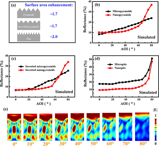
Figure 3. (a) Schematic illustration of Si pyramid-, inverted pyramid- and pitted-textured surfaces with their corresponding surface enhancement. Reflectance of (b) Si nanopyramids, (c) inverted nanopyramids, (d) nanopits and their corresponding microstructure counterparts as a function of AOI. (e) Electric field intensity mapping of inverted Si nanopyramid-textured c-Si varying with AOI. (e) Reproduced from [46]. Copyright 2017, IOP Publishing Ltd.
Download figure:
Standard image High-resolution imageIntegrating Si nanostructures with Si microstructures, forming a so-called 'multi-scale texture' or 'hierarchical structure', is expected to have an antireflection effect from both Si nanostructures and microstructures [49–52]. Figure 4(a) shows an example of the hierarchical structures. Si nanowires stand on Si micropyramids. Figure 4(b) demonstrates that the hierarchical structure and Si nanowires outperform Si micropyramids in terms of antireflection ability versus AOI [12, 53–55]. Moreover, the hierarchical structure has a superior quasi-omnidirectional antireflection effect than Si nanowires. Based on a hierarchical structure, Pei et al further investigated the influence of the orientation of Si nanowires on the antireflection effect [19]. Si micropyramids with <111> oriented Si nanowires, namely Si nanowires perpendicular to pyramidal surface, have a better antireflection effect than Si micropyramids with <100> oriented Si nanowires over the AOI from 0 to 75°, suggesting a superior quasi-omnidirectional antireflection property.

Figure 4. (a) A hierarchical structure containing Si micropyramids and Si nanowires. (b) Average reflectance normalized to polished Si for different surface textures varying with AOI. (c) Cross-sectional SEM image of Si nanocones coated with SiNx film. (d) Absorptance of Si nanopillars coated with TiO2/SiO2 double-layer films varying with AOI and wavelength. (b) Reprinted from [12], Copyright (2016), with permission from Elsevier. (c) Reprinted from [21], Copyright (2014), with permission from Elsevier. (d) Reprinted by permission from Springer Nature Customer Service Centre GmbH: Applied Physics B: Lasers and Optics [48] (2017).
Download figure:
Standard image High-resolution imageCoating Si nanostructures with thin films is also commonly utilized to realize outstanding antireflection performance due to combined antireflection effects from optical resonances and destructive interference effects [56]. Figure 4(c) shows a cross-sectional scanning electron microscope (SEM) image of Si nanocones coated with SiNx film. Such composite structure greatly reduces surface reflectance over the wavelength of 290–2000 nm at any AOI up to 60° [21]. Similarly, coating Si nanopillars with SiNx results in excellent quasi-omnidirectional antireflection over AOI of 0–60°, much better than flat Si and flat Si with SiNx. The good antireflection is explicitly explained by the combined effect of the strongly coupled Mie resonances and the interference antireflection effect [35]. Zheng et al further investigated the quasi-omnidirectional antireflection of Si nanopillars coated with TiO2/SiO2 double-layer films [48]. Such a composite structure contributes to high optical absorption in c-Si substrate, higher than 95.8% over the AOI from 0 to 60°, as shown in figure 4(d). Our group found that both upright Si nanopyramids and inverted Si nanopyramids coated with SiNx also have a much better quasi-omnidirectional antireflection effect compared to the ones without SiNx coating (average reflectance decreases by ∼8% absolutely) [45, 46].
3. Difficulties and countermeasures for quasi-omnidirectional c-Si solar cells
3.1. Quasi-omnidirectional solar cells with large surface enhancement
Due to their excellent antireflection effect, as presented above, Si nanostructures have been widely tried as surface textures in c-Si solar cells. In the early stage, interest mainly focused on Si nanostructures with a high aspect ratio because of their better antireflection effect [57–59]. Figures 5(a) and (b) are the top-view and side-view SEM images of needle-like Si nanostructures. The average height of the nanostructures is about 2 μm. This unique structure leads to an ultralow average reflectance, only 1.79%, and makes the c-Si wafers have a black appearance, thus termed 'black silicon'. Figure 5(c) shows that black silicon has much lower reflectance than micropyramid-textured silicon and polished silicon over a broad wavelength, presenting overwhelming advantages in the optical performance. However, such an optical advantage does not lead to better solar cell performance. On the contrary, black silicon solar cells have much lower external quantum efficiency (EQE) over a broad wavelength compared to the reference solar cells (micropyramid-textured), as shown in figure 5(d). As a result, their η is lower. It was found that the higher the nanostructures (no matter nanohillocks or nanowires), corresponding to larger surface enhancement, the better the antireflection effect, but the worse the EQE or internal quantum efficiency (IQE) [60, 61]. On mc-Si solar cells, Si nanostructures such as nanohillocks and nanopores also lead to worse EQE and current–voltage (J–V) performances than the conventional surface texture [61, 62]. The IQE spectra can be well fitted by PC1D simulations if assuming that the Si nanostructure layer acts as a low lifetime 'dead layer' [63]. The 'dead layer' is attributed to high Auger recombination and additional recombination at the numerous internal surfaces. The higher the Si nanostructures, the thicker the 'dead layer'. Hence, in spite of remarkable antireflection effect, photogenerated carriers cannot effectively contribute to the output current. As a result, although Si nanostructure-textured solar cells have quasi-omnidirectional short-circuit current density (JSC), its JSC may be lower than that of conventional solar cells at any AOI between 0 and 60°, which affects the attractiveness of Si nanostructures in c-Si solar cells [13].

Figure 5. (a) Top-view and (b) side-view SEM images of needle-like Si nanostructures. (c) Reflectance of c-Si wafers with different surface textures. (d) Comparison of EQE spectra of black silicon solar cells and reference solar cells. Reprinted from [59], Copyright (2011), with permission from Elsevier.
Download figure:
Standard image High-resolution image3.2. Electrical loss by carrier recombination
To gain an insight into the poor electrical performance of quasi-omnidirectional solar cells featuring Si nanostructures as surface texture, Oh et al have thoroughly investigated the effective carrier lifetime (τeff) and effective surface recombination velocity (  ) of c-Si wafers with passivated n+-p junctions as functions of sheet resistance (related to doping profile) and surface area enhancement ratio (AF/Aproj), wherein AF is the nanostructured surface area and Aproj is the projected area on planar surface [64]. Figure 6(a) shows that τeff strongly decreases with increasing surface area at any given sheet resistance despite the thermal SiO2 passivation layer. This suggests that Si nanostructures promote carrier recombination and the higher the Si nanostructures, i.e. the larger the surface area enhancement, the more severe the carrier recombination. As regards sheet resistance, its influence depends on the regions, as indicated by the color-coded regions in the figure. For any given Si nanostructures (or given surface area), the τeff increases with sheet resistance from ∼55 to ∼100 Ω □−1 (region I), and then stays almost unchanged for sheet resistance between 100 and 200 Ω □−1 (region II). Further increasing sheet resistance (region III), τeff decreases due to the weakening of the built-in electric field.
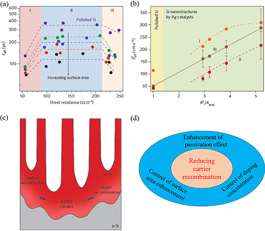
Figure 6. (a) Effective carrier lifetime (τeff) and (b) effective surface recombination velocity ( ) of polished and nanostructured silicon varying with sheet resistance and surface area enhancement ratio (AF/Aproj). (c) Schematic diagram of carrier recombination mechanisms in Si nanostructures. (d) Countermeasures for reducing carrier recombination in Si nanostructures. (a)–(c) Reprinted by permission from Springer Nature Customer Service Centre GmbH: Nature Nanotechnology [64] (2012).
Download figure:
Standard image High-resolution imageFigure 6(b) plots the relationship between  and AF/Aproj.
  is extracted from minority carrier lifetime measurement.
  , where
  is the local effective surface recombination velocity at and very near the actual front surface. Evidently,
  linearly increases with AF/Aproj in region III, suggesting that
  is constant and surface recombination is the exclusive recombination mechanism in the light doping region. Nevertheless, in region I (heavy doping region),
  severely deviates from linear dependence on AF/Aproj. Especially, when AF/Aproj is above 3.8,
  becomes nearly independent on surface area. This indicates that for heavily doped Si nanostructures, especially those with high aspect ratio, carrier recombination is not dominated by surface recombination, but by other recombination mechanisms. To explain this behavior, figure 6(c) schematically shows the carrier recombination process within an emitter with Si nanostructures that feature lateral sizes within 100 nm [64]. For a nanostructured wafer, the doping concentration is almost constant and close to the surface peak concentration throughout the entire Si nanostructures. As is known, for a heavily doped emitter, Auger recombination becomes highly important and strongly reduces τeff and increases
  . Hence, for heavily doped Si nanostructures, carriers are recombined within an emitter via Auger recombination rather than recombined on the surface through surface defects. As a result,
  increases with the volume of the heavily doped silicon rather than directly depending on surface area. For lightly doped Si nanostructures, Auger recombination is suppressed and
  primarily depends on surface recombination, relating to surface area. In the moderate doping region, namely region II,
  slightly deviates from linear dependence on AF/Aproj because both surface recombination and Auger recombination cannot be neglected.
3.3. Countermeasures to enhance the performance of quasi-omnidirectional solar cells
Now, it is evident that suppressing surface recombination and Auger recombination channels are the key factors to achieve high-performance quasi-omnidirectional solar cells featuring Si nanostructures as surface texture. Figure 6(d) illustrates the countermeasures to reduce carrier recombination, namely control of surface area enhancement, control of doping concentration and enhancement of passivation effect [24]. Firstly, the surface area enhancement should be controlled to reduce surface defects, thus reducing the surface recombination. To this end, multi-scale texture, optimization of Si nanostructure density and developing Si nanostructures with low surface area enhancement are the potential solutions. Note that these measures also often result in reduced emitter volume, thereby lowering Auger recombination. Multi-scale structures combine antireflection effects from both microstructures and nanostructures. In this case, even if the Si nanostructures are shorter, corresponding to lower surface area enhancement, an excellent antireflection effect is still retained while low carrier recombination could be achieved. Hence Si nanopores [49, 65–67], Si nanowires [51, 53, 54, 68, 69] or Si nanocones [70] have been widely fabricated on Si micropyramids, and Si nanoholes [62, 71], Si nanowires [72] and nanoscale Si pseudo-pyramids [29, 42, 73] have been fabricated on Si micropits with attempts to realize high-performance c-Si solar cells and mc-Si solar cells, respectively. Optimization of Si nanostructure density is another important approach to control surface area enhancement [56]. Jung et al demonstrated that, for a given light absorptance, Si nanowires with higher filling ratio require lower height [74]. Consequently, surface area enhancement decreases, which leads to better solar cell performances. For example, Si nanowires with a filling ratio of 38% and length of 1.2 μm have the same antireflection effect as the nanowires with the filling ratio of 12% and length of 6 μm, but their surface area enhancement is about 11% lower in absolute value, resulting in that the η increases from 6.62% to 9.65%. In addition to multi-scale texture and optimization of Si nanostructure density, developing Si nanostructures with low surface area enhancement is also highly promising to realize high-performance quasi-omnidirectional c-Si solar cells, which will be discussed in section4 in detail.
Secondly, emitter doping concentration should be carefully controlled since the entire Si nanostructure layers are facile to be heavily doped, leading to severe Auger recombination. Reducing doping concentration was demonstrated to be effective to decrease carrier recombination and thus improved blue spectral response of solar cells [64, 75, 76]. Nevertheless, too light doping will lead to high sheet resistance, and thereby influence fill factor. A trade-off between carrier recombination and resistance effect should be considered for optimizing emitter doping concentration. A heterojunction structure whose emitter is external to c-Si wafers could be a good solution to this dilemma. Thirdly, realization of an excellent passivation effect is another extremely significant countermeasure to suppress carrier recombination channels since most Si nanostructures have relatively high surface enhancement, indicating a high surface recombination center. Thermally grown SiO2 film [64, 69, 77], plasma-enhanced chemical vapor deposition grown SiNx:H [42, 71, 72] and atomic layer deposited (ALD) Al2O3 film [78] are the most popular passivation layers on Si nanostructures due to their outstanding chemical passivation and/or field-effect passivation. Chemical passivation is an effect to remove the dangling bonds on a c-Si surface such as by forming Si–O bonds in the case of SiO2 and Si–H bonds in the case of SiNx:H. Field-effect passivation involves repelling a certain type of charge carrier (either electrons or holes) away from the c-Si surface such as by negative fixed charges in Al2O3 and positive fixed charges in SiNx:H [24].
Svain et al showed a remarkable example to realize high-performance quasi-omnidirectional c-Si solar cells by successfully minimizing carrier recombination [79]. The solar cell structure is schematically shown in figure 7(a). The front side is textured by Si nanopillars with a typical height of ∼800 nm and width of 200 nm. This results in extremely low reflectance over 300 to 1000 nm, thus being called black silicon (abbreviated to b-Si in figure 7). They adopted interdigitated back contacts (IBCs) as the solar cell design, namely that junctions and contacts are placed at the back side of solar cells. With this design, there are at least two advantages: (i) no grids shadow on the front side; (ii) no doping requirement in Si nanostructures, avoiding Auger recombination. Moreover, the Si nanostructures are well passivated by ALD Al2O3. Figure 7(b) shows a surface recombination velocity of only ∼20 cm s−1 on the nanostructured sample. Although it is still a little higher than that (∼3 cm s−1) of the reference sample with random Si micropyramids as surface textures, it is good enough to demonstrate the excellent passivation effect on nanostructured samples and is in the acceptable range for high-performance IBC solar cells. Consequently, an impressive η (22.1%) has been achieved, as presented in figure 7(c). The JSC reaches 42.2 mA cm−2 and open-circuit voltage (VOC) is 665 mV, which prove the superior front-surface passivation in the nanostructured solar cells. These values are comparable to those of reference solar cells. Figure 7(d) demonstrates the relative change in JSC with respect to normal illumination for several AOI. As regards the nanostructured cell, changes of JSC are less than 1% for AOI below 60°, exhibiting a quasi-omnidirectional property in cell level. Nevertheless, for the reference counterpart, changes of JSC are up to nearly 4% in this range. Considering the fact that the sun moves with time and thus AOI changes, the nanostructured solar cells will have a higher electric energy yield throughout the day/year.

Figure 7. (a) Structure of IBC solar cells with Si nanopillars on the front side, which is passivated by ALD Al2O3. Due to the nanostructured surface, such Si wafers are often called black silicon (b-Si). (b) Comparison of surface recombination velocity between b-Si and reference sample with random micropyramids. (c) Current–voltage (J–V) and power–voltage (P–V) characteristics of the optimal b-Si solar cell. (d) Relative JSC, with respect to JSC at normal incidence, for different AOI for both b-Si and reference solar cells. (b)–(d) Reprinted by permission from Springer Nature Customer Service Centre GmbH: Nature Nanotechnology [79]. (2015).
Download figure:
Standard image High-resolution image4. Quasi-omnidirectional solar cells realized by Si nanostructures with low surface enhancement
4.1. Fabrication of Si nanostructures with low aspect ratios
The above example is impressive, but the IBC solar cell structure, which is adopted to mitigate Auger recombination and remove grid shadows, needs a sophisticated fabrication process. Moreover, there are concerns that Si nanostructures like Si nanopillars have a relatively high aspect ratio and collapse easily. Concerning these matters, Si nanostructures such as Si nanopyramids and nanopits with a bowl-like shape are robust and they have low surface area enhancement, at least similar to conventional counterparts, so they are easier to get well passivated. In addition, these nanostructures combining with appropriate thin films also have a highly effective antireflection effect, as mentioned in section2. Due to these advantages, there are numerous reports about fabricating upright or inverted Si nanopyramids. The nanoimprint lithography method is one of the popular methods used to fabricate Si nanopyramids (including upright or inverted) [80–83]. Firstly, a dielectric layer (SiO2 or SiNx) and an imprint resist are grown on the c-Si surface as an etching mask, followed by mold imprinting, UV curing and plasma treatment, and then reactive ion etching and HF solution are used to remove the residual imprint resist and the dielectric layers to define the opening window of Si surface. In the following, the samples receive alkaline etching, and finally they receive HF etching again, thus forming the Si nanopyramidal surface. Besides nanoimprint lithography, the interference lithography method is also employed to define the etching patterns and thus produce Si nanopyramids [84–86]. SiO2 and photoresist layers are deposited on the c-Si surface first, and then interference lithography is used to define etching patterns, followed by reactive ion etching, HF etching, alkaline etching to form Si nanopyramids and, finally, the samples go through HF etching again to remove the oxide layers. Nanosphere lithography technology can be also utilized to define the etching patterns, and the steps of the deposition of mask, plasma etching and removal of mask are needed [87].
The above methods to fabricate Si nanopyramids are mainly based on lithography technology. The processes are rather complicated and expensive. Now, all-solution-processed methods to form Si nanopyramids will be presented in the following. The metal-assisted alkaline etching (MAAE) method was proposed to produce upright Si nanopyramids, as shown in figure 8(a) [45, 88]. C-Si wafers are immersed in AgNO3/HF solution to form a thin layer of Ag nanoparticles on the Si surface. Then the samples receive alkaline etching under solution temperature of 55 °C–75 °C, followed by the removal of Ag nanoparticles in HNO3 solution. With these three steps, Si nanopyramids with a clean surface are produced. As can be seen, the MAAE method does not require an etching pattern and thus
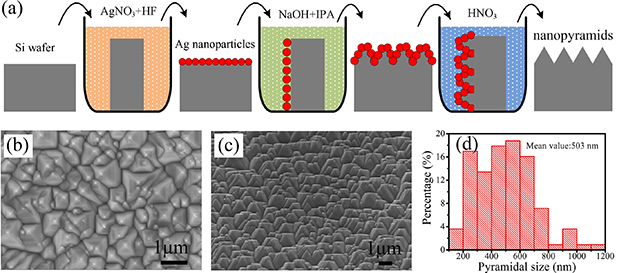
Figure 8. (a) Schematic diagram of the fabrication process of Si nanopyramids through the metal-assisted chemical etching method. (b) Top-view, (c) tilted-view SEM image, and (d) size distribution of Si nanopyramids. Reproduced from [45]. CC BY 4.0.
Download figure:
Standard image High-resolution imagedoes not involve lithography process or ion etching. It is simple and cost-effective. The typical top-view, 45°-tilted-view SEM images and the pyramidal size distribution of the Si nanopyramids are shown in figures 8(b)–(d). The Si nanopyramids are densely distributed no matter from top view or 45°-tilted view, exhibiting perfect surface textures. They have sizes from 100 to 1200 nm but concentrated in 200 to 800 nm with a mean value of 503 nm. Furthermore, compared to conventional Si micropyramids, Si nanopyramids have much smoother surfaces, which is beneficial for reducing surface recombination [45]. Besides upright Si nanopyramids, inverted Si nanopyramids can also be fabricated by an all-solution-processed method [46]. Firstly, c-Si wafers are immersed in AgNO3/HF solution to form a thin layer of Ag nanoparticles on the surface (Step 1), but then being different from MAAE method, the wafers are etched in H2O2/HF solution to result in a Si nanohole-textured surface (Step 2). These two steps are often called metal-assisted chemical etching (MACE) [89]. In the following, Ag nanoparticles are removed in HNO3 solution, and finally Si wafers receive alkaline etching to convert Si nanoholes into inverted Si nanopyramids (Step 3). Evidently, this method is also simple and does not involve the lithography process. Moreover, the sizes of the inverted Si nanopyramids can be well controlled by adjusting the etching time in Step 2 and Step 3. For example, increasing the etching time in these two steps, inverted Si nanopyramids become larger.
This method (MACE with post-alkaline etching) has also been applied to mc-Si solar cells and is effective to enhance their η [42, 73, 90]. Nevertheless, the etching process of c-Si in alkaline solution is anisotropic, which results in different Si nanostructures on different crystallographic planes and thus different appearance. As it is known, mc-Si wafers have different crystallographic planes on the surface, and considering aesthetics, solar cells should have a uniform visual appearance. Therefore, MACE with post-alkaline etching is an imperfect texturing option for mc-Si solar cells. Instead, MACE with post-acid etching could be a better approach since etching of Si in acid solution is isotropic [29]. The process is that Si wafers are immersed in AgNO3/HF/H2O2 solution to deposit Ag nanoparticles and form Si nanopores, followed by etching in HNO3/HF solution to produce Si nanopits and removing Ag nanoparticles in HNO3 solution. Figures 9(a–d) shows that the Si nanopits are bowl-like structures. They are uniformly distributed on the mc-Si surface in spite of different crystallographic planes. As a result, the mc-Si solar cells with post-acid etching treatment exhibit much better visual appearance and less noticeable grain boundaries compared to their counterparts with post-alkaline etching, as shown in figures9(e) and (f). Note that such bowl-like nanostructures can be also fabricated by MACE, followed by thermal oxidation and the removal of oxide layers in HF solution [44]. In the following, we will focus on the application of these Si nanostructures with low aspect ratio in quasi-omnidirectional solar cells.
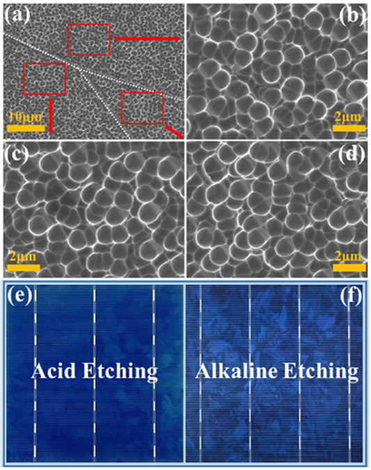
Figure 9. (a) SEM image of Si nanopits on different crystalline grains, wherein white dashed lines guide grain boundaries. (b)–(d) Zoomed-in SEM images of the red frame zones shown in (a). Digital photography of the mc-Si solar cells textured by MACE with (e) post-acid etching and (f) post-alkaline etching. Reprinted from [29], Copyright (2018), with permission from Elsevier.
Download figure:
Standard image High-resolution image4.2. Quasi-omnidirectional c-Si solar cells
From an optical aspect, Si nanopyramids result in a dramatic reduction of reflectance compared to the planar surface. Especially, when the Si nanopyramids are coated with SiNx or transparent conductive layers, reflectance is greatly reduced further, leading to an average reflectance of only about 3.6% [45]. From an electrical aspect, these Si nanopyramids have much lower surface enhancement than nanostructures such as nanopores and nanowires, which is beneficial for reducing carrier recombination. In fact, even if compared to conventional Si micropyramids, the Si nanopyramids fabricated by the MAAE method also have a little lower surface enhancement (the surface enhancement ratios for the Si nanopyramids and Si micropyramids are 1.48 and 1.62, respectively) due to lower base angles and smoother surfaces, hence resulting in lower surface recombination [45]. Through adopting intrinsic amorphous silicon film as a passivation layer, the VOC of the Si nanopyramid-textured solar cell reaches 729 mV, which is the highest value for the nanostructured solar cells. Its η reaches 20% on a large-size wafer (156 × 156 mm).
More importantly, the Si nanopyramid-textured solar cells exhibit an obviously quasi-omnidirectional antireflection property, as shown in figure 10. The Si nanopyramid -textured wafer looks black no matter from top view or tilted-angle view, whereas the conventional Si micropyramid-textured wafer looks black from top view and becomes shining from tilted-angle view. EQE spectra further demonstrates that the EQE of Si micropyramid-textured solar cells decreases with increasing AOI from 0 to 75°. However, the EQE spectra of Si nanopyramid textured solar cells are almost unchanged when AOI is in the range of 0–45°, which is similar to that of Si nanopillar-textured solar cells [79]. The quasi-omnidirectional EQE performance originates from the quasi-omnidirectional antireflection of Si nanostructures, as discussed in section2. Due to this quasi-omnidirectional property, the Si nanopyramid-textured solar cells (both homojunction and heterojunction structures) have higher output power (Pout) than their micropyramid-textured counterparts at most times of the day, taking Shanghai (latitude of 31°) as an example of installation location. Note that they have comparable η under standard measurement conditions, indicating under normal incidence. It was further demonstrated that the Si nanopyramid-textured solar cells have more electric energy production than their counterparts on four representative days in spring, summer, autumn and winter. Especially, the relative enhancement approaches 2.5% in winter. Therefore, the Si nanopyramid-textured solar cells will have higher electric energy production in a year than their conventional counterparts.
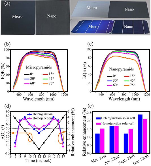
Figure 10. (a) Digital photographs of Si micropyramid-textured and nanopyramid-textured wafers taken under normal angle and tilted angle. Photos of the corresponding solar cells under tilted angle are also presented. EQE spectra of (b) Si micropyramid-textured and (c) nanopyramid-textured heterojunction solar cells varying with AOI. (d) AOI and relative enhancement ratio of the Pout of Si nanopyramid-textured solar cells compared to Si micropyramid-textured counterparts as a function of time on 23 September. Both homojunction and heterojunction structures are included. (e) Relative enhancement of energy output of the Si nanopyramid-textured solar cells (both homojunction and heterojunction structures) on 21 March, 22 June, 23 September and 22 December, as compared to Si micropyramid-textured cells. Reproduced from [45]. CC BY 4.0.
Download figure:
Standard image High-resolution imageSimilar results have been also demonstrated in inverted Si nanopyramid-textured c-Si solar cells [46]. By using a passivated emitter and rear cell design, the η reaches 20.5% on a large-size wafer (244.3 cm2). Moreover, inverted Si nanopyramid-textured c-Si solar cells have a lower reverse saturation current density than Si nanowires/micropyramids hierarchical solar cells [46, 91], suggesting lower carrier recombination velocity. As presented in figure 3(e), the incident light is similarly coupled into c-Si wafers by scattering and resonant effects when the AOI is within 60°, leading to quasi-omnidirectional antireflection. This antireflection effect is enhanced by coating inverted Si nanopyramids with SiNx films. As a result, inverted Si nanopyramid-textured solar cells have quasi-omnidirectional EQE. Namely, the EQE is insensitive to AOI when it is within 60°. Thus, it is expected that inverted Si nanopyramid-textured solar cells will have higher electric energy production than Si micropyramid-textured solar cells.
4.3. Quasi-omnidirectional ultrathin c-Si solar cells
Si nanopyramids have also been employed to fabricate quasi-omnidirectional ultrathin c-Si (thickness <50 μm) solar cells [92]. Since c-Si is an indirect bandgap material and has low absorption efficiency, when the thickness reduces to smaller than 50 μm, the light trapping effect becomes extremely significant. Si nanopyramids could help to obtain an excellent light trapping effect. By applying Si nanopyramids coated with SiNx film at the front side and Si nanopyramids coated with SiNx/Ag dual layers at the back side, the light absorption of ultrathin Si wafers becomes much higher than that of a planar wafer with similar configurations and approaches Lambertian absorption [88]. For an ultrathin c-Si wafer with a thickness of only 30 μm, the maximum JSC reaches 39.8 mA cm−2, which is calculated from the light absorption spectrum. Note that inverted Si nanopyramids have a similar advantage [46], but we will not discuss that here. Besides the light trapping effect, low surface recombination is another vital factor affecting the performance of ultrathin c-Si solar cells. Considering this, the Si nanopyramid texture is a better option than other nanotextures due to its lower surface enhancement. In addition to using Si nanopyramids as a surface texture, our group has further adopted an amorphous silicon/c-Si heterojunction concept as a solar cell design, which is known for its excellent passivation effect [92]. As a result, the surface recombination reduces to 1.83 cm s−1 and the implied VOC is 719 mV, successfully demonstrating the low carrier recombination of the Si nanopyramid-textured ultrathin solar cells.
Ultrathin c-Si solar cells have an issue that they are easy to break in the fabrication process. Concerning this, in the step of fabricating electrodes, direct copper metallization is a better option than screen printing, which is the standard metallization technique in the present PV industry. Direct copper metallization is realized by multi-wire technology [93]. The polymer-coated copper (C/Cu) wires are soldered directly on a transparent conductive oxide (TCO) layer of solar cells. The electric contact between C/Cu wires and TCO layers is realized through the outer conductive polymer coating films that contains adhesive agent to glue wires onto TCO layers. The multi-wire technology avoids high pressure during the metallization process, which reduces the risk of fragmentation. By applying the Si nanopyramid texture, the heterojunction solar cell design and direct copper metallization, an η of 15% has been demonstrated on a 37 μm thick c-Si wafer as a proof of concept [92]. In the ultrathin c-Si solar cells, quasi-omnidirectional EQE has also been proved. The EQE is insensitive to AOI when AOI is within 60°, but the EQE of the ultrathin c-Si solar cells with Si micropyramids obviously decreases with AOI. Consequently, the JSC of the ultrathin c-Si solar cells textured with Si nanopyramids is insensitive to AOI over broad AOI, presenting higher electric energy production ability than their Si micropyramid-textured counterparts.
4.4. Quasi-omnidirectional mc-Si solar cells
Diamond wire sawn (DWS) is gradually becoming the dominant slicing technique in PV Si wafers due to its advantages of higher productivity, higher precision in cutting thin wafers and lower material waste. Nevertheless, surface texturization in DWS mc-Si wafers is not as effective as in multiwire slurry sawn mc-Si wafers. Figure 11(a) shows the SEM image of the surface of a DWS mc-Si wafer textured by the conventional micro-texture (CM-T) method, namely etched in HNO3/HF solution. The surface is distributed with parallel grooves with different width (from nanometers to micrometers), which is an unsatisfactory texture due to high reflectance. Nevertheless, the MACE method with post-acid etching results in a totally different surface structure, as shown in figure 9. Bowl-like Si nanopits are densely distributed on the DWS mc-Si surface. Moreover, such a texture leads to much lower reflectance than the CM-T surface over a broad wavelength from 400 to 1100 nm [29]. After coating SiO2/SiNx stack layers, the antireflection effect is enhanced in the whole wavelength range for both the CM-T surface and the Si nanopit-textured surface, but the reflectance of the nanopit-textured surface remains much lower than that of the CM-T surface in the short wavelength region (<700 nm). Therefore, mc-Si solar cells with nanopits have much higher EQE at short wavelength than the ones with CM-T.

Figure 11. (a) SEM image of a conventional microtexture (CM-T) with cross-section view in the inset. EQE spectra of the (b) CM-T and (c) nanopit -textured mc-Si solar cells varying with AOI. (d) Comparison of their JSC varying with AOI. Reprinted from [29], Copyright (2018), with permission from Elsevier.
Download figure:
Standard image High-resolution image
Figures 11(b) and (c) show the EQE spectra varying with AOI. Both the CM-T and Si nanopit-textured mc-Si solar cells have quasi-omnidirectional EQE. Their EQE is insensitive to AOI over a broad range from 0 to 60°, which is attributed to their quasi-omnidirectional antireflection effect, as shown in figure 3. Therefore, their JSC, calculated based on EQE spectra and solar photon spectrum, are also insensitive to AOI over the broad range, but the JSC of the Si nanopit-textured mc-Si solar cells keeps a higher value, as presented in figure 11(d). To achieve quasi-omnidirectional mc-Si solar cells with high performance, besides adopting bowl-like Si nanopits as their front surface texture, the rear side of solar cells is coated by SiO2/SiNx stack layers. On the one hand, the stack layers provide an excellent passivation effect for the rear surface. On the other hand, they greatly enhance the internal reflection at that back side, thus increasing light absorption for the long-wavelength photons. As a result, the EQE in the long wavelength is also improved. Compared to the CM-T mc-Si solar cells, mc-Si solar cells with bowl-like Si nanopits at the front sides and SiO2/SiNx at the back sides have improved EQE in both the short wavelength and the long wavelength, realizing 2.42 mA cm−2 higher in JSC. An η of 19.3% has been demonstrated in quasi-omnidirectional mc-Si solar cells with the new design, which is 2.2% higher in absolute value than the CM-T mc-Si solar cells [29].
5. Conclusions and outlook
It is highly meaningful to develop quasi-omnidirectional c-Si solar cells since they mitigate the dependence of electric energy yield on AOI and are promising to reduce the LCOE. The key feature of quasi-omnidirectional c-Si solar cells is that their antireflection effect is insensitive to AOI. Si nanotextures are the main platforms to realize excellent quasi-omnidirectional antireflection. The mechanisms behind it are mainly based on gradient change of effective refractive index, light scattering effect and optical resonance effect. Combining Si nanostructures with conventional Si microstructures and optical interference films can effectively realize ultralow reflectance over broad AOI. However, in most cases of quasi-omnidirectional c-Si solar cells, such outstanding antireflection does not contribute to high solar cell performances. This is attributed to the significantly increased carrier recombination incurred by the increased surface area and heavily doped region. We summarized various countermeasures to solve this dilemma, including reducing Si nanostructure height, optimizing Si nanostructure density, adopting hierarchical structures, developing Si nanostructures with low surface area enhancement, reducing doping concentration and utilizing excellent passivation films. By suppressing the carrier recombination channels while maintaining superior optical performance, a remarkable η (22.1%) has been demonstrated in a quasi-omnidirectional c-Si solar cell featuring Si nanopillars as surface texture.
Si nanostructures with low surface enhancement seems to be the more promising surface textures for quasi-omnidirectional c-Si solar cells because they are more robust and are easier to obtain low carrier recombination. We review in detail the application of upright Si nanopyramids, inverted Si nanopyramids and bowl-like Si nanopits in quasi-omnidirectional c-Si solar cells, quasi-omnidirectional ultrathin c-Si solar cells and quasi-omnidirectional mc-Si solar cells, demonstrating the advantages of these Si nanostructures in realizing high cell performance and increasing daily/yearly electric energy yield. In future work, to further increase the cell performance of quasi-omnidirectional solar cells, we suggest combining Si nanostructures with low surface enhancement and advanced solar cell structures, such as amorphous silicon/c-Si heterojunction structures and tunnel oxide passivating contacts, to realize both excellent quasi-omnidirectional antireflection and an outstanding passivation effect (coating films should be carefully optimized to match Si nanostructures). We believe that quasi-omnidirectional c-Si solar cells will become more attractive in both the academic and the industrial communities by demonstrating higher η (e.g. > 24%) with cost-effective methods and proving quasi-omnidirectional EQE and η in module level.
Acknowledgments
This work was supported by the Major State Basic Research Development Program of China (2018YFB1500501, 2018YFB1500302) and the National Natural Science Foundation of China (11674225, 11834011 and 11974242).