

Abstract
In this work, an atomic layer deposition (ALD) system is used to identify deposition conditions resulting in anisotropic growth and the formation of highly defined polycrystalline anatase titanium dioxide. FESEM, Raman Spectroscopy, and XRD were extensively used to characterize the deposited titania. The ALD parameter refinement resulted in the attainment of a polycrystalline anatase phase titania in as low as 30 cycles, although the final parameter resulted in a pulsed-chemical vapor deposition (pulsed-CVD). This work suggests that the anatase crystal phase's development is more dependent on deposition process parameters such as precursor pulse, waiting time, and vacuum times than on the number of cycles. Moreover, the developed pulsed-CVD procedure to deposit anatase titania was capable of coating rough aluminum and titanium substrates with polycrystalline anatase titania, highly increasing the potential to be used in other biomedical implants made of different metals such as stainless steel or in other applications such as dielectrics
Export citation and abstract BibTeX RIS

Original content from this work may be used under the terms of the Creative Commons Attribution 4.0 licence. Any further distribution of this work must maintain attribution to the author(s) and the title of the work, journal citation and DOI.
1. Introduction
Titanium dioxide TiO2 or titania is a semiconductor that has been widely studied due to its high dielectric constant, high index of refraction, biocompatibility, and chemical stability [1–4]. Significant research efforts have been carried out to exploit TiO2 properties to develop Die Sensitize Solar Cells (DSSC), photocatalytic hydrogen generation and water purification, and implant coatings, in the energy, environmental and medical areas respectively [5–10]. TiO2 has been shown to prevent implant corrosion as an amorphous layer, but the anatase phase is of particular interest since elevate TiO2 from bioinert to a bioactive material [11–14]. Similar in concept to crystallinity and crystal phase, studies have shown that grain size has an effect on bioactivity [15]. For titania specifically, it has been shown that osteoblast adhesion is improved for grain sizes below 56 nm [16]. Webster performed a study on the protein adhesion and corresponding cell responses to nanophase versus conventional ceramics. It was found that the surface roughness of nanophase titania was higher than conventional titania (32 versus 16 nm roughness), and increased hydrophilicity was also found for nanophase ceramics [16]. Correspondingly, osteoblast adhesion was found to be significantly greater on the nanophase anatase TiO2. Polycrystalline anatase TiO2 is also highly desirable in other applications, especially if the crystals are smaller than 20nm [17, 18]. While anatase TiO2 in particle form is readable available, it provides a significant challenge to fabricate DSSCs or coat prosthetic implants [5, 19]. Several synthesis techniques such as hydrothermal, sol-gel, sputtering, Chemical Vapor Deposition (CVD), and Atomic Layer Deposition (ALD) have shown promising results coating polycrystalline films [2, 20–22]. However, ALD has shown the possibility to grow both smooth amorphous and rough crystalline films, and its layer by layer deposition is ideal for controlling film thickness and crystal sizes [2, 3, 9, 22]. Due to their conformal coating, ALD and CVD have been used to coat complex 3D orthopedics shapes with microscale or TiO2 frits surface [13, 23]. In this study, an ALD system is used to deposit a 3D nanostructure on a rough substrate that simulates an implant surface [24].
Although it is expected that ALD always results in atomically smooth films, this is not always the case [9]. While this may be true for most amorphous and epitaxial films, the formation of polycrystalline films almost always leads to a surface roughness which increases with increasing film thicknesses (i.e., increasing numbers of cycles) [25]. Attributed to the growth mechanism specific to polycrystalline films. There is a match between the underlying substrate's crystal structure and the growing film for epitaxial films. However, for polycrystalline films, this is not the case. Thus the use of other nanostructures as templates to create nanostructures using ALD has been demonstrated [26]. Templates such as fibers, nanowires, and nanorods have been proven successful in creating nanotubes and nanotopographies such as nanorods using ALD systems [26]. There is also precedent in the use of ALD systems and CVD to build 3D titania nanorods [19, 20, 27]. Annealing of ALD and CVD deposited titania also produced polycrystalline anatase TiO2 films [5, 9, 28].
Both crystallinity and agglomeration require increased mobility and thus require higher growth temperatures [25]. Previous research found that the average roughness of the TiO2 coatings increased with the number of cycles and that amorphous TiO2 is produced bellow 300 cycles having an average roughness of 0.1 nm, while the anatase phase TiO2 can be produced at 300 or more cycles. The anatase polycrystalline film's average roughness is reported to increase proportionally to the number of cycles from 0.29 nm to 9.3 nm for 300 and 2000 cycles, respectively [29, 30]. Grigal et al also identified that crystallite sizes range from 6 to 50 nm between 100 and 2000 cycles. Shi et al developed an anisotropic growth of TiO2 in confined spaces using an ALD system as a pulsed-CVD. Shi et al identified the effect that the precursor pulse and purge duration have on their deposition rate. Shi et al procedure reduced the number of cycles to 85, suggesting that pulsed-CVD deposition could be used to deposit anatase polycrystalline in less than 100 cycles, given the proper growth parameters [20]. Based on the work of Shi et al and Grigal et al a reduced purge time increases the amount of precursor in the reactor chamber before the second precursor is injected leaving small amounts of the last precursor in the chamber when the next precursor is injected, resulting in pulsed-CVD rather than an ALD [20, 30]. The present work studied the impact of the precursor pulse time, wait time, and purge time on forming anatase polycrystalline films via pulsed-CVD. The process parameters of an ALD system were iteratively tuned using data collected during the run (i.e., pulse pressures and vacuum pressures) as well as substrate Raman spectroscopy and Field Emission Scanning Electron Microscopy (FESEM) imaging. In this way, growth characteristics could be directly related to the system conditions during each run, and the parameters could be tuned accordingly.
2. Experimental procedure
2.1. Sample preparation
Grade 2 titanium sheets of thickness 0.5 mm, manufactured by ATI Flat Rolled Products, were used as the base material for all substrates. These titanium sheets were sandblasted to endow them with a preliminary microscale surface roughness. Clean Bite Coarse Premium Glass Abrasive, manufactured by NC Minerals, was used for the sandblasting. The rough surface generated by sandblasting provides a microroughness typically found in prosthetic implants [24]. After sandblasting, the titanium sheets were cut into two shapes: 25.4 × 76.2 mm rectangular specimens, and circular specimens of 14.5 mm in diameter with two 9 mm segments on each side to allow for easy manipulation. The total surface area of the specimens is 1935 mm2 and 145.9 mm2 for the rectangular and semi-circular samples, respectively. The samples were cleaned in subsequent sonicating baths of Propanol-2 and DI-H2O. The rectangular shapes were used to identify the optimal deposition region of the ALD system. The semi-circular samples were used in the parameter refinement study and to compare mass gain rates and crystallinity for given positions in the ALD chamber. Six semi-circular samples were coated in each run, and at least six runs were done with each parameter change.
2.2. Atomic layer deposition system and parameters
A schematic of the ALD system setup is depicted in figure 1. The ALD reactor used for these experiments is a custom made cold wall thermal ALD reactor that uses Nitrogen (N2) as the carrier gas, which is constantly flowing into the chamber. The chamber has a maximum sample diameter of 90 mm. This study's deposition cycle consisted of a precursor pulse (N2 flowing, vacuum off), waiting time (N2 flowing, vacuum off), and the vacuum purge for the precursor. The water pulse (N2 flowing, vacuum off) followed by the waiting time (N2 flowing, vacuum off) and the vacuum purge for the water. Titanium tetrachloride (TiCl4), CAS 7550-45-0 99%, purchased from Strem, was used as the precursor in conjunction with deionized water DIH2O.

Figure 1. Schematic of the ALD system used in this work.
Download figure:
Standard image High-resolution imageTable 1 summarizes the ALD system processes variables used in this study. Temperatures of the distribution lines, precursor and water bottles, N2 flow rate, and vacuum times were kept constant throughout this study. The effect of the deposition temperature in the reactor was analyzed at two set points 300 °C and 425 °C. The precursor concentration during the reaction was first studied by increasing the precursor pulse from 25 ms up to 100 ms and later by increasing the waiting time before the vacuum purge. For each variable change, samples were coated with a high and a low number of cycles (n). The number of cycles on the first experiment were set 300 and 150. Upon confirmation of the presence of the anatase crystalline phase, the number of cycles to drop to 120, 60, and finally to 30 cycles.
Table 1. Summary of deposition parameters changes.
| TiCl4 | H2O | |
|---|---|---|
| Pulse (ms) | 25–100 | 30 |
| Waiting (s) | 3–5 | 1.5 |
| Vacuum (s) | 2 | 2 |
| Flow Rate (sccm) | 50 | 50 |
| Bottle Temp. (°C) | 40 | 27 |
| Reactor Temp. (°C) | 300 and 425 | |
| Line Temp. (°C) | 150 | |
| Cycles (n) | 30 and 300 | |
2.3. Sample characterization
After each variable change, each sample's nanostructure morphology was assessed through Fiel Emission Scanning Electron Microscopy (FESEM) imaging, x-ray energy dispersive spectroscopy (XEDS), and the crystal phase was characterized using Raman spectroscopy. System data, such as pulse and vacuum pressure, were collected during each run. Deposition rates were measured through weight measurements, utilizing a Shuttler scientific SAS-225R balance.
Raman spectroscopy was used as the primary characterization method for determining the crystal phase(s) and crystallinity of the titania structures created. A test-run on a control silicon wafer was performed to ensure the instrument alignment before analyzing the samples. Measurements were taken in a range of 100–1200 cm−1 with a 10 second acquisition time and a laser power of 10%. Two acquisitions were performed on each location of interest and averaged for higher accuracy. Zeiss Supra 35 FESEM was used to characterize the surface morphology and qualitative measurement of crystallinity. All FESEM images were attained at an accelerating voltage of 4 keV to limit the nonconductive titania coating's charging effects. Images were also attained at regular intervals of magnification (2kX, 5kX, 10kX, 15kX, and 20kX) to enable easy comparison between images. Further characterization was completed through the use of x-ray energy dispersive spectroscopy (XEDS) within the Zeiss Supra 35 microscope. XEDS spectra were collected using an accelerating voltage of 15 keV and were collected over a span of 300 live seconds at 3.5 kcps.
X-ray diffraction (XRD) spectra were measured using a Scintag Pad X powder diffractometer. An aluminum 3003 sheet was prepared following the same procedure as the titanium substrate. The aluminum substrates coated with titania were used to eliminate the amorphous signal of the titanium substrate. XRD of the Al substrate was performed to confirm the results measured with Raman spectroscopy.
3. Results and discussion
The first experiments followed the parameters listed in table 1, with a precursor pulse, waiting time, and vacuum purge of 25 ms, 1.5 sec, and 2 sec, respectively. Figure 2 demonstrates the effect of the reactor temperature. The increased reactor temperature, from 300 to 425 °C, resulted in the deposition of polycrystalline TiO2, in contrast with previous studies that reported crystalline deposition at 300 °C. However, in agreement with the literature, the samples coated with 300 cycles exhibit a higher degree of crystallinity compared to the 150 cycles. Figure 3 shows a plate coated with 150 cycles of polycrystalline TiO2. Both FESEM and Raman spectroscopy show differences between the center and the edge of the plate. Raman spectra of the center of the sample, shown in figure 3(e), indicates a large concentration of rutile crystals. The presence of the 143 cm−1 peak also indicates the presence of anatase crystals in the sample. Similar behavior was observed on the sample edge, but the lower intensity of all peaks suggest a lower concentration of both rutile and anatase phases. These differences in the deposited TiO2 indicate a decreased concentration of polycrystalline TiO2, both rutile and anatase, with the radial position in the chamber.
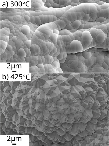
Figure 2. FESEM images of 300 cycles (a) amorphous TiO2 deposited at 300 °C and (b) polycrystalline TiO2 deposited at 425 °C.
Download figure:
Standard image High-resolution image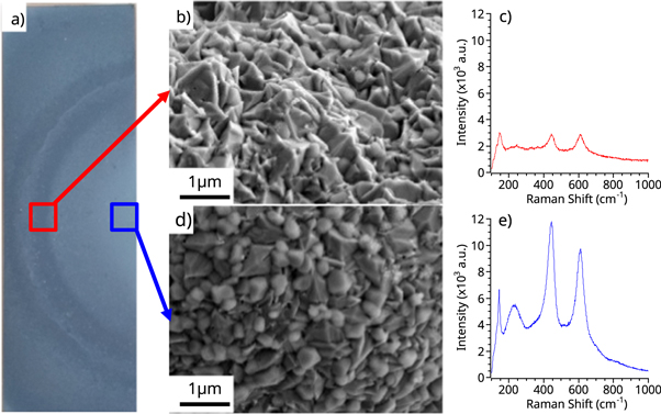
Figure 3. Characterization of the TiO2 crystallinity at 425 °C deposition temperature in two different sample location (edge and center), (a) optical image of a coated sample, (b) FESEM micrograph of the sample edge, (c) Raman spectra of the sample edge, (d) FESEM micrograph of the sample center, (e) Raman spectra of the sample center.
Download figure:
Standard image High-resolution imageA small amount of TiO2 powder also formed on the dispersion lid, suggesting the need to increase the TiCl4 precursor concentration while keeping the water concentration constant. Since Raman spectra of the samples with 150 cycles display the presence of anatase crystals, the number of cycles for the following tests was decreased to 120 and 60. Also, the reactor temperature of 425 °C was kept constant for the rest of the experiments. The precursor concentration effect was studied by only increasing the TiCl4 pulse from 25 ms up to 100 ms. Table 2 summarizes all other parameters.
Table 2. Deposition parameters used to observe the effect of the precursor pulse.
| TiCl4 | H2O | |
|---|---|---|
| Pulse (ms) | 25–80 | 30 |
| Wait (s) | 3–5 | 1.5 |
| Vacuum (s) | 2 | 2 |
| Flow Rate(sccm) | 50 | 50 |
| Bottle Temp. (°C) | 40 | 27 |
| Reactor Temp.(°C) | 425 | |
| Line Temp. (°C) | 150 | |
| Cycles n | 120 and 60 | |
Figure 4 shows the Raman spectra of different 60 cycles runs conducted at increasing TiCl4 precursor pulse times. Based on figure 4, the anatase crystal phase concentration is proportional to the TiCl4 precursor pulse duration. Also, a transition from the rutile-anatase mixture to pure anatase happens at approximately 60 ms. After 60 ms, the anatase peaks intensity increased, demonstrated by the development of the vibrational mode at 198 cm−1, and plateau at 80 ms. Under the same conditions, samples coated for 120 and 60 cycles exhibit no major difference in their Raman spectra, suggesting that 60 cycles can produce pure polycrystalline anatase TiO2. Since the 80 ms precursor pulse produced samples with a clean anatase Raman spectrum, it was selected as an optimal TiO2 precursor pulse time.
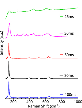
Figure 4. Raman spectra of polycrystalline TiO2 growth for 60 cycles as a function of the TiCl4 precursor pulse duration.
Download figure:
Standard image High-resolution imageRaman spectra of samples coated with 30 and 60 cycles are shown in figure 5. The TiO2 coating of these samples followed the parameters of table 2 and the variable waiting time of 3 to 5 seconds. An increased waiting time after the TiO2 precursor pulse it produced an increased intensity of the anatase peaks between 3 and 4 seconds with minimum gain afterward.
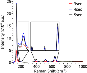
Figure 5. Raman spectra of polycrystalline TiO2 growth for 60 cycles as a function of the TiCl4 precursor waiting time duration.
Download figure:
Standard image High-resolution imageFigure 6 shows FESEM images and Raman spectra of the semi-circular samples coated with the parameters, shown in table 3, identified earlier to produce anatase TiO2. The 144, 394, 514, and 636 cm−1 peaks suggest an anatase TiO2 phase. The percentage of [001] surfaces present was calculated as 8 ± 1.7%, for both 30 and 60 cycles. The percentage of the [100] surfaces was obtained by the peak intensity ratio of the 144 cm−1 and 514 cm−1 peaks [31]. The Raman spectra in figure 6 show an intensity reduction on all anatase peaks between the sample center, circle 1, and the edge, circle 2. However, there are no rutile peaks in either sample location, for both 30 and 60 cycles. The lower intensity of the anatase Raman signal can be explained by a reduced definition of the TiO2 crystals on the sample edges, as shown in the FESEM micrograph in figures 6(b) and (d). Also, Raman spectra of the 30 and 60 cycles showed no appreciable differences between the samples' center and edge. Outside of the circle, shown in figure 6, deposition and samples uniformity decreases.
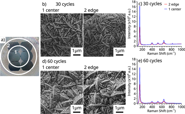
Figure 6. Characterization the TiO2 crystallinity of 30 and 60 cycles deposited at 425 °C (a)sample location in the deposition chamber, (b) and (c) FESEM micrographs and Raman spectra of the edge and center of 30 cycles samples, and (d) and (e) FESEM micrographs and Raman spectra of the edge and center of 60 cycles samples.
Download figure:
Standard image High-resolution imageTable 3. Deposition parameters used to observe the effect of the precursor pulse.
| TiCl4 | H2O | |
|---|---|---|
| Pulse (ms) | 80 | 30 |
| Wait (s) | 5 | 1.5 |
| Vacuum (s) | 2 | 2 |
| Flow Rate(sccm) | 50 | 50 |
| Bottle Temp. (°C) | 40 | 27 |
| Reactor Temp.(°C) | 425 | |
| Line Temp. (°C) | 150 | |
| Cycles n | 60 and 30 | |
Table 4 shows the overall composition, based on XEDS measurements, shown in supplementary information figures S2 and S3 available online at stacks.iop.org/NANOX/1/020030/mmedia, of the samples coated with 30 and 60 cycles of anatase TiO2. Titanium and oxygen concentrations are close to 60 and 40 percent, respectively, of TiO2. XEDS of the sandblasted substrate, shown in supplementary information figure S1, depicts a 68% of Ti and only 24% of O2. There is also a 6% content of silica attributed to residues from the glass abrasive used for sandblasting the samples. Table 4 also provides the TiO2 average mass gain and deposition rate per cycle. There is no statistical difference between the 30 and 60 cycles samples' deposition rates, an expected result since there are no changes in the deposition parameters except for the number of cycles. Also, the average mass gain of the 60 cycles sample is approximately double the average mass gain of the 30 cycle samples.
Table 4. Summary of the coating composition, deposition rate, mass gain, coating thickness (*estimated) crystal thickness and the gap between crystals as a function of the number of cycles.
| Cycles: | 30 | 60 |
|---|---|---|
| Ti(mass % /err. %) | 59.18/2.36 | 56.52/1.65 |
| O2(mass % /err. %) | 39.8/14.23 | 41.13/4.8 |
| Cl(mass % /err. %) | 0.1/0.03 | 1.37/0.07 |
| C(mass % /err. %) | 0.92/0.3 | 0.98 ± 0.2 |
| rate (mg/cycle) | 0.073 ± 0.005 | 0.068 ± 0.005 |
| mass(mg) | 2.2 ± 0.16 | 4.1 ± 0.3 |
| thickness*(nm) | 386 ± 28 | 720 ± 52 |
| gap (nm) | 110 ± 3.5 | 63 ± 2.5 |
| crystal width (nm) | 42 ± 1.9 | 38 ± 1.3 |
The thickness of the TiO2 coating was calculated based on the theoretical density of anatase TiO2. This thickness suggests a deposition per layer of ≈13 nm, suggesting that the growth mechanism is not the self-limited surface reaction of an ALD, but controlled by the process parameters more typical of a CVD or pulsed-CVD in this case. The thickness measured by cross-section microscopy, shown in figures 7(c) and (d), indicates a thickness of 864 ± 31 nm and 736 ± 59 nm in the center and edge respectively. The thickness differences between the center and edge are due to decreasing precursor concentration as a function of the chamber radius. There is a minimum difference between the crystal width of the 30 and 60 cycle samples. However, there is a ≈40% reduction in the gap between crystals as the number of cycles increase. Figure 7 better shows this difference between samples. The gap reduction can be explained by the increased number of nucleation spots from previous cycles, where new crystals begin to grow, and the preferential growth on the (101) direction.

Figure 7. High magnification FESEM images of samples coated with (a) 30, (b) 60 cycles, (c) cross-section of a 60 cycles sample edge, and (d) cross-section of a 60 cycles sample center.
Download figure:
Standard image High-resolution imageFinally, 3003 aluminum substrates, shown in figure 8, were coated with polycrystalline TiO2 following the parameters of table 3. The Al substrate samples were characterized via XRD and Raman, as shown in figure 9. The peaks 25.5° and 48.3° show a predominant (101) and (200), respectively, orientations of the anatase film. The (211) orientation is also strong in comparison with the (105) and (004) at 54° and 38°. No traces of rutile are observed in either XRD or Raman spectra. Thus, proving the reliability of the process to deposit polycrystalline anatase TiO2.
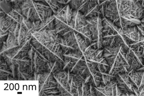
Figure 8. FESEM image of a 60 cycles polycrystalline TiO2 deposited on an aluminum substrate.
Download figure:
Standard image High-resolution image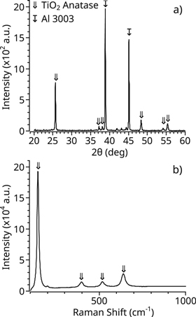
Figure 9. Polycrystalline TiO2 deposited on an aluminum substrate (a) XRD, and (b) Raman spectra.
Download figure:
Standard image High-resolution image
4. Conclusions
Deposition parameters of an ALD system were refined to create growth conditions wherein reactants were never fully purged from the chamber, resulting in a pulsed-CVD. The final parameters produced an anisotropic growth and the formation of highly defined 3D polycrystalline morphologies. Under these conditions, crystalline anatase phase titania was attained in as few as 30 cycles, without requiring subsequent annealing. Thus, suggesting that the attainment of polycrystalline anatase TiO2 is highly dependant on process conditions. Raman and XRD spectroscopy exhibit no trace of amorphous or rutile titanium dioxide on the 30 nor 60 cycles samples. XEDS revealed traces of Cl and C. There was a minimum difference in the polycrystalline deposition thickness between 30 and 60 cycles. However, the gap between crystals decreases more than 40% on the 60 cycles samples, implying that the mass gain from 60 to 30 cycles is due to increased nucleation of new crystals and the preferential growth along the (101) direction. The highly defined crystal structure and size in the reduction from 60 to 30 cycles suggest that these pulsed-CVD process conditions could produce a similar crystal size and anatase structure at even fewer cycles. Finally, the achievement of anatase on aluminum substrates at the same number of cycles as that on titanium suggests that these same process conditions could effectively coat other materials with similar success to that seen on titanium.
Acknowledgments
The authors thank the Center for Advanced Microscopy and Imaging at Miami University, Dr. Andre Sommer at the Molecular Microspectroscopy Laboratory at Miami University, and Dr. John Rakovan from the Department of Geology and Environmental Earth Science for their assistance.
Data Availability
The data that support the findings of this study are available upon reasonable request from the authors.