
Abstract
PbS nanoparticles and CdS nanoparticles are grown by chemical methods. Also bulk PbS is grown by simple chemical methods without using any capping agent. The material formation is identified from XRD.TEM image shows the formation of different shaped PbS nanoparticles, CdS nanoparticles, and bulk PbS. Three different heterojunction solar cells are fabricated by CdS and PbS samples using a spin coating technique. Finally, gold is evaporated on PbS film. Current-voltage characteristics data for three heterojunction solar cells are taken under dark and illumination conditions. For each fabricated solar cell open-circuit voltage (VOC), short circuit current density (ISC), fill factor (FF), and power conversion efficiency( ) are measured. Finally, a comparison of the characteristics is done for different fabricated heterojunction solar cells.
Export citation and abstract BibTeX RIS

Original content from this work may be used under the terms of the Creative Commons Attribution 4.0 licence. Any further distribution of this work must maintain attribution to the author(s) and the title of the work, journal citation and DOI.
1. Introduction
Lead sulfide nanoparticles are perfect optoelectronic material [1–3]. PbS nanoparticles have an exciton Bohr radius of 18 nm and an optical cut-off of 3020 nm [4–6]. The absorption band of Lead sulfide belongs to the near-infrared region of the solar spectrum [7]. PbS is a direct band-gap semiconductor [8]. The bandgap of PbS nanoparticles is tuned by growing different sizes due to the quantum confinement effect [9–11]. PbS nanoparticles have huge efficiency in the formation of low- cost photovoltaic devices [12–14]. CdS nanoparticles have an optical cut-off of 515 nm with an exciton Bohr radius of 6 nm [15]. Cadmium Sulfide is a popular semiconductor nanoparticle as its direct band-gap which is located in the visible region [16–18]. So photodetectors and solar cell is made from CdS nanoparticles. Organic bulk heterojunctions solar cells also experience lower carrier diffusion lengths and large offsets in the donor and acceptor levels in the semiconductor. Power conversion efficiency is enhanced by the multi exciton generation by PbS nanoparticles [19–21]. Now a narrow layer of large bandgap (2.4 eV) CdS nanoparticles are introduced to the surface of PbS samples to control trap states caused by lattice imperfections on the surface [22–25]. Here we fabricate a p-n junction solar cell made of a p-type PbS nanoparticles layer on top of an n-type CdS nanoparticles layer. The electron-hole pair production per photon is about 2.4 for PbS nanocrystal-based devices [26]. PbS nanocrystals lose no extra energy to thermalization for converting high-energy photon generation by creating multiple electron-hole pairs [27]. Materials are produced by chemical method because it is simple to maintain the time of reaction, temperature, stirring period, pH of the solution, and complexing agent [28]. Jie Jiao et al [29] used FTO/TiO2/CdS/PbS as photoelectrode in Quantum dot-sensitized solar cells (QDSSCs). It produced light to electric power conversion efficiency (Eff) of 2.0% under AM 1.5 illumination (100% sun), Jsc value was 18.8 mA cm−2, Voc value was 0.31 volt, and fill factor was 34.3. This showed the best power conversion efficiency compared with single CdS or PbS sensitized QDSSC. M J Speirs et al [30] demonstrated solar cells made from PbS–CdS core–shell QDs, yielding a 147 mV increase in VOC compared to core only PbS QDs with an efficiency of nearly 2.5%, Jsc value was 10 mA cm−2, Voc value was 0.59 volt and fill factor was 44. M Masood et al [31] used PbS quantum dot as light absorber material and simulated a PbS quantum dot sensitized solar cell which had a power conversion efficiency of 1.8%, Jsc value was 12.3 mA cm−2, Voc value was 0.33 volt and fill factor was 44. M A K L Dissanayake et al [32] fabricated solar cells with TiO2 nanofiber/TiO2 nanoparticle double-layer photoanode sensitized with PbS/CdS core–shell structure of efficiency 3.55% Jsc value was 12.07 mA cm−2, Voc value was 0.63 volt and fill factor was 46.67 whereas efficiency was 4.09%, Jsc value was 14.85 mA cm−2, Voc value was 0.627 volt and fill factor was 43.9 by incorporating Ag nanoparticles into the TiO2 nanostructure.
In the present work, PbS nanoparticles and CdS nanoparticles are grown by chemical reduction route. But bulk PbS are grown by the chemical method without using any capping agent. Finally, three heterojunctions are fabricated between CdS nanoparticles and two different shaped PbS nanoparticles as well as with bulk PbS. Finally, all solar cell parameters of three heterojunctions are compared.
2. Experimental
2.1. Sample preparation
Lead chloride, Sulfur powder, Ethylene Diamine, and Sodium borohydride reagents were used to produce nanoparticles of PbS. Ethylene Diamine used as a capping agent. Lead chloride was mixed in Ethelyne Diamine and stirred for a few minutes at 1000 RPM. We added the sulfur powder in it. NaBH4 was added after a few minutes of stirring. Samples were then stirred for 4 h and collected for centrifuge at 2000 RPM. Next, the samples were thoroughly washed and dried to get a powder sample of PbS nanoparticles. When Lead chloride, Sulfur powder, and Sodium borohydride were mixed in 1:1:1 ratio, the shape of grown PbS nanoparticles were spherical whereas for 1:1:3 ratio, the shape of PbS nanoparticles were cubic. Also for CdS nanoparticles, the proper amount of CdCl2 was taken in Ethelyle Diamine and the same process was repeated. To grow bulk PbS, Pb(C2H3O2)2.3H2O and Thiourea were taken in a beaker with proper ratio and its pH (11) was maintained by adding NH4OH. Thus in bulk PbS preparation, we did not use any capping agent like Ethelyne Diamine.
2.2. Sample characterization
X-ray diffraction (XRD) of powder samples is done with High- resolution Rigaku Mini Flex x-ray Diffractometer for range 20 to 70 degrees for PbS samples and 5 to 50 degrees for CdS sample.JEOL-JEM 2100 HRTEM is used to get TEM images of PbS samples and CdS samples using the carbon-coated copper grid. To get absorption spectra powder samples are ultrasonicated in ethanol medium. Change in absorption intensity with wavelength is obtained by Agilent Technologies Cary 5000 Series UV–vis-NIR Spectrophotometer. From optical absorption spectra in Visible and NIR-region, the bandgap is determined for PbS nanoparticles, CdS nanoparticles, and bulk PbS.
2.3. Heterojunction fabrication and characterization
Powder samples are sonicated in Ethanol for one hour. Indium tin oxide (ITO) coated glasses were purchased having a sheet resistance of 10 Ω per square inch. The ITO coated glass slide of size (2.5 cm × 2.5 cm) is covered with Teflon by ¼ area and was kept at the center of the spin coater using vacuum. After the vacuum is confirmed CdS drops are pushed by syringe on ITO coated glass rotating at 2500 RPM. CdS nanoparticles are deposited partly on pre-cleaned ITO coated glass. Thereafter PbS samples are deposited on CdS layer by the same process. Finally, for ohmic contact, gold is thermally evaporated and deposited on PbS film by the shadow mask. The size of the gold dot is 0.03 cm2. The schematic diagram of heterojunction is shown in figure 5. The current with a change in voltage measurement is done with a semiconductor parameter analyzer Agilent 4155. The current and voltage measurement is taken under dark and global 1.5 AM solar irradiation which is equal to 100 mW cm−2.
3. Results and discussion
3.1. Structural analysis
The XRD pattern of PbS nanoparticles, bulk PbS, and CdS nanoparticles are shown in figure 1

Figure 1. XRD pattern of (a) spherical PbS (b) cubic PbS (c) bulk PbS and (d) CdS nanoparticles.
Download figure:
Standard image High-resolution imageXRD pattern confirmed the formation of PbS and CdS nanoparticles. The cubic phase of grown samples is identified from the diffraction pattern matched with the standard JCPDS database. The XRD data shows crystallinity along (200) direction in PbS samples. The particle size of samples is measured from the TEM image and the shape of the particle is seen clearly.
TEM images of different shape PbS nanoparticles, bulk PbS and CdS nanoparticles are shown in figure 2.
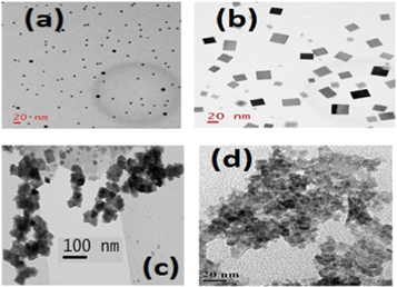
Figure 2. TEM images of (a) spherical PbS (b) cubic PbS (c) bulk PbS and (d) CdS nanoparticles.
Download figure:
Standard image High-resolution imageThe size of CdS nanoparticles is found to be 12 nm using a TEM pattern. The average particle sizes of spherical shape, cubic shape, and bulk PbS are found to be 8 nm, 11nm, and 45 nm respectively. The spherical and cubic shaped nanoparticles of PbS are well isolated in TEM pattern whereas bulk PbS are found to be agglomerated. CdS nanoparticles show a chain like a pattern in the TEM image.
3.2. Optical characterization
Optical absorption spectra of PbS nanoparticles, bulk PbS, and CdS nanoparticles are shown in figure 3.
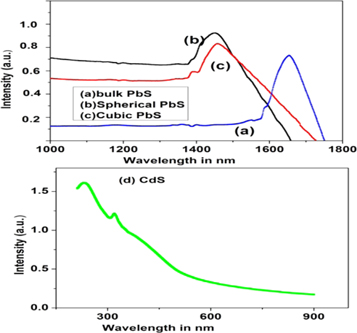
Figure 3. Optical absorption spectra of (a) bulk PbS (b) spherical PbS (c) cubic PbS and (d) CdS nanoparticles.
Download figure:
Standard image High-resolution imageBoth PbS and CdS samples are dispersed in ethanol by sonicator for 45 min. Samples are taken in a quartz cuvette for which light of all wavelength travels the equal path of 1 cm thickness for each dispersed sample. The optical absorption is taken in the wavelength region from 1000 nm to 1800 nm for PbS samples whereas it is taken in the wavelength region from 200 nm to 900 nm for CdS sample. The absorption coefficient is related with photon energy by this relation, (αhν)n = k(hν − Eg) where K is constant, hν is the photon energy, α is the absorption coefficient, n is a constant which may be a different value for different transitions obeying well-defined selection rules, and it denotes the nature of electronic transition responsible for absorption. For directly allowed transition n is 2, for directly forbidden transition n is 3, for indirectly allowed transition n is1/2, for indirect forbidden transition n is 1/3. The best fit is obtained for the graph of (αhν)2 versus hν which is known as Tauc plot and, the extrapolation of the graph to the x-axis will give the bandgap energy.
Bandgap determination plot of bulk PbS, Spherical PbS, cubic PbS, and CdS nanoparticles are shown in figure 4.
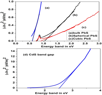
Figure 4. Band gap determination plot of (a) bulk PbS (b) spherical PbS (c) cubic PbS and (d) CdS nanoparticles.
Download figure:
Standard image High-resolution imageSpherical and cubic shaped PbS nanoparticles have bandgap energy 1.04 eV, 0.91 eV respectively, while bulk PbS band gap is found to be 0.6 eV. CdS nanoparticles have bandgap 2.52 eV as evident from figure 4. The absorption edge shift towards lower wavelength as particle size decreases in quantum size effect [33, 34]. Thus bandgap increases due to the quantum confinement effect both for CdS and PbS nanoparticles. Therefore band edge shifts towards shorter wavelength for both of these nanoparticles.
3.3. Solar cell analysis
The mismatch of the lattice constant of composite materials must be minimum for the fabrication of heterojunction solar cells. Also, the difference in lattice constant between CdS and PbS is 0.165 A0, which is small. That's why PbS is suitable for the fabrication of heterojunction solar cells with CdS.
The block diagram of heterojunction solar cells fabricated using CdS and PbS nanoparticles or bulk PbS is shown in figure 5.

Figure 5. Block diagram of heterojunction solar cells fabricated using CdS and either PbS nanoparticles or bulk PbS.
Download figure:
Standard image High-resolution imageThe vacuum level is the energy of free electron just outside the neutral semiconductor. The location of the conduction band (CB) and valence band (VB) are determined by the chemical bonding of atoms. The energy required to free electron from the conduction band of a semiconductor is known as electron affinity (χ). The work function (ϕ) is defined as the energy required to free-electron from the Fermi level (Ef) of a semiconductor. The built-in potential (Vbi) magnitude is expressed in the volt unit as a difference in the work function for n-type and p-type semiconductors. The work function (ϕp) of the p-type semiconductor is given as (χP + EGP–δP) where δP = (EFP − EV). The work function (ϕN) of the n-type semiconductor is given as (χN + δN) where δN = (EC-EFN). The standard value of electron affinity and work function for PbS and CdS nanoparticles are used to calculate the built-in potential for heterojunctions. Electron affinity value of CdS nanoparticles, spherical PbS, Cubic PbS nanoparticles, and bulk PbS is taken as 4.7 eV, 4.5 eV, 4.55 eV, 4.6eV. Work function of CdS nanoparticles, spherical PbS, Cubic PbS nanoparticles, and bulk PbS semiconductor assumed as 4.9eV, 5.1eV, 5.25eV and 5.35 eV [25, 35, 36].
The built-in potential, Valence band discontinuity, and Conduction band discontinuity for three heterojunctions solar cell are given in table 1.
Table 1. Data of the Conduction band discontinuity, Valence band discontinuity, and built-in potential for three heterojunctions solar cell.
| Heterojunction Solar Cell | ΔEC(eV) | ΔEV(eV) | Vbi (V) |
|---|---|---|---|
| CdS/Spherical PbS | 0.2 | 1.68 | 0.45 |
| CdS/Cubical PbS | 0.15 | 1.76 | 0.35 |
| CdS/Bulk PbS | 0.1 | 2.02 | 0.2 |
Band diagrams of n-type and p-type semiconductors before contact, Fermi level configuration, and built-in potential across the depletion region of heterojunction consisting of n-type CdS and p-type PbS is shown in figure 6.

Figure 6. Band diagrams of (a)–(c) n-type and p-type semiconductors before contact, (d)–(f) Fermi level configuration and built-in potential (Vbi) across the depletion region of heterojunction.
Download figure:
Standard image High-resolution imageThe dark current density(J in mA cm−2) –voltage(V in volt) characteristics of three heterojunction solar cells fabricated using CdS nanoparticles and PbS nanoparticles as well as bulk PbS are shown in figure 7.
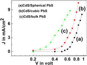
Figure 7. The dark current density(J in mA cm−2) –voltage(V in volt) characteristics of three heterojunction solar cells fabricated using (a) CdS and spherical PbS nanoparticles (b) CdS and cubic PbS nanoparticles (c) CdS nanoparticles and bulk PbS.
Download figure:
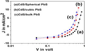
Standard image High-resolution imageThe current density(J in mA cm−2)–voltage(V in volt) characteristics of three heterojunction solar cells fabricated using CdS nanoparticles and PbS nanoparticles as well as bulk PbS under global 1.5 AM solar irradiation are shown in figure 8.
Figure 8. The current density(J in mA cm−2) –voltage(V in volt) characteristics of three heterojunction solar cells fabricated using (a) CdS and spherical PbS nanoparticles (b) CdS and cubic PbS nanoparticles (c) CdS nanoparticles and bulk PbS under global 1.5 AM solar irradiation.
Download figure:
Standard image High-resolution image
Current density-Voltage data for three heterojunction solar cells are collected in dark and light conditions. The dark saturation current is the largest for CdS nanoparticles and bulk PbS material and decreases with the size of nanoparticles. The reduction of JSC (from 7.6 mA cm−2 to 6.6 mA cm−2) may be due to a decrease in the light absorption with an increase of the bandgap for smaller size PbS nanoparticles strongly indicating the quantum confinement effect [14]. Another reason for decreasing in the short circuit current density may be due to series resistance created by a high density of surface traps within the bandgap of PbS nanoparticles [22, 23]. The bandgap is increased in PbS nanoparticles than bulk PbS which increases the open-circuit voltage by reducing the electron-hole recombination rate [37, 38]. Also, open-circuit voltage (Voc) increases for heterojunction fabricated with higher bandgap PbS materials for a high density of surface traps in the bandgap [24, 25]. The fill factor (FF) was determined from the following equation FF = (Jm × Vm)/(Jsc × Voc), Where Jm is maximum current density and Vm is representing maximum voltage. Again Jsc is the short circuit current density and Voc is the open-circuit voltage. Also, the energy conversion efficiency is given by  = FF×(Jsc × Voc)/Pin where Pin represents the input power of radiation. The highest efficiency is obtained by 1.98% for heterojunction solar cells of CdS/spherical shaped PbS nanomaterials. Solar cell device made by CdS nanoparticles and bulk PbS gives efficiency 1.05% because of grain boundary effect. Hence efficiency sharply increases for nanoparticles of PbS as compared to bulk form. This is possible due to the increase of surface area in the case of Pbs nanoparticles compared to bulk PbS. The weak photovoltaic performance of the CdS/bulk PbS heterojunction may be prohibited by the built-in voltage.
The observed solar cell parameters, short circuit current density (Jsc), Fill factor (FF), efficiency, and sample characteristics are given in table 2.
Table 2. The observed solar cell parameters, short circuit current density (Jsc), Fill factor (FF), efficiency, and sample characteristics.
| Sample | Vmax(V) | Jmax (mA cm−2) | JSC (mA cm−2) | Voc(V) | FF (%) | Efficiency (%) |
|---|---|---|---|---|---|---|
| CdS/Spherical PbS | 0.45 | 4.4 | 6.6 | 0.64 | 46.8 | 1.98 |
| CdS/CubicPbS | 0.3 | 4.8 | 7.4 | 0.5 | 38.9 | 1.44 |
| CdS/BulkPbS | 0.25 | 4.2 | 7.6 | 0.46 | 30 | 1.05 |
4. Conclusion
Spherical, cubic PbS, CdS nanoparticles, and bulk PbS are grown by a simple chemical method. TEM pictures show spherical and rectangular-shaped nanoparticles. These are grown using different reducing agent ratio. Optical absorption spectral analysis shows that spherical nanoparticle has higher bandgap due to quantum confinement effect as compared to bulk PbS. The efficiency of heterojunction devices grown from spherical PbS and CdS nanoparticles show the highest efficiency. Efficiency decreases with the increase of particle size. We get power conversion efficiency ( ) of heterojunction solar cells based on CdS nanoparticles and bulk PbS is 1.05% and whereas heterojunction solar cells based on CdS nanoparticles, and spherical PbS nanoparticle is 1.98%. Thus power conversion efficiency (
 ) of heterojunction solar cells is higher consisting of smaller PbS nanoparticles.
Acknowledgments
Authors are grateful to UGC & DST for their constant support through SAP and FIST program to the Department of Physics, Vidyasagar University.