
Abstract
Precise spatial control of 2D materials is the key capability of engineering their optical, electronic, and mechanical properties. However, growth of novel 2D Mo2C on Cu surface by chemical vapor deposition method was revealed to be seed-induced 2D growth, limiting further synthesis of complex Mo2C spatial structures. In this research, we demonstrate the controlled growth of Mo2C pyramids with numerous morphologies, which are characterized with clear terraces within the structures. The whole evolution for Mo2C pyramids in the coursed of CVD process has been detected, posing significant potential in probing growth mechanism. The formation of the Mo2C pyramids arises from the supersaturation-induced nucleation and concentration-gradient driven diffused growth of a new Mo2C layer on the edged areas of intrinsic ones, as supported by STEM imaging. This work provides a novel Mo2C-based pyramid structure and further reveals a sliding growth mechanism, which could offer impetus for the design of new 3D spatial structures of Mo2C and other 2D materials.
Export citation and abstract BibTeX RIS
1. Introduction
2D materials provide unusual mechanical, chemical, and electronic properties that can be influenced by their spatial structures[1-3]. As a new member of 2D materials, Mo2C has been gaining great strengthen in the past few years because of its potential applications in energy storage and catalysis and so on[4-8]. Recent advances in chemical vapor deposition (CVD) methods have enabled the large-scale production of high-quality 2D Mo2C crystals[9-11]. Meanwhile, interesting Mo2C/graphene vertical heterostructure has been achieved by a one-step CVD process[12-14]. However, there still exist several issues to be resolved. Currently, the CVD method in shaping Mo2C have fundamental limitations that are based on a seed-induced 2D growth mechanism[8] and do not allow one to fabricate in situ complex spatial Mo2C structures during the growth process. Moreover, the detailed mechanism for Mo2C formation during CVD is less explored and the related kinetics process is still elusive. The lack of understanding on the growth mechanism of Mo2C has hindered further studies of their intrinsic properties and wide applications.
Here we demonstrate spatially controlled growth of large-area Mo2C pyramid structures on liquid Cu surface by ambient pressure CVD method. A large amount of carbon atoms has been introduced as an accelerator to bond with Mo atoms to achieve the structures. Clear observations of terraces and highly symmetrical regular shaped contours under atomic force microscope (AFM) characterization reveal the existence of pyramid features in the as-grown Mo2C. An inside-out lateral diffusion mechanism was proposed to elucidate the formation process as supported by atomic-resolution transmission electron microscopy (ARTEM) imaging. The proposed inside-out growth model provides a general guide for engineering spatial growth of 2D materials. This approach stands as a complementary method to CVD growth while permitting growth of complex Mo2C based spatial structures.
2. Experimental section
2.1. CVD growth of Mo2C pyramids
A Cu foil (Alfa Aesar, 99.9% purity, 25 μm thick) was cut into 10 × 10 mm2 pieces and placed on top of a Mo foil (Alfa Aesar, 99.95% purity, 50 μm thick) of the same size. They were then placed in a quartz tube of outer diameter 25 mm, inner diameter 22 mm and length 1220 mm to act as catalyst for growth of Mo2C pyramid structures. Subsequently, the substrates were heated above 1100 °C in a horizontal tube furnace (Lindberg Blue M, TF55030C) under 200 sccm H2 and then kept for 30 min for annealing. Certain gas flow rate of CH4 was then introduced into the chamber at ambient pressure to initiate the growth. After the reaction, the samples were quickly removed from the high-temperature zone under H2, to ensure rapid cooling of the samples to room temperature.
2.2. Transfer of Mo2C pyramids structures
Poly(methyl methacrylate) (PMMA)-assisted chemical etching method was used. A thin layer of PMMA (weight-averaged molecular mass Mw = 600 000, 4 wt% in ethyl lactate) was first spin-coated on the surface of Mo2C crystals at 6000 r.p.m. for 3 min and cured at 170 °C for 5 min; the PMMA-coated samples were immersed into a 1 M (NH4)2S2O8 aqueous solution for etching the underneath Mo and Cu substrates. Then the PMMA/Mo2C layer was detached from the substrate after several minutes. After cleaning with pure water, the floating PMMA/Mo2C layer was stamped at the target substrate, such as SiO2/Si and TEM grids. Finally, the PMMA was removed by warm acetone, obtaining clean ultrathin Mo2C pyramids.
2.3. Characterization
Optical images were obtained using an Olympus BX51 microscopy. AFM images were obtained using a Bruker Dimension FastScan Atomic Force Microscope in the tapping mode. XPS analysis was carried out on an Omicron EAC2000-125 analyzer. Base pressure during analysis was 9−10 Torr. An Al Kα monochromatized radiation (hν = 1486.6 eV) was employed as the X-ray source. Raman spectra were recorded at room temperature using a WITec Raman Microscope with laser excitation at 532 nm. Bright filed TEM images of Mo2C structures were conducted on Philips CM30 TEM at 300 kV. High resolution STEM ADF imaging was carried on an aberration-corrected Nion UltraSTEM-100, equipped with a cold field emission gun, operating at 100 kV for Mo2C samples.
3. Results and disscussion
The whole growth process is schematically shown in Fig. 1. It is seen that during the CVD growth, the CH4 is introduced into the chamber as carbon source, while several pieces of Cu foils sitting on a Mo foil as the substrate at a temperature of 1150 °C (see Methods). Note that, the high temperature (above melting point of metal Cu) allows the Cu into liquid phase[15-17], thus facilitating Mo atoms to diffuse from Cu-Mo interface to the surface of Cu to form Mo2C. Unlike with the previously reported growth[9, 10] in our case, after segregation of Mo atoms onto the Cu surface, the high temperature and large flow rate of CH4 enables excessive segregation of Mo atoms, leading to large-area growth of typical Mo2C pyramids with obvious featured terraces.

Fig. 1 (Color online) Schematic showing the growth of Mo2C pyramids on liquid Cu substrate.
Download figure:
Standard imageFig. 2(a) shows the optimized crystal structure of Mo2C. Mo2C holds an orthorhombic structure with space group Pbcn. The optimized lattice contants are 4.77, 5.99, and 5.21 Å, respectively. From the top view, Mo2C shows regular hexagonal profile like MoS2, MoSe2 and many other layered 2D materials. From the side view, each Mo (C) atomic layer is combinedly bonded by two C (Mo) layers. The first-principles calculations are performed to explore its electronic structure in Figs. 2(b) and 2(c). It is found that both the electronic bands near the Fermi level are mainly contributed by d orbitals of Mo. The rather delocalization of electrons near the Fermi level makes Mo2C a metal. Fig. 2(d) shows the Mo2C pyramid structures fabricated on liquid Cu surface at 1150 °C under 0.2 sccm methane, 50 sccm hydrogen and 300 sccm argon with a growth time of 60 min. Notably, the argon has been introduced as tunable gas, facilitating decomposition of the methane during the growth process[18]. The large-area growth of Mo2C pyramid-like structures (Fig. S1) suggested that a general growth rule might work in shaping Mo2C and the detailed growth mechanism will be present in the following section. In our experiments, it is found that all the pyramid structures have highly symmetrical shapes, a typical characteristic of well-defined crystals. As for the central part within the pyramid structures, obvious hexagonal profile is observed and thus results in formation of terrace with respect to the outer one. All the Mo2C pyramid structures in Fig. 2(d) have regular hexagonal profiles, indicating as-formed terraces with respect to Cu substrate. It is worth noting that the Mo2C pyramid structures with terraces is first demonstrated, which is largely different from the as-reported Mo2C with the same thickness among the whole flake[8, 11]. Further, the large-area growth of those pyramid structures strongly confirms the high controllability of our method over spatial stacking of 2D materials.

Fig. 2 (Color online) Growth and characterization of Mo2C pyramids. (a) Crystal and (b, c) electronic structure of Mo2C from first-principles calculations. (d) Optical images of grown Mo2C pyramids structures on liquid Cu surface. (e, f) XPS spectra of Mo2C flake, indicating existence of Mo and C, respectively. (g–i), AFM images of three typical layered pyramids structures.
Download figure:
Standard imageX-ray photoelectron spectroscopy (XPS) has been performed to probe the element information of the as-grown Mo2C crystals. It is obviously found (Figs. 2(e) and 2(f)) that there exist two typical signals correlated with the corresponding elements C and Mo, respectively. It should be noted in Fig. 1(b) that the peak derived from the C–Mo bond is labeled, indicating the flake is composed of Mo and C with an atomic ratio of ~2 : 1.
After CVD growth, a mild Cu etchant, (NH4)2S2O8 (see Methods) is used for transferring Mo2C flakes, similar to the transfer CVD-grown other 2D materials[19]. AFM images of three transferred hexagonal layered Mo2C structures are clearly shown in Figs. 2(g)–2(i). As for each structure, the size of inner hexagonal profile is much smaller than that of outer one. Terrace is formed at the edge of inner flake, serving as an indicator of thickness. In the three Mo2C structures, hexagonal shapes are strictly kept, suggesting a certain growth mode.
Fig. 3(a) shows typical optical images of large-area as-transferred Mo2C flakes on SiO2/Si substrate, exhibiting a clear color contrast. Further characterizations show different colors on Cu surface or SiO2/Si substrates, allowing rapid thickness identification. Raman mapping measurement has been conducted on the Mo2C structure. It is evidenced that the Mo2C pyramid structures owns a characterized peak at around 650 cm–1 under Raman spectrum (Fig. 3(b)), highly related with the orthorhombic crystal structure of Mo2C, corresponding to the stretching mode of Mo–C. From the mapping image, three hexagonal profiles are clearly found (Fig. S2), further confirming the pyramid structures of the Mo2C flake. Uniform color contrast among the layered whole structure is observed, indicating the same feature for the three composed hexagonal parts. Based on Raman analysis, it is reasonably deduced that the pyramid structure is composed of three individual parts along lateral direction, rather than three hexagonal flakes via layer-by-layer mode along vertical direction.
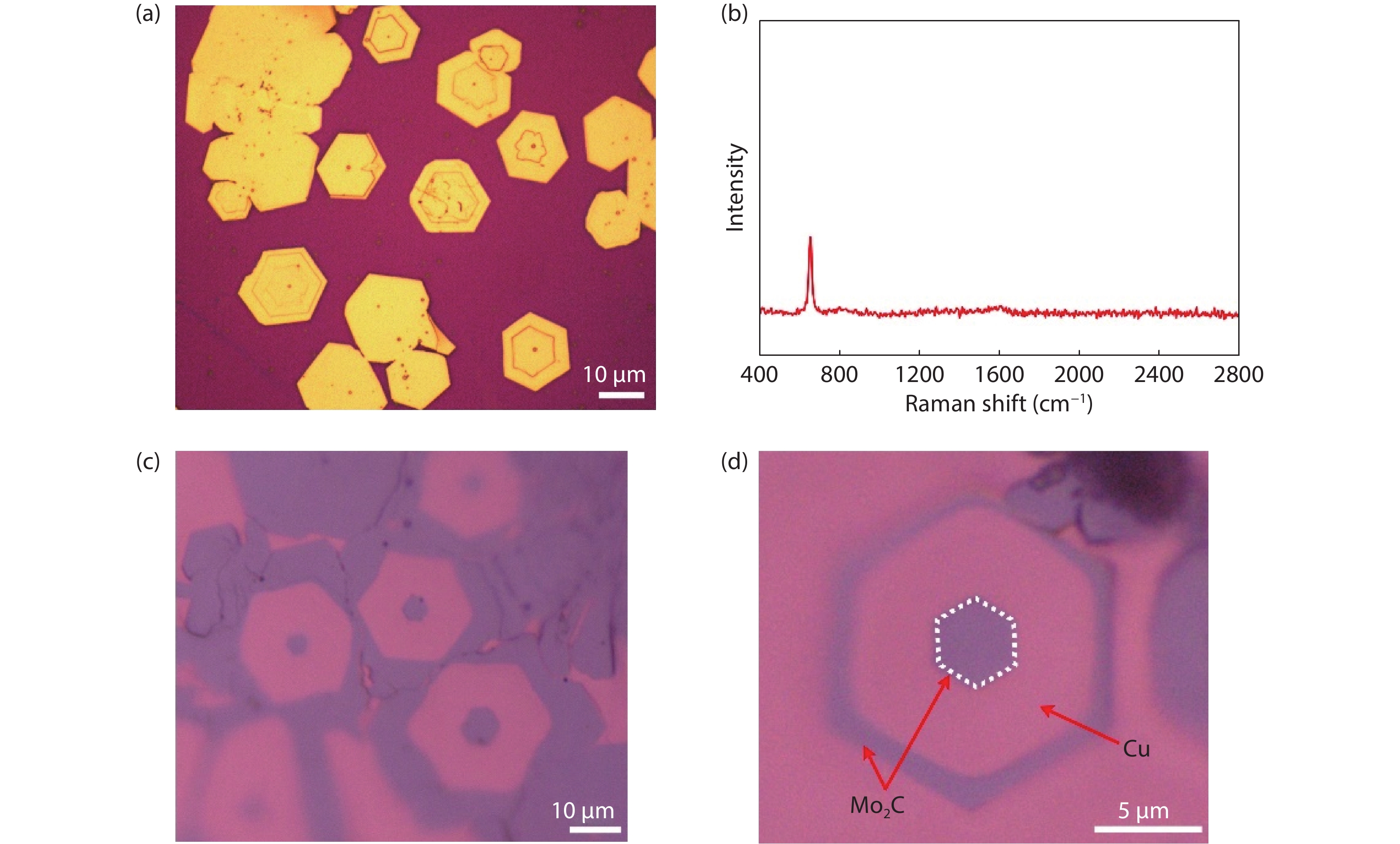
Fig. 3 (Color online) Further characterization and proposed model of Mo2C pyramid structures. (a) Optical images of grown layered Mo2C structures on liquid Cu surface and SiO2/Si substrate. (b) Raman spectrum of Mo2C flake, having characterized peak at around 650 cm–1. (c, d) Optical image of broken layered Mo2C structure, with bare hexagonal profile of Cu left.
Download figure:
Standard imageIn our experiments, one interesting phenomenon is detected, posing implication on growth mechanism of hexagonal Mo2C pyramid. The inner hexagonal part of the pyramid structures occasionally drops off during the growth or transferring process, with incomplete hexagonal profile left. Further analysis shows that the middle part falls off independently with a hexagonal loop profile, with the bare Cu surface left behind, while the inner part and outer part still keep intact (Figs. 3(c) and 3(d)). On the basis of the observations, it is suggested that the growth of Mo2C pyramid structures does not follow a layer-by-layer behavior, whereas week interlayer force enables peeling off through layer-by-layer and thus results in the intact downside layer even dropping of the topside layer. Then an inner-outside growth mode is favorable, in which the center part is highly initialized by excessive segregation of Mo atoms, after that, driven by concentration gradient, the following growth takes place from inside to outside with a decreasing thickness. Under this circumstance, the above experimental observations are feasible.
Another clue involving left residues during transferring process further confirms the second growth mode. After transferring of the Mo2C pyramid onto SiO2/Si substrates, with the structures falling off, the whole hexagonal profile, especially the contour of inner part, are kept, showing clear terraces, similar with those structures on Cu surface (Fig. S3). The stamp phenomena only appear under the second growth mode, while in the first case, it will cause the whole uniform profile on the SiO2/Si substrates. Based on the above discussion, it is deduced that the second growth mechanism works, resulting in the formation of novel hexagonal Mo2C pyramid structures.
Moreover, direct observation of the novel growth process of Mo2C pyramids is realized. In our CVD growth, another kind Mo2C pyramid structure is also controllably prepared through lowering flow rate of hydrogen to 10 sccm, whereas the profile of center part exhibits six-folded star shape, while the outer part still owns hexagonal profile. The large-area structures have been obtained over the whole substrate as shown in Fig. 4(a) and Fig. S4(a). It is clearly seen that most of those Mo2C pyramids are similar with each other, indicating a uniform growth process. Similar with the former hexagonal case, the novel star-shaped structures also exhibit a relatively high contrast with the substrate, indicating a thickness range. The thickness determination has been performed on the as-transferred samples as shown in Fig. 4(b), whereas a distinctive terrace was detected along the central star-shaped area.
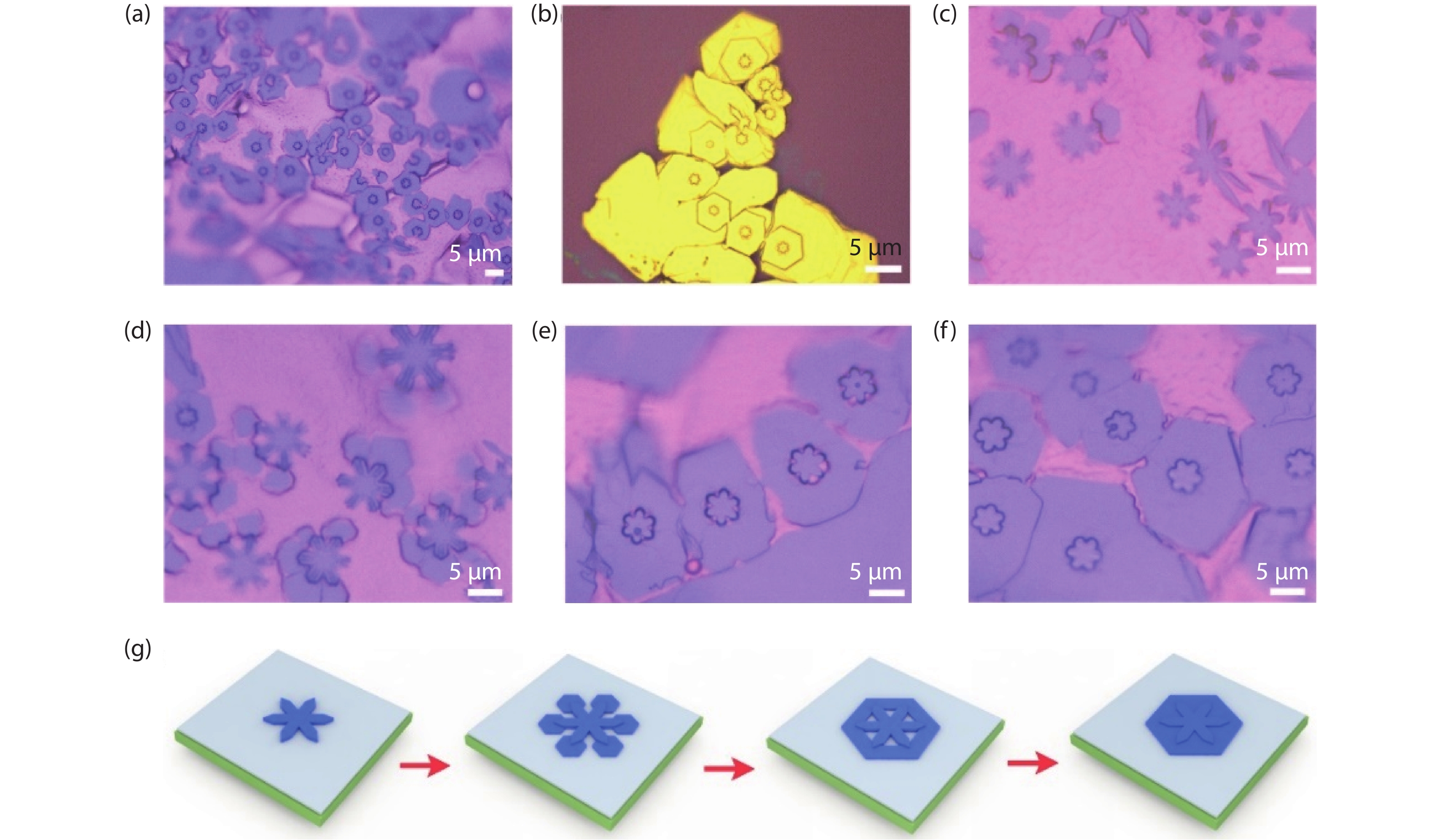
Fig. 4 (Color online) Growth of novel Mo2C pyramid structures. (a) Optical images of the large-area as-grown Mo2C structures on liquid Cu surface and transferred onto SiO2/Si substrate, respectively. (b) AFM image of the single structure, displaying clear layered feature. The inset shows height profile of the structure, showing step feature across the whole flake reflected in thickness. (c–f) Optical images of the growth process of Mo2C structures, showing the time-dependent feature. (g) Schematic diagram illustrates the growth of novel layered Mo2C structures, corresponding to the observations in (c–f).
Download figure:
Standard imageDuring growth process of the novel structures, middle stages are detected (Figs. 4(c)–4(f)). At the initial stage, the nuclei of Mo2C gradually expand, following a diffusion-limited rule under the poor concentration of carbon atoms, and thus lead to star-shaped flakes (Fig. 4(c)). With a continuous feed of carbon source, the carbon atoms are preferably attached onto the font of star-shaped flake, whereas the much higher energy of these sites allow favorable deposition of carbon atoms (Figs. 4(d) and 4(e)). After that, the second nucleation happens, obeying concentration-limited rule, and then results in anisotropic growth with hexagonal shape. It is worth noting that the second growth at the six fonts of the star-shaped flakes is not simultaneous, whereas the structures with one, two, three, four, five and six fonts are all occasionally observed (Fig. S4(b)). Further, the as-grown hexagonal parts of the original flake start to approach with each other and finally emerge into compact flake, while still keeping the hexagonal profile (Fig. 4(f)). The whole process is correspondingly schemed in Fig. 4(g). The direct observation of the intermediates of star-shape centered structures strongly supports the aforementioned inside-out growth mechanism. Further, the intermediates of hexagonal-center Mo2C pyramid structures have also been found (Fig. S5), suggesting a generality of the proposed growth mode.
To further characterize the hexagonal pyramid-like Mo2C structure, aberration corrected scanning transmission electron microscopy annular dark field (STEM-ADF) imaging have been performed, as shown in Fig. 5. A typical STEM-ADF image of the inter-edge region between the two layers of pyramid Mo2C structures is clearly depicted in Fig. 5(a), where a distinct step structure is observed. It is seen that the two layers show uniform thickness, respectively, while displaying an obvious step structure at the middle region, reflected by the different Z contrast. Geometric phase analysis (GPA) is further applied to analyze the level of strain associated with the grain boundaries[20]. A symmetric strain matrix series (Ɛxx, Ɛxy, Ɛyy and rotationxy) is used to map the strain fields and the results are given in the sub-panel in Fig. 5(b). Apparently, the contrast between the two layers is evident. No strain is detected in the two single parts and both of them preserve extremely high crystallinity. Step edges have been imaged and these are atomically sharp. Therefore, it can be concluded that in the growth of the pyramid Mo2C structures, the crystallinity, homogeneity and uniformity of each layer are strictly kept. On the basis, the step-like feature of the pyramid structure is confirmed.
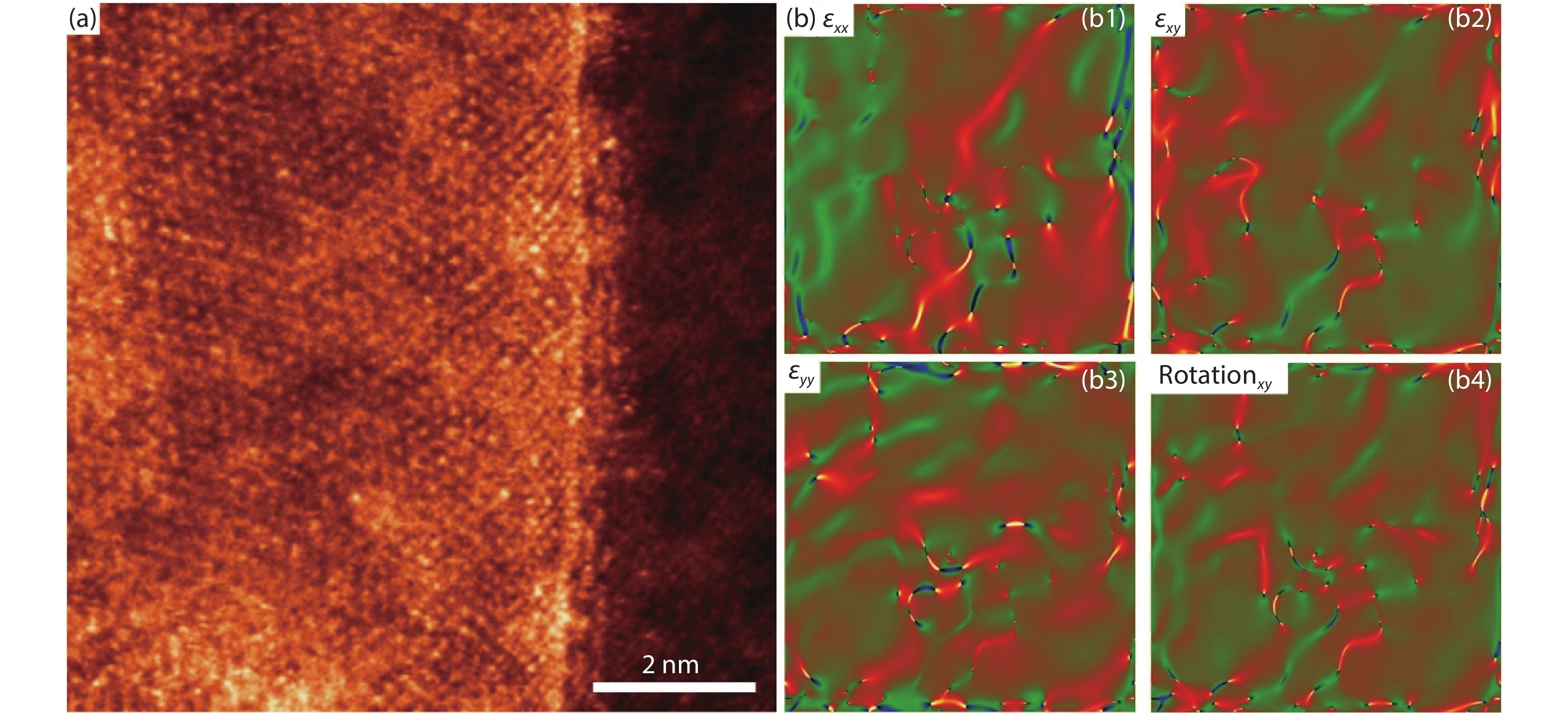
Fig. 5 (Color online) STEM characterization of Mo2C pyramid. (a) STEM-ADF image of a typical edge region in the Mo2C pyramids structures. (b) Strain field mapping based on the image shown in (a).
Download figure:
Standard image4. Conclusion
To sum up, novel Mo2C pyramid structure has been prepared, whereas the vertical spatial control is also realized. The formation of the terraces within the structures arises from the supersaturation-induced center nucleation and concentration-gradient driven diffused growth of a new Mo2C layer on the edge and along with the previous one. Direct observation of the whole evolution process has been demonstrated, further suggesting the in-out growth mechanism for the structures. The controlled synthesis of highly symmetrical pyramid Mo2C structures offer impetus for the design of new 3D spatial structures of other 2D materials.
Acknowledgements
This work was supported by Peiyang Talents Project of Tianjin University (201920701321016), Independent Innovation Fund of Tianjin University (20190903067036)