

Abstract
As spintronic devices become more and more prevalent, the desire to find Pt-free materials with large spin Hall effects is increasing. Previously it was shown that β-W, the metastable A15 structured variant of pure W, has charge-spin conversion efficiencies on par with Pt, and it was predicted that β-W/Ta alloys should be even more efficient. Here we demonstrate the enhancement of the spin Hall ratio (SHR) in A15-phase β-W films doped with Ta (W4−xTax where x = 0.34 ± 0.06) deposited at room temperature using DC magnetron co-sputtering. In close agreement with theoretical predictions, we find that the SHR of the doped films was ∼9% larger than pure β-W films. We also found that the SHR's in devices with Co2Fe6B2 were nearly twice as large as the SHR's in devices with Co4Fe4B2. This work shows that by optimizing deposition parameters and substrates, the fabrication of the optimum W3Ta alloy should be feasible, opening the door to commercially viable, Pt-free, spintronic devices.
Export citation and abstract BibTeX RIS

Original content from this work may be used under the terms of the Creative Commons Attribution 4.0 license. Any further distribution of this work must maintain attribution to the author(s) and the title of the work, journal citation and DOI.
1. Introduction/Background
Recently, the spin Hall effect (SHE) has received a great deal of attention not only from a fundamental physics perspective but also for technological applications in the area of memories, logic and sensors [1, 2]. The SHE is the conversion of a longitudinal current density into a transverse spin current density, which is characterized by the spin Hall ratio (SHR), θSH = JS/JC and materials with large SHRs are desired for spintronic applications. Note that SHR and SHA (spin Hall angle) have been used interchangeably in literature, however the SHA is rigorously defined as the tan−1(JS/JC). Previous studies have demonstrated only a handful of materials that can be sputter-deposited and which exhibit large SHRs at room temperature: these include Pt/doped Pt [3], β-Ta [4], β-W [5] and oxygen doped β-W [6]. There is a technological desire toward Pt-free spintronics and among these candidates, β-W and oxygen doped β-W, have the highest resistance (resulting in larger power requirements) but also show the largest SHR, which is approximately −0.35 and −0.5, respectively [5–8]. β-W is a metastable phase of W that exhibits the cubic A15 structure (SG# 223, Pm-3n) which has two distinct crystallographic sites with two atoms located on each face of the cubic cell. The α-W phase, on the other hand, is the most stable form of W that crystallizes in body centered cubic structure, while exhibiting a smaller SHE [9–12].
There are two categories of mechanisms which govern the SHE: extrinsic and intrinsic. The former arises from spinful electron scattering from impurities or defects typically due to spin–orbit coupling (SOC), while in the latter case the electron is deflected during its transport in-between scattering events [13–15]. This occurs due to presence of spin Berry curvature generated by, for example, SOC-gapped Dirac points in the material's electronic structure [16]. Materials with large intrinsic SHEs are becoming popular as the spin current generating layer of spintronic devices because recently, using concepts form topological physics, a series of sputter-able, low-cost, and giant SHE alloys have been predicted [16]. Among these, W4−xTax at x = 1 was predicted to host the highest spin hall conductivity (SHC); approximately 20% more than pure β-W [16, 17].
Here we experimentally demonstrate that W4−xTax, where x = 0.34 ± 0.06 can be stabilized in the A15 structure on sapphire substrates via room temperature co-sputtering. Using spin-torque ferromagnetic resonance (ST-FMR), we further show that the W4−xTax films host higher SHRs than their doped counter parts (∼9%), in accordance with theoretical calculations [16, 17]. In addition, we found a significant dependence on the type of CoFeB (4:4:2 vs 2:6:2) magnetic layer used; a 2x fold enhancement in the measured SHR for both the pure W and the Ta-doped films when using the 2:6:2 CoFeB composition (with respect to 4:4:2). Future studies on these W3Ta alloys on low-cost SiO2 substrates will open the door to facile device fabrication of Pt-free spintronic devices.
2. Methods, results and discussion
We deposited the pure β-W and W4−xTax film stacks by DC magnetron co-sputtering on Al2O3 substrates at room temperature. The base pressure of the chamber before the deposition was ∼10−9 Torr: the Ar sputtering pressure during deposition was 3 mTorr. Prior to deposition, the substrates were cleaned by a standard multi-step wet cleaning method [18] with an additional annealing step (annealed at 1200 °C for 4 h in atmospheric conditions). In order to get homogeneous film thickness, the substrate holder was rotated at 10 rpm. Pure β-W and W4−xTax films were deposited using sputtering powers of 160 watt (W) and 10 watt (Ta), yielding deposition rates of 5.6 nm min−1 for the β-W films and 6 nm min−1 for the W4−xTax films. Two different compositions of magnetic layers (i.e. Co4Fe4B2 and Co2Fe6B2) were used while keeping their thickness constant at 3 nm. Highly resistive TaN (2 nm) was deposited as a capping layer to prevent oxidation of the active layers. The complete stacks for SHR measurements were W(15)/Co4Fe4B2(3)/TaN(2) (denoted as S1) and W4−xTax(15)/Co4Fe4B2(3)/TaN(2) (denoted as S2), and also W(15)/Co2Fe6B2(3)/TaN(2) (denoted as S3) and W4−xTax(15)/Co2Fe6B2(3)/TaN(2) (denoted as S4), where the number in parentheses is the film thickness in nm of that particular layer.
X-ray diffraction was used to confirm the A15 phase of the film. The diffraction peaks, (200) and (211) indicate that the β-W phase was successfully grown in the A15 crystal structure as shown in figure 1(a). Note that no extra peaks indicating Ta ordering and supercell formation, are visible, implying Ta/W solid solution formation. X-ray photoelectron spectroscopy (XPS) chemical identification and depth profiling was used to determine the composition of W4−xTax films as shown in figure 1(b), where the W peaks match extremely well with bulk metallic W while the Ta peaks are slightly upshifted from bulk metallic Ta. The Ta doping is approximately 8.5 ± 1.5% (x = 0.34 ± 0.06). Ideally, W3Ta should be fabricable, however we were unable to achieve such high concentration of Ta while maintaining the A15 structure. Higher temperature as well as lower power deposition were found to promote the α-phase; using different substrates may be able to stabilize higher Ta-doping concentrations in the A15 phase. The elemental composition of the W4−xTax films was tuned by sputtering power of W and Ta targets. The effective magnetization Meff is extracted by using the Kittel relation [19] as shown in figure 1(c). The saturation magnetization (Ms), measured by vibrating sample magnetometry, and the resistivity (four-point probe method) was 893 emu cm−3 and ρ ≈ 420 μΩ cm, respectively for Co4Fe4B2. For the Co2Fe6B2 samples, these values were 970 emu cm−3 and ρ ≈ 272 μΩ cm. The resistivity of the W films was ρ ≈ 220 μΩ cm and W4−xTax was in the range of ρ ≈ 235–310 μΩ cm.
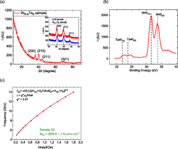
Figure 1. (a) X-ray diffraction patterns for W4−xTax thin film deposited at room temperature, Bragg peaks are labeled with corresponding diffraction planes. Inset: show the β-W and W4−xTax thin films diffraction patterns in short angle range near the peaks. (b) XPS spectra shows the atomic composition of W4−xTax thin film, black dotted lines indicate the peak positions for the bulk W and Ta metals. (c) Resonance frequency as a function of bias magnetic field, the effective magnetization Meff is extracted by using the Kittel relation [19]. Figure (b) y-axis caption should be I (AU) instead of Intensity (AU).
Download figure:
Standard image High-resolution imageThe multilayer stacks were patterned to microstrips with dimensions specially designed for spin-torque resonance experiments (schematic and actual microdevice shown in figures 2(a) and (b)). We employ the ST-FMR method to determine the SHR.
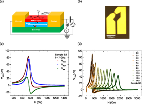
Figure 2. (a) Schematic illustration of a typical ST-FMR measurement arrangement in a bilayer system. (b) Microscopic image of device used for ST-FMR measurements. (c) Typical ST-FMR signal (red dots) of a 10 μm × 10 μm W4−xTax/Co4Fe4B2 device at 7 GHz, fitted to equation (1) (solid black line) with symmetric Lorentzian (Vsym blue curve) and antisymmetric Lorentzian (Vas green curve) components. (d) ST-FMR spectra measured for 5–14 GHz at zero DC bias.
Download figure:
Standard image High-resolution imageIn typical ST-FMR measurements of bilayer systems, several process occur: (1) by the application of a radiofrequency charge current along the film plane, an oscillating transverse spin current is generated in the non-magnetic (β-W or W4−xTax) layer via the inverse spin hall effect. (2) This spin current diffuses along z-direction and, if it is effectively injected into the adjacent magnetic layer (Co4Fe4B2 or Co2Fe6B2), it will exert an oscillating spin torque that influence the magnetization dynamics of the magnetic layer. The magnitude of the spin-torques will thus effect parameters such as lineshape and/or linewidth of the ferromagnetic resonance. (3) A mixing DC voltage, Vmix arises from the oscillating anisotropic magnetoresistance, spin Hall magnetoresistance, and the applied RF current [3, 6, 20, 21], and is thus used to visualize the changes in the ferromagnetic resonance induced by spin-torques. Practically, this is done by measuring Vmix as a function of magnetic field and/or frequency. We applied the magnetic field at 45° (or 135°) to a 10 μm × 10 μm microstrip of the stacks with the DC and RF currents applied though an RF probe and consequently measured the DC response across a bias Tee. The output voltage was then fitted by using equation (1).

Here,  is the DC offset,
  is the coefficient of the symmetric part of the Lorentzian,
  is the coefficient of anti-symmetric part of the Lorentzian,
  is linewidth,
  is the applied external field and
  is resonance field.
Figure 2(c) shows the STFMR signal (red dots are measurement data from W4−xTax/Co4Fe4B2) at 7 GHz with the symmetric Lorentzian (Vsym) and antisymmetric Lorentzian (Vas) components, respectively (extracted from fits to equation (1)). The predominantly symmetric component suggests a high damping-like torque in the magnetic layer [3]. A large amplitude (50 to 100 μV) of the ST-FMR voltage highlights the high quality of the magnetic sensing layer (CoFeB) and enables both a lineshape and linewidth analysis [6] for the calculation of the spin-torque efficiency. We rely here on the linewidth analysis, which directly reflects the amount of generated spin-torque (linewidth broadening) as the charge current is increased through the bilayer. Hence, the ferromagnetic resonance linewidth as a function of DC current Idc for the all samples was fitted at frequencies ranging from 10 to 13 GHz as shown in figures 3(a) and b, and the slope of these plots (δΔH/δIDC) is used to determine the SHR using equation (2).


Figure 3. (a), (b) The FMR linewidth as a function of DC current Idc for the W/Co4Fe4B2 (S1) and W4−xTax/Co4Fe4B2 (S2) bilayers device respectively at f = 10 GHz. (c), (d) For the W/Co2Fe6B2 (S3) and W4−xTax/Co2Fe6B2 (S4) bilayers device respectively at f = 12 GHz.
Download figure:
Standard image High-resolution image
Here,  is SHR (spin-to-charge conversion efficiency),
  is the change in linewidth per unit applied current,
  is the applied frequency,
  is the angle between the current and the applied magnetic field,
  is the effective magnetization,
  is the saturation magnetization,
  is the thickness of the magnetic layer,
  is the resistance of the ferromagnetic layer,
  is the resistance of the metallic layer and
  is the cross sectional area of the device. The effective magnetization (as shown in figure 1(c)) and Gilbert damping coefficients are extracted using the methodology from reference [22] (see supplementary note 1 (available online at https://stacks.iop.org/JPMATER/3/044001/mmedia)) in the magnetic layer from the Kittel dispersion fit of the ST-FMR signal at different frequencies as shown in figure 2(d) and outlined in table 1 for the various film compositions.
Table 1. The spin Hall ratio, Gilbert damping coefficient and effective magnetization extracted by STFMR measurements for all the samples.
| Sample | FM/NM layers | Gilbert damping coefficient α | Effective magnetization Meff (emu cm−3) | Spin Hall ratio |
|---|---|---|---|---|
| S1 | W/Co4Fe4B2 | 0.014 ± 0.001 | 874 ± 1.4 | 0.0118 ± 0.002 |
| S2 | W4−xTax/Co4Fe4B2 | 0.014 ± 0.001 | 858.6 ± 1.5 | 0.0129 ± 0.001 |
| S3 | W/Co2Fe6B2 | 0.012 ± 0.001 | 1019.6 ± 1.2 | 0.0225 ± 0.001 |
| S4 | W4−xTax/Co2Fe6B2 | 0.014 ± 0.001 | 854 ± 1.5 | 0.0240 ± 0.001 |
From analyzing the slopes (figure 3) and equation (2), the SHR of sample S1 is found to be 0.0118 ± 0.002 and for sample S2 is found to be 0.0129 ± 0.001 which is approximately 9% larger than sample S1. Similarly the SHR obtained for sample S3 is 0.0225 ± 0.001 and for sample S4 is 0.0240 ± 0.001 which is approximately 7% larger than sample S3 as shown in table 1 (supplementary figure 1). Our observations are in agreement with previous predictions that A15 phase W4−xTax, where x = 0.34 ± 0.06, with this level of Ta doping, would result in ∼10% increase in the intrinsic SHC and, correspondingly, SHR (due to a negligible change in longitudinal resistivity from Ta doping) [16, 17].
We assume that the source of the SHE in our films is dominantly intrinsic like in pure β-W (due to band structure of the material) rather than extrinsic. This expectation comes from (1) the small amount of doping, (2) the fact that Ta and W are highly miscible and result in W/Ta solid solutions, as implied by XRD and (3) that W and Ta are extremely close in SOC strength. The SOC argument is critical in distinguishing the effects of light dopants (e.g. oxygen or nitrogen) and heavy ones (such as Ta) in β-W films; since extrinsic spin Hall mechanisms depend on defects/dopants causing sudden fluctuations in the local spin-orbit field as an electron travels through the lattice [15], the extrinsic effect of Ta/W substitutional defects is expected to be small compared with O/W doping.
The lower values of SHR obtained in this study compared to previous studies on pure β-W [5] may be explained by interfacial transparency [23]. During the transmission of spin from the nonmagnetic layer to the ferromagnetic layer, spin loss can occur either by spin backflow or spin memory loss due to spin scattering at the interface [24–26]. The film microstructure at the interface can have additional impact on these interfacial effects and the previously mentioned studies were using SiO2 substrates rather than sapphire, as we have. Contribution of these kinds of effects would ultimately underestimate the SHC and SHR values of the spin Hall material. For example, it has been shown that the apparent difference in spin-orbit torque efficiency in Pt/Py films as compared with Pt/Co films can be explained by the spin transparency difference of the interfaces [23]. By factoring in the interface transparency between the ferromagnetic and nonmagnetic layers, the intrinsic SOT efficiency in Pt was determined to be ∼0.3 [24] as opposed to the previously measured value of ∼0.06 [3, 27].
The enhanced value of the SHR for both pure β-W and Ta-doped films when using the Fe-rich Co2Fe6B2 may be ascribed to an interfacial effect; Co-rich and Fe-rich CoFeB layers may have different interfacial energies at the interface adjacent to the nonmagnetic layer as well as TaN capping layer, which contributes to formation of a thin, 'dead' magnetic layer at the interfaces [28–30]. These magnetic dead layers are usually formed by intermixing at the interfaces. Generally speaking, the Fe-rich Co2Fe6B2 is considered a better choice of magnetic layer because of its better perpendicular magnetic anisotropy and tunneling magnetoresistance; both are important characteristics for spintronic devices [31, 32]. It is known that annealing Co4Fe4Co2 and Co2Fe6B2 films at temperatures >150 °C can cause boron diffusion into the neighboring layers [30, 33], however since the films in this study were deposited and processed at room temperature, no significant boron migration is expected. Cross-sectional TEM comparison of β-W films grown using identical deposition conditions on both SiO2 and sapphire substrates with both types of CoFeB layers may be useful in fully understanding these effects.
3. Conclusion
In summary, we have demonstrated the enhancement of the SHR in A15-phase β-W films doped with Ta (W4−xTax where x = 0.34 ± 0.06) deposited at room temperature using DC magnetron co-sputtering. In close agreement with previous theoretical predictions, the SHR of the doped films was ∼9% larger than the pure β-W films. We also found that the SHR's in stacks with Co2Fe6B2 were nearly twice as large as the SHR's in stacks with Co4Fe4B2 which we attribute to spin Hall material and magnetic layer interface transparency. By optimizing the deposition parameters and using different substrates, the ideal W3Ta composition should be achievable and consequently attain the maximum SHR increase up to 20% relative to pure β-W films, paving the way to highly-efficient, commercially viable Pt-free, spintronic devices.
Funding
This research was supported by the Max Planck Institute of Microstructure Physics Halle, Martin Luther University Halle-Wittenberg, the Alexander von Humboldt Foundation and their Sofia Kovalevskaja Award.