


Abstract
A persistent challenge in the field of organic electronics is balancing the optoelectronic properties of π-conjugated semiconducting polymers with their thermomechanical properties. A popular and effective approach to resolve this dichotomy is to blend π-conjugated polymers with amorphous, stretchy elastomers. In this work, poly(diketopyrrolopyrrole-co-thienovinylthiophene) was blended with an easily-prepared poly(dimethylsiloxane)-based phenylurea copolymer (PDMS-PU) to further explore this approach. Interestingly, the differing surface energy and polarity of this soft amorphous copolymer in comparison to other common siloxane-based polymers blended with conjugated polymers showed little impact on the solid-state morphology. Various techniques were used to evaluate the properties of the polymer blends, including atomic force microscopy, UV–vis spectroscopy, and x-ray diffraction. An in-depth morphological evaluation was performed on the blend at varying strain, elucidating the formation of cracks at the nanoscale. The results show a significant decrease in crystallinity and increase in crack onset with increased PDMS-PU content. Fabrication of organic field-effect transistors (OFETs) utilizing the new polymer blends exhibited charge mobility up to 8.2 × 10⁻² cm2 V−1 s−1, and charge transfer characteristics up to 75 wt.% PDMS-PU content. The study shows the promise of PDMS-PU/conjugated polymer blends for use in OFETs, and towards the large-scale preparation of mechanically robust and stretchable electronic devices.
Export citation and abstract BibTeX RIS
1. Introduction
π-Conjugated polymers are an important class of materials with promising application in many novel technologies, including in organic photovoltaics (OPVs), thin films transistors (TFTs), batteries, and thermoelectrics [1–3]. In addition to their good charge transport and narrow bandgap, conjugated polymers are processable through solution deposition and printing which facilitates their use in large-scale production, and creates potential as low-cost alternatives to their inorganic counterparts [4, 5]. Since their discovery, research has been conducted to improve the electronic properties of π-conjugated polymers. Approaches including rational chemical design (backbone and side-chain engineering), and control over the solid-state morphology (solution deposition technique and processing) have been explored extensively [6, 7]. Other important properties such as polymer stability, Siebeck coefficient, and biocompatibility have also been investigated to enable new applications for π-conjugated polymers [8–11]. Mechanical robustness and stretchability have also proven critical in order to develop and expand the utility of semiconducting polymers in stretchable, wearable, and skin-inspired electronics [12–14]. However, mechanical compliance intrinsically competes with charge transport in π-conjugated materials, making the development of stretchable semiconducting polymer challenging [15–17].
Thin films prepared from π-conjugated materials often fail when subjected to tensile strain, due to generation of micro-/nanoscale cracks [18]. Since semiconducting polymer are rigid and crystalline, the polymer network cannot dissipate the tensile energy, which results in crack formation, and ultimately failure of the device [19]. A variety of different strategies have recently been utilized to reduce and control crack propagation upon strain in semiconducting polymers. Rational design of π-conjugated polymer through backbone engineering has shown promise, especially with the inclusion of conjugation-breaking units or non-covalent interactions that contribute to reduce the crystallinity of the polymer and help in energy dissipation, creating 'intrinsically stretchable' materials [20, 21]. However, this approach often requires multi-step synthesis and can negatively impact other properties such as solubility and stability, making it suboptimal for large-scale processing of π-conjugated materials. A new approach based on physical blending of π-conjugated polymers with soft/low-modulus materials has therefore been developed, showing to not only improve the mechanical properties of semiconducting polymers, but also to influence charge transport [22]. Several groups reported promising charge transport characteristics within blends of π-conjugated polymers with polystyrene-block-poly(ethylene-ran-butylene)-block-polystyrene (SEBS), poly(dimethylsiloxane) (PDMS), polyethylene (PE), and others [23–26]. Furthermore, these recent investigations unveiled the importance of the nanoscale solid-state morphology of the polymer blends on charge transport, with continuous networks of nanoconfined semiconducting polymers in the elastomeric matrix being a preferred arrangement [27]. Among the different parameters to impact the solid-state morphology and phase separation, the surface energy of both π-conjugated materials and soft materials was shown to be critical as this parameter influence the polymer miscibility [28, 29]. Unveiling the true nature of the relationship between blend composition and mechanical properties in thin films, and performance in organic electronics is highly desirable, and will yield more efficient and tunable technologies.
Herein, we report the physical blending of a diketopyrrolopyrrole-based (DPP) conjugated polymer with a segmented siloxane-urea copolymer (PDMS-PU) to investigate the effects on electronic and thermomechanical properties (figure 1). The blends prepared contain from 0%–90% wt.% of the soft, amorphous copolymer, and the blends were characterized by UV–Vis spectroscopy, atomic force microscopy (AFM) and x-Ray diffraction (XRD). These new polymer blends were stretched at different strains ( = 0 to 100%) to gain insight into material failure through crack propagation. Complete characterization of the thin film morphology upon strain was performed with optical microscopy, AFM, and XRD. Interestingly, the polymer blends showed no well-defined nanoscale features, in contrast to the typical nanofibrillar phase separated morphology typically observed for polymer blends with PDMS and SEBS, which was attributed to the surface energy of the soft amorphous copolymer, closer to that of the conjugated polymer [23]. Upon strain, blending was shown to significantly reduce crack propagation, going from an average width of 2.5 μm for a pure conjugated polymer to around 800 nm when stretched at = 50%. The same polymer blends were used in the fabrication of organic field-effect transistors (OFETs) in order to evaluate the charge transport properties of the conjugated polymer upon blending. When used as semiconducting materials, polymer blends up to 75 wt.% PDMS-PU led to good average charge mobilities. The results obtained through the evaluation of this new blend system highlight the potential of this approach for the design of stretchable and mechanically robust materials. Moreover, utilizing an elastomer with surface energy closer to that of the conjugated polymer is shown to be a promising strategy to rationally fine-tune the solid-state morphology toward stretchable π-conjugated materials and electronics.
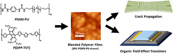
Figure 1. Polymer blending of a segmented siloxane-urea copolymer (PDMS-PU) and semiconducting polymer P(DPPTVT) for reducing crack propagation upon strain, and for the fabrication of organic field-effect transistor devices (OFETs).
Download figure:
Standard image High-resolution image2. Results and discussion
Materials were carefully selected and prepared in order to investigate the impact of physical blending of conjugated polymers with siloxane-based polyurea polymers on electronic and thermomechanical properties. Poly(diketopyrrolopyrrole-co-thienovinylthiophene polymer) (P(DPP-TVT)) was selected as a π-conjugated polymer because it was previously shown to possess favorable mechanical and charge transport properties [30]. This polymer was blended with a segmented siloxane-urea copolymer, namely poly(dimethylsiloxane)-phenylurea (PDMS-PU) copolymer prepared by polyaddition between commercially available aminopropyl-terminated low-molecular weight polydimethylsiloxane and 1,4-phenylene diisocyanate [31, 32]. This soft polymer was chosen as mechanically compliant component in the polymer blends for specific reasons. First, the preparation of the materials is straightforward, and its segmented structure can allow for a careful control on the physical properties, including molecular weight and solubility [33, 34]. Second, silicon-based polymers were shown to lead to phase separation when blended with conjugated polymer, resulting in the confinement of the conjugated polymer chains [23, 35]. It should be noted that the PDMS-PU copolymer has a surface energy different to that of traditional poly(dimethylsiloxane) due to the presence of the polyurea component [36]. This difference was expected to affect polymer miscibility and domain size, ultimately impacting charge transport of the semiconducting composite in organic electronics. Finally, the presence of intermolecular hydrogen bonds between the polymer chain leads to high stretchability, as confirmed by tensile pull testing showing a maximum elongation higher than 125% (figure S1 (available online at stacks.iop.org/FPE/5/035001/mmedia)) [37]. To fully investigate the influence of blending on the mechanical properties of the π-conjugated polymer, different blends were prepared by solution-phase mixing of P(DPPTVT) with 0 to 90 wt.% PDMS-PU.
UV-visible spectroscopy was first used to probe any changes in the optical properties of the π-conjugated polymer upon blending. This technique has previously been used to provide information on molecular aggregation through an analysis of the 0–0 and 0–1 peaks of the donor-acceptor charge transfer band, respectively associated to aggregated and non-aggregated species [38]. To gain insight on the influence on PDMS-PU on molecular aggregation and potential impact on charge transport, the different polymer blends were spin-coated onto silicon wafers (Si/SiO2) to generate thin films that were evaluated before and after a thermal annealing at 150 °C, which mimic the conditions used for the fabrication of thin film transistors. The results are depicted in figures 2(a) and (b). The addition of the PDMS-PU segmented copolymer did not greatly altered the UV–vis spectra of the π-conjugated polymers, and absorption bands attributed to π-π* transitions (λ = 420 nm) and donor-acceptor charge transfer (λ = 800 nm) were observed regardless of the ratio of PDMS-PU added to the blend. Before thermal annealing (figure 2(a)), the intensity of the 0–0 peak, associated with aggregated π-conjugated polymer chains, remains fairly stable upon addition of PDMS-PU, indicated a minimal effect of the soft polymer on molecular aggregation of the conjugated polymer. Interestingly, the thermal annealing treatment at 150 °C (figure 2(b)) caused a more obvious effect on molecular aggregation. In the annealed films, the intensity of the 0–0 absorption peak slightly decreased upon addition of PDMS-PU (up to 50 wt.%) and increased back slightly for the polymer blends at 75 and 90 wt% PDMS-PU. Moreover, the incorporation of PDMS-PU caused a slight blue shift in the absorption band centered around λ = 800 nm. Such hypsochromic shift typically indicates a decrease in molecular aggregation [39]. These results indicate that the addition of PDMS-PU has an impact on molecular aggregation of the conjugated polymer, especially after the thermal annealing treatment.

Figure 2. UV–vis spectra of P(DPPTVT) blended with 0 to 90 wt.% PDMS-PU as cast on Si/SiO2 (thin film) (a) before thermal annealing at 150 °C; (b) after thermal annealing at 150 °C; x-Ray diffraction (XRD) spectra of P(DPPTVT) blended with 0 to 90 wt.% PDMS-PU thin film on Si/SiO2: (c) before, and (d) after thermal annealing at 150 °C.
Download figure:
Standard image High-resolution imagePrior experimentation using x-ray diffraction (XRD) has revealed that blending conjugated polymers with soft polymers tends to significantly impact crystallinity in the solid-state [24]. Therefore, to probe for the influence of the addition of PDMS-PU on film crystallinity, x-Ray diffraction (XRD) was performed directly on thin films of the blends (figures 2(c) and (d)). The conjugated polymer by itself was shown to be largely amorphous, with some crystallinity represented by a peak at 2θ = 4.2° that is typically associated with lamellar stacking of the polymer chain. The addition of increasing proportions of PDMS-PU caused this peak to progressively and completely disappear, indicating a significant decrease in crystallinity. Since thermal annealing is a common treatment to promote crystallinity, XRD was also utilized to evaluate crystallinity after thermal annealing at 150 °C for 30 min. (figure 2(d)). The thermal treatment increased the crystallinity of the conjugated polymer, as confirmed by an important rise in intensity of the lamellar peak. However, the blends with more than 50 wt.% PDMS-PU remained mostly amorphous, which can be attributed to the soft polymer in the thin film preventing lamellar stacking. As described in previous reports, even if semiconducting materials are not highly crystalline and mostly amorphous, the conformational order in aggregates can be enough to allow for a good charge mobility [40, 41]. Based on the results obtained by both UV–vis spectroscopy and XRD, blending of PDMS-PU with the conjugated polymer influences both crystallinity and chain aggregation. As observed in UV–vis spectroscopy, aggregation is related to the amount of PDMS-PU added, but the relationship is not well-defined. Conversely, the crystallinity, observed via XRD, decreases predictably as a greater proportion of elastomer is added. Nonetheless, this nanoscale morphology can enable a percolation pathway for charges to move in the semiconducting polymer phase dispersed in the stretchable matrix.
In order to get insight into the molecular aggregation following blending, the two components' surface energies were calculated by contact angle measurements using a previously reported procedure (table 1) [42]. Surface energy is known to be a critical parameter for controlling phase separation in polymer blends, and gives direct indication on the miscibility of two materials [43]. While other parameters such as the Flory-Huggins parameter are important to get a full picture of polymer blend morphology, surface energy provides important insight on the interaction of PDMS-PU and the semiconducting conjugated polymer [44]. This is also linked to domain purity and size which are important for charge transport. The calculated total surface energy ( ) of PDMS-PU was found to be 25.13 mJ m−2, which in comparison with PDMS (12.54 mJ m−2) is closer to the surface energy of P(DPPTVT) (43 mJ m−2). This trend in surface energy is also observed for the polar and dispersive components of the surface energy
  and
and  . This provides a likely explanation for the difference in molecular aggregation when the conjugated polymer is blended with PDMS-PU versus previously reported examples of conjugated polymer/PDMS blends. Since the surface energy of PDMS-PU is closer to that of P(DPPTVT) than is the surface energy of PDMS, the aggregation of P(DPPTVT) in a matrix of PDMS-PU can be reduced, in comparison to a matrix of PDMS. [27, 45]
Table 1. Contact angle data and surface energy results calculated using Owens–Wendt method.
| Contact angle (°) | Surface Energy (mJ m−2) | ||||
|---|---|---|---|---|---|
| Polymer | H2O | CH2I2 |  |
 |
 |
| P(DPPTVT) | 96.8 | 60.2 | 43.00 | 12.55 | 30.45 |
| PDMS-PU | 105.5 | 77.3 | 25.13 | 5.59 | 19.54 |
| PDMS [36] | 109.5 | 91.4 | 12.54 | 1.49 | 11.05 |
Previously observed in various conjugated polymer and soft elastomer blends, phase separation has an important effect on the thermomechanical and electronic properties of polymer blends. To probe for such phenomenon in P(DPPTVT)/PDMS-PU blends, atomic force microscopy was performed to examine the surface topology of the blends after thermal annealing. Nanoscale topology was evaluated for the 0 to 90 wt.% PDMS-PU/conjugated polymer blends, and the results are summarized on figures 3 and S2. Interestingly, in comparison to previously reported polymer blends with SEBS or PDMS, the new polymer blends did not show the formation of a well-defined nanoscale topology or nanowire-like domains of conjugated polymer upon addition of PDMS-PU [23, 27]. All of the blends showed a relatively smooth surface, but the addition of PDMS-PU to the conjugated polymer, going from 0 to 90 wt.%, increased the root mean square roughness (Rq) of the films. Neat P(DPPTVT) films showed a smooth surface morphology that became more globular upon addition of PDMS-PU, with an overall rougher appearance. For larger content of PDMS-PU (75 and 90 wt%), larger non-defined features were observed, which can be directly attributed to a larger amount of PDMS-PU in the system. It is also important to note that, at 75 and 90 wt.% PDMS-PU, the recording of a good quality image by AFM was found to be particularly challenging as the blends became very soft, even after thermal annealing.
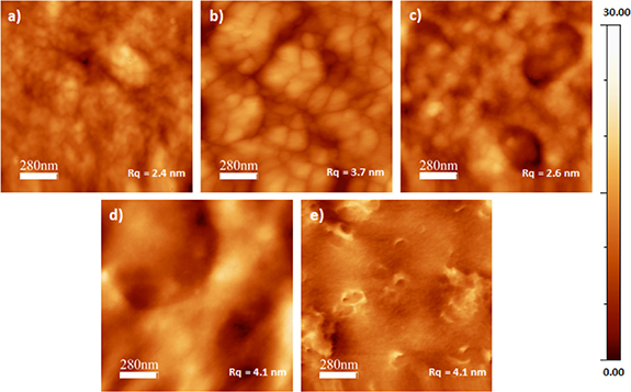
Figure 3. Atomic force microscopy images (height) P(DPPTVT)/PDMS-PU blends containing (a) 0 wt.%; (b) 25 wt.%, (c) 50 wt.%, (d) 75 wt.%, and (e) 90 wt% PDMS-PU after thermal annealing. Scale bar is 280 nm.
Download figure:
Standard image High-resolution imageTo further support the difference between PDMS-PU with common PDMS, blending of P(DPPTVT) was performed at 50 mol% with PDMS (figure S3), which showed the formation of smaller, more well-defined structures resulting from nanophase separation between the conjugated polymer and the siloxane-based polymer. This important difference can be attributed to the surface energy of the PDMS-PU which is closer to that of P(DPPTVT), potentially increasing the miscibility of the two matrices. Nonetheless, all polymer blends with PDMS-PU showed a relatively uniform topology at the nanoscale.
Following the initial characterization of the solid-state morphology of the PDMS-PU/conjugated polymer blends, further evaluation of the morphology under strain was performed by AFM using a soft lamination procedure as detailed in the Supporting Information. Thin films were stretched at different percentage elongation (from 0 to 100%) and the resulting films were directly imaged by AFM to probe for crack formation and widths. The results obtained from this investigation are summarized in figures 4, and S4 to S8. This investigation was performed on non-annealed samples as the intermolecular hydrogen bonds enabled in PDMS-PU were shown to have a low tolerance to thermal annealing, thus significantly complicating the soft lamination on various substrates. Despite the progressive addition of PDMS-PU to the conjugated polymer, all samples formed cracks at ∼10% strain. Interestingly, the crack width was shown to progressively decrease upon addition of the soft amorphous copolymer which confirms its plasticizing effect in the blends.

Figure 4. Atomic force microscopy (AFM) height profiles of P(DPPTVT) blended with (a) 10 wt.%; (b) 25 wt.%; (c) 50 wt.%; (d) 75 wt.%, and (e) 90 wt.% of PDMS-PU in thin films stretched at 100% strain elongation. Scale bar is 2 μm.
Download figure:
Standard image High-resolution imageSevere crack propagation was observed in neat P(DPPTVT) films, with crack widths reaching more than 3 μm at 75% strain elongation (figure 5). The presence of PDMS-PU in the films considerably reduced crack propagation under strain, which remained fairly stable upon high strain. Films that contained more than 50 wt.% PDMS-PU exhibited cracks less than 1 μm in width up to 100% strain, which should be attributed to the inclusion of an amorphous materials. PDMS-PU helps dissipate energy in the films upon strain, thus affecting the final crack widths. Crack size reduction occurred in the blended films independently of blending ratio, resulting in uniform distribution of smaller cracks as opposed larger, localized cracks in native P(DPPTVT). In addition to crack width, the area of the cracks generated upon strain was also evaluated (figures 5 and S9 to S13). Similar to the results observed in crack width analysis, the addition of PDMS-PU significantly contributes to reduce the area of the cracks generated upon strain, especially below 50 wt.%. PDMS-PU. The impact of the soft polymer on crack area can also be observed for higher content of PDMS-PU, with crack area going from 30% at 100% elongation for the pure conjugated polymer to less than 10% at 100% elongation for the 50 wt.% PDMS-PU/conjugated polymer blend. This significant impact on crack propagation is particularly promising for the fabrication of wearable or soft electronic, where devices might undergo multiple cycles of strain, ultimately leading to failure from accumulation of large cracks [46]. The energy dissipation observed for blends of P(DPPTVT)/PDMS-PU is promising, as it could postpone or prevent device failure over repeated strain loading.

Figure 5. (left) Thin-film crack size versus the different percent strains at 0–90 wt.% of PDMS-PU copolymer (n = 3) and (right) percent cracked surface area versus strain as determined by atomic force microscopy (AFM), before annealing.
Download figure:
Standard image High-resolution image
Films of P(DPPTVT)/PDMS-PU blends were used to fabricate bottom-gate bottom-contact (BGBC) organic field-effect transistors (OFETs) to evaluate the electronic properties of the system. The procedure for device fabrication is outlined in the Supporting Information. Briefly, the polymers were dissolved in chloroform at a total polymer concentration of 3 mg ml−1 in varying ratios of semiconducting polymer to segmented amorphous polymer (i.e. P(DPPTVT)/PDMS-PU). Following dissolution, the polymer solutions were spin-coated onto octadecyltrichlorosilane treated n+-doped silicon wafers with 300 nm thick SiO2 dielectric pre-patterned with gold as source and drain electrodes. After deposition, the thin films were annealed on a hot plate at 150 °C for 30 min in an N2 filled glovebox, and the fabricated devices were directly evaluated. The results obtained for the characterization of the polymer blends in OFET devices are summarized in table 2. The output characteristic and transfer curve for the different devices are also depicted in figures S14 to S33.
Table 2. Average and maximum hole mobilities (μhave, μhmax), threshold voltages (Vth), and Ion/Ioff for OFETs fabricated from polymer blends of 0, 50 and 90 wt% PDMS-PU before and after thermal annealing. Measures averaged on 5 devices.
| Sample | Annealing Temperature [°C] | W/L | μhave/μhmax [cm2 V−1 s−1] | ION/IOFFave | Vthave [V] |
|---|---|---|---|---|---|
| 0 wt.% PDMS-PU | as cast | 10 | 1.1 ± 0.1 × 10⁻²/1.2 × 10−2 | 103 | −3 |
| 150 | 3.0 ± 0.3 × 10⁻²/3.6 × 10−2 | 104 | −17 | ||
| 25 wt.% PDMS-PU | as cast | 10 | 4.0 ± 2.0 × 10⁻³/1.1 × 10−2 | 103 | −23 |
| 150 | 4.0 ± 1.0 × 10⁻²/8.2 × 10−2 | 104 | −12 | ||
| 50 wt.% PDMS-PU | as cast | 10 | 4.0 ± 1.5 × 10⁻⁴/1.0 × 10−3 | 102 | −17 |
| 150 | 2.3 ± 0.5 × 10⁻²/3.6 × 10−2 | 104 | −14 | ||
| 75 wt.% PDMS-PU | as cast | 10 | 6.0 ± 3.0 × 10⁻⁴/1.9 × 10−3 | 102 | −32 |
| 150 | 2.0 ± 0.2 × 10⁻²/2.4 × 10−2 | 104 | −17 | ||
| 90 wt.% PDMS-PU | as cast | 10 | 3.1 ± 0.1 × 10⁻⁶/7.0 × 10−6 | 101 | −46 |
| 150 | 2.8 ± 0.4 × 10⁻⁶/3.8 × 10−6 | 101 | −4 |
Thin film transistor devices fabricated with 0, 25, 50, 75, and 90 wt.% PDMS-PU/conjugated polymer blends all exhibited transistor-like behaviour. Although bottom-gate top-contact (BGTC) architecture is known to minimize the contact resistance and improve mobility, a BGBC architecture was used due to its ease of fabrication (pre-patterned substrate) and compatibility with large-scale device fabrication (minimal exposure of the device components to solvents and chemicals) [47]. Devices prepared from P(DPPTVT), i.e. 0 wt.% PDMS-PU, showed an average mobility of 0.0011 cm2 V−1 s−1, which was increased to 0.030 cm2 V−1 s−1 upon thermal annealing. It is important to mention that, as commonly observed, thermal annealing of the sample led to improved device characteristics and charge mobility [48, 49]. Moreover, despite being lower than typical mobility values obtain for top-contact devices, this result is comparable with previously reported charge mobility obtained using similar device architecture [50, 51]. Interestingly, the addition of PDMS-PU did not significantly affect charge mobility, going from 0.030 cm2 V−1 s−1 for the non-blended conjugated polymer to 0.040 cm2 V−1 s−1 and 0.023 cm2 V−1 s−1 for the 25 and 50 wt.% PDMS-PU blends respectively, after thermal annealing. Upon further addition of PDMS-PU to 75 wt.%, a charge mobility of 0.020 cm2 V−1 s−1 was observed, which is similar to the non-blended polymer. This result was also rather surprising as the 75 wt.% PDMS-PU blend was shown to have a low crystallinity, as confirmed by x-Ray diffraction. Despite the fact that the mechanical properties of the polymer blends are measured on non-annealed thin films while optimal electronic performance are being observed after thermal treatment, this result indicates that not only PDMS-PU can act as a plasticizer improving the mechanical properties of the conjugated polymers, but the phase separation induced by the physical blending can also help maintaining good charge transport in devices even when 75 wt.% of PDMS-PU is used in the polymer blend. Upon addition of 90 wt.% PDMS-PU, charge mobility drastically decreased to 2.8 × 10⁻⁵ cm2 V−1 s−1. This reduction in performance was attributed to the decreased amount of P(DPPTVT) in the device channels. Throughout the addition of PDMS-PU and evaluation of the performance in OFET devices, changes in device performance can be observed in both the transfer and output curves. Poorer performance with respect to the appearance of the output curves is attributed to an increased contact resistance as the amount of PDMS-PU was increased in the blends. Despite not leading to an increase in charge mobility in comparison to other previously reported system, the addition of PDMS-PU is an effective strategy to control crack propagation and diminish potential device failure upon mechanical stress. Therefore, the results obtained from device fabrication show promise for the large-scale fabrication of electronic devices, mostly due to the minimal optimization required for BGBC devices, with decent charge mobility and on/off current ratios for the polymer blends.
3. Conclusion
In summary, the physical blending of a semiconducting polymer, P(DPPTVT), with a PDMS-based polyurea copolymer (PDMS-PU) in ratios from 0 to 90 wt.% PDMS-PU was performed and the thermomechanical and electronic properties of the resulting materials were evaluated. UV–vis spectroscopy showed that the inclusion of the soft polymer to the conjugated polymer can affect molecular aggregation. XRD was used to probe the crystallinity of the polymer blends, which showed that crystallinity decreased significantly in blends containing above 50 wt.% PDMS-PU. The new polymer blends were shown to suffer from nanoscale crack formation when strained between 10 and 100% elongation, attributed to the dissipation of the tensile energy upon mechanical stress. However, the addition of PDMS-PU to the conjugated polymer significantly influenced the crack propagation (crack widths and areas), which were shown to be considerably reduced in the polymer blends. This important effect was a direct result of the soft amorphous copolymer reducing crystallinity, and helping the film to accommodate strain through energy dissipation. Finally, the electronic properties of the polymer blends were evaluated by the fabrication of organic field-effect transistor devices. Importantly, charge mobility and ION/IOFF for devices built with the polymer blends were comparable to those built on neat P(DPPTVT), maintaining an average hole mobility of 0.020 cm2 V−1 s−1 even when 75 wt.% PDMS-PU was added in the polymer blend. Together with the results obtained from crack propagation analysis upon strain, the measured electronic properties confirm PDMS-PU as an appropriate amorphous additive to generate softer and mechanically robust blends with conjugated polymers. Given the ease of preparation and reduced content of semiconducting polymer needed, these new active blends show potential for the large-scale fabrication of new soft electronic devices with enhanced durability and good performance.
Acknowledgments
The authors thank Tricia B. Carmichael and her group (U. Windsor) for help with materials characterization. J P thank the Government of Ontario for financial support through an Ontario Graduate Scholarship. M U O thanks NSERC for a doctoral scholarship.
Conflicts of interest
The authors declare no conflict of interest.
Author contributions
All authors contributed to the manuscript. All authors have given approval to the final version of the manuscript.
Funding Source
This work was supported by the Natural Sciences and Engineering Research Council of Canada, NSERC (RGPIN-2017- 06611). This work was also supported by the NSERC Green Electronics Network (GreEN) (NETGP 508526-17). The authors declare no competing financial interest.