

Abstract
This work presents a novel architecture, exemplified for electrophysiological applications like ECoG that can be used to detect Epilepsy. The new ECoG is based on a mixed analog-digital architecture (Pulse Amplitude Modulation PAM), that allows the use of thousands of electrodes for recording. Whilst the increased number of electrodes helps to refine the spatial resolution of the medical application, the transmission of the signals from the electrodes to an external analysing device appears to be a bottleneck. To overcoming this, our work presents a hardware architecture and corresponding protocol for a mixed architecture that improves the information density between channels and their signal-to-noise ratio. This is shown by the correlation between the input and the transmitted signals in comparison to a classical digital transmission (Pulse Code Modulation PCM) system. We show in this work that it is possible to transmit the signals of 10 channels with a analog-digital architecture with the same quality of a full digital architecture.
Export citation and abstract BibTeX RIS

Original content from this work may be used under the terms of the Creative Commons Attribution 4.0 licence. Any further distribution of this work must maintain attribution to the author(s) and the title of the work, journal citation and DOI.
1. Introduction
1.1. Brain computer interfaces uses
Brain Computer Interfaces (BCI) promise to improve the diagnoses of some neurological diseases such as Parkinson [1], Alzheimer [2], Epilepsy [3], Tumors [4] and loss of sensomotoric functions in paraplegic patients [5, 6]. Not only does BCI impact the health care industry, there is some engrossing reports where BCI are used in research studies to examine the relationship between theta functions and short-term memory and learning [7].
BCI can be classified based on their invasiveness, for example electroencephalography (EEG), MEG are not invasive, meaning that it does not require surgery to use these BCI, but their spatial and temporal resolution are less than invasive BCI, such as ECoG, Utah [8, 9] proves. In these terms, regarding spatial and temporal resolution, the more invasive the BCI technology used is, the bigger the spatial and temporal resolution increase [10]. The amplitude of the recorded signals follows the same logic, the nearer the electrode is to the neuron, the bigger the amplitude of the recorded signals is, but these signals have a very small amplitude and they need amplification [11]. These signals are characterized to be signals with low frequencies less than <300 Hz and a very low amplitude of <100 μV [12, 13]. As we said before, BCI are very commonly used in clinic to monitor and diagnose neurologic disease like Epilepsy.
1.2. ECoG and local field potentials ECoG
The ECoG can record signals coming from a population of neurons near the cortex, this composition of signals coming from the group of neurons is called Local Field Potential (LFP) [14]. Brains signals coming form the LFP are appropriate for studies of neuronal activity [15]. As such, these signals have been used as a method to diagnose the epilepsy. The first uses of ECoG for the diagnosis of epilepsy were reported in 1935 by Foerster & Altenburger [16, 17]. These signals coming from the LFP can be recorded with ECoG [18]. Moreover there are some studies that show that it is possible to record Actions Potential (AP) [19, 20]. In this case, the electrical characteristics of these signals need to be considered. They have a maximal frequency of 1–6 Khz and an amplitude of less than 500 μV [12]. The system used to record these signals need an amplification of 40–60 db, a bandwidth of the filters of 1–6 KHz and 16 bits [21, 22] and a sampling rate between 1-31.25KS/S [23, 24].
1.3. Uses of ECoG and epilepsy
Clinical ECoG systems use electrode contacts with a diameter between 2–4 mm and inter-electrode distances of 10 mm. Typically the electrodes are made of platinum [25–27] and are placed on the surface of the cortex [28]. Ravat et al [29] studied the potential use of ECoG for the diagnosis and therapy of epilepsy [30] and concluded that the success of an Epileptic surgery depends on the accurate localization and removal of the epileptogenic tissue [29]. Rosenow defined the epileptogenic zone as the area of the cortex indispensable for the generation of clinical seizures [31]. It has been shown that it is not always possible to treat epilepsy with drugs, instead epileptic surgery is used [32]. The epileptic focus can be determined with ECoG [33–35] by mapping [36] the recorded signals. The signals can be classified into direct current (DC) and high frequency oscillations (HFO). The DC frequency range is defined between 0.016–1 Hz and the HFO is defined as the frequency range across the high gamma signal, this corresponds to ripples (80–200 Hz) and fast ripples (250–500 Hz). These signals allow one to delineate the epileptogenic area [37, 38].
It has been shown that higher spatial resolution can be obtained by increasing the number of electrodes [39–41] to improve the diagnosis of epilepsy [42]. For this reason, we propose an electronic architecture that increases the number of electrodes in an ECoG while reducing the number of wires decreasing the associated electrical and mechanical problems [43]. Moreover, smaller electrodes can be used to record the APs from the brain cortex [19].
Normally, increasing the number of contacts causes a corresponding increase in the number of wires that connect to the electrodes. Consequently, larger plugs are needed in order to connect the ECoG making the labor of the physicians ECoG more difficult. Moreover, this leads to an increased risk of infection and mechanical failure. This mechanical failure can produce electrolysis, due to the exposure of the wires and the circulating a current, in case that stimulation is applied [44]. Additionally it has been suggested that an increased number of cables has an effect of cross talk at the connector [45]. For these reasons, it is desirable to reduce the amount of wires used to connect the ECoG with an external device.
The goal of this work is to develop a new electronic architecture that can be integrated into the ECoG that would increase the number of contacts while reducing the number of wires, through the use of multiplexing techniques, and at the same time reducing the power consumption of this electronic architecture. This way, it would be possible to keep an array flexible, reducing the risk of wire failure, and reducing the parasitic capacitance and resistance.
Taking into account the functionalities that this architecture has to stimulate and the requirements to record the signals described avobe.
We compare two possible architectures which will be discussed in the next sections. Some previous studies have shown that an electronic multiplexing system distributed on an ECoG can reduce the amount of wires and maintain the flexibility of the array [43]. Regarding this matter, we would like to show that an analog multiplexing architecture, where the signal coming from the electrodes is analog transmitted, can multiplex more electrodes than a digital equivalent multiplexer system. To support this hypothesis we develop two multiplexing systems, one to transmit the signals coming from the electrodes digitally and the other to transmit the signals analog. The general idea is derived from line scan CCD devices, where analog signals are transmitted in a sequenced, digital-like manner.
Previous works have proposed architectures to record cortical potentials directly from the brain including amplifiers, analog multiplexer and band passfilter + ADC (e.g. 'bio-amplifier') such us open-ephys recording system [46]. However, in this case only the electrodes are implanted in the brain [47], but not the electronics, and therefore it is not suitable for chronic implantation. The Itan [48] (Intan, Los Angeles, California, USA) architecture presents a thermal power density higher than 40 mW cm−2 which is above the limit allowed to conduct cortical recordings. The goal of this study is to demonstrate that the proposed mixed architecture offers advantages in terms of bandwidth transmitted while maintaining the same quality of the ECoG recordings and keeping a power density below the minimum for chronic implantable use.
2. Materials
2.1. Proposed multiplexing system
2.1.1. Digital multiplexing system
A digital multiplexing system can be conceived as an architecture in which small chips contain electrodes connected through a bus in order to transmit the digitized signals using a similar data transmission protocol as the token bus standard IEEE 802.4 [49, 50]. Here, the chips transmit data sequentially after an external device sends a token signal to the bus and the chips start to transmit. Figure 1 contains a diagram of this transmission protocol.

Figure 1. Considerations, ECoG for 1002 contacts (167x6) with distributed digital multiplexer. Simplified model.
Download figure:
Standard image High-resolution image2.1.2. Analog multiplexing system
This architecture uses digital signals to control the system and to transmit the analog data. These systems are called mixed system. They are not new. Some works have been proposed in this direction [51, 52]. The architecture is based on the concept of eGrains, where tiny and independent chips communicate with each other to complete a task together [53]. Our concept is based on many electronic chips spread over the ECoG working together to multiplex the brain signals. To build this architecture, we divide the architecture into blocks and cells. The cells are units composed of one microcontroller (μC) that control 6 CMOS switches. 6 arrays of cells with an amplifier are used to amplify the signals coming from the electrodes forming a block. For this reason, 167 chips are required to multiplex 1002 electrodes. The system has been designed such that it can be controlled by 8 wires for each block (1 clock, 1 stimulate, 1 record wire, 2 serial, and 3 power wires).
Figure 2 represents the signal pathways to record the brains signals from 12 electrodes and the pathway used to control the array configuration.
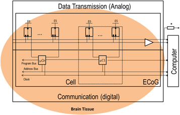
Figure 2. ECoG, Distributed mixed signal architecture, simplified model. * line can be used for stimulation. The microcontrollers only control the CMOS switches connecting a selected electrode with the recording line.
Download figure:
Standard image High-resolution imageThe architecture is designed such that the amplifier is implanted on the ECoG. This study, however, focuses on the data transmission for the digital and mixed architecture. Moreover, it is important to consider that for the mixed architecture it is possible to connect a larger amount of electrodes to an amplifier than with the digital system in which the use of one amplifier for each electrode is required. Our hypothesis is that it could be possible to multiplex more electrodes with mixed signal architecture comparied to the equivalent digital architecture described before.
2.2. Register organization for the digital and mixed architecture
2.2.1. Digital architecture
In this architecture the signals are digitally transmitted between the computer and the microcontrollers (μCn) and vice versa (figure 3). In figure 3, the Data, Address and Program lines are used as follows: (1) Data line: Transmits the token and the clock and receives data from the electrodes; (2) Address line: Transmits the sequence in which it will be recorded from the corresponding electrodes; (3) Program line: Sends a programming number for each μC.

Figure 3. Block diagram of the digital architecture with the internal register design. Arows indicate the signal pathway.
Download figure:
Standard image High-resolution imageThe internal register organization can be summarized as follows: First the μCs have the same base program (with the register sequence), since it is not practical to make a specific program for each μC. The program stores an address in a program register (PR) that is used to identify the μC 'n' from which it will be recorded or stimulated. Second, the program stores another address (AR) to identify the recording electrode (E1...E6) corresponding to that μC 'n' from which it will be recorded. This address register is stored sequentially through a first-in first-out (FIFO) stack (AR0...AR9). Based on this configuration sequence, the μCs start to record from the electrodes E0...E5. This routine is executed by an external signal called 'Token' which is transmitted through the Clock/Data line (see figure 3 bottom) connected in parallel to all the microcontrollers (μCn). These recorded signals are then transmitted through the bidirectional Clock/Data line to the external device (computer).
Here it is important to highlight that for this system to work the signals have to be amplified before they enter the microcontroller.
2.2.2. Mixed architecture (analog and digital)
The architecture design consists of two pathways, the analog pathway used for recording or stimulating, and the digital pathway used to program, control and reconfigure the electrode array (figure 4).
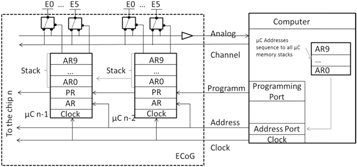
Figure 4. Distributed mixed signal architecture internal register design, block diagram.
Download figure:
Standard image High-resolution imageThis electronic architecture integrates CMOS switches on each electrode. The CMOS switches are used to connect the electrode with the recording pathway or the stimulating pathway. In the recording pathway, the recorded analog signals are amplified and transmitted analogically.
The memory organization is very similar to the digital architecture, but here the data from the electrodes E0...E5 is analog, and is consequently transmitted analogically through a CMOS. On the other hand, signals can be transmitted analogically through the CMOS switch for stimulation. The internal register sequence is executed through an external Clock pulse instead of using a bit sequence. This can be done because there is no more need to transmit a digital value through the system's 'data' line. The Clock is now the only signal in this bus and for this reason this line can be renamed as the Clock line. The other registers, including the PR and the AR, as well as their functionalities are the same as in the digital architecture. This architecture is called mixed architecture, because the control and the configuration of the architecture is digital but the data is analog.
In this case, compared to the previous architecture, the number of amplifiers needed is less because the electrodes are temporally connected directly to the output amplifier. In this way, the number of amplifiers is drastically reduced and the power consumption needed for the system is also likewise reduced.
2.3. Architecture functionalities
2.3.1. Microcontrollers initialization and sequence programming, FIFO Stack for the mixed and digital architectures
In both architectures the PR with the identification number is programmed the first time the system is powered-up. The PR is a shift register transmitted to the next μC when new serial data (coming from the programming port of the computer) arrives from the program signal.
The address port of the computer sends the instructions to be executed by the μCs. These instructions are transmitted to all μCs into the AR register. These instructions are saved and sequentially listed in the address register memory (stack) of the μCs.
We developed a protocol that writes in the stack of the μCs. This protocol sends a data stream (packet) to the μCs through the address signal.
In this communication protocol, the computer sends a stream containing the information about which μC will be selected using the identifiers C0, C1... Cn. for the microcontrollers μC0 and μC1... μCn. The corresponding μC sends back an acknowledge (AK) byte to the computer. Next, the computer sends another byte to indicate if the chip has to record from or stimulate an electrode (E0, E2, ..., E5). This process is repeated to program another μC (figure 5).
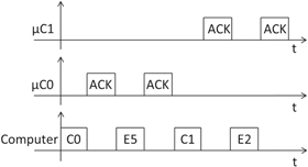
Figure 5. Programing packet sequence. AK: acknowledge, C0, C1: identifiers for selection of μC0 and μC1 and presetting to record from electrodes 5 and 2, respectively.
Download figure:
Standard image High-resolution imageThe non-selected μCs detect that the stream does not contain any message for them and write a no-operation 'NOP' in their stack memory and wait until the communication between the selected μC and the computer has ended.
This process ensures that only one μC is reading from an electrode at any one time. Moreover, this process can be used to identify if a μC is failing when the AK is not received. In that case, it would be possible to reconfigure the array of electrodes without the failing μC or report the failures to the external device. The described protocol gives large robustness in terms of information saved into the μC's memory, as the sequence is verified during the communication and it ensures that the same sequence is saved in all μC without errors.
2.3.2. Microcontrollers reading process
In the digital architecture, a digital token (termed token) is transmitted to the bus by the computer to inform the μCs that it can read its stack memory and then to start recording from the corresponding electrode. When the record is finished, this digital value is transmitted though the Clock/Data bus.
In the mixed architecture, a CMOS switch is used to connect an electrode to the stimulate or to the record pathway. The reading process starts by accessing an internal sequence in the μCs and executing it by an external signal (Clock). This sequence contains the information to record from or to stimulate an electrode. In this work, we only conducted tests to assess the recording pathway of the architecture.
2.3.3. Data transmission
In the mixed architecture, signals are transmitted through Pulse Amplitude Modulation (PAM) [54]. In the digital architecture, the information is digitally encoded and then transmitted serially through Pulse Code Modulation (PCM) [54]. This work compares the PAM and the PCM data transmission rate using the corresponding architectures for an ECoG multiplexer.
To compare how many electrodes could be multiplexed with the digital and the mixed architecture, we used the same hardware including the same μCs. To make this comparison, we considered that the digital system has an analog digital converter (ADC) of 10 bits, which will be serially transmitted. For the mixed system, the data have amplitude proportional to the amplitude of the input signal but the data transmission time is a priory unknown. This can be determined by comparing the PCM and the PAM data transmission time, denoted as tpam and tpcm, respectively.
Let us consider a function A(t) representing a signal recorded by an electrode as the input signal in our system (figure 6). This signal for the digital architecture is sampled, quantified and transmitted serially to an external device (e.g. a PC or another microcontroller) through the data port of the digital system. This process is repeated every Ts period time as it is showed in the figure 6.

Figure 6. The same analog signal A(t) with sampling.
Download figure:
Standard image High-resolution imageThe data transmission starts with a token signal (T) coming from an external device. Next, the microcontroller samples the signal and transmits the digital data (AD0, AD1). The transmitted sequence is finished with a byte to indicate end of the stream (FF). This stream of data is displayed in figure 7:
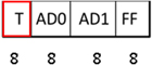
Figure 7. Digital stream for the digital architecture. The token signal (T) is highlighted in red because it is coming from an external device. 8 bits from the token, 10 bits from the analog digital converter and 8 bits to indicate the end of the stream.
Download figure:
Standard image High-resolution imageFor the mixed architecture, the method to transmit the data to an external device is different. In this case, the external device starts with an external pulse signal (P) (red line in figure 8), equivalent to the token signal T in the digital architecture. With the rising edge of P, the input signal A(t) is sampled with a pulse duration tpam with sampled period Ts (figure 8) for its transmission to an external device.

Figure 8. Sampling signal interval of A(t).
Download figure:
Standard image High-resolution imageThis sampling time tpam is for the mixed architecture unknown (figure 9). Note that this time corresponds to the time required to transmit the 10 bits in the digital architecture, and that this time is known for a fixed rate.
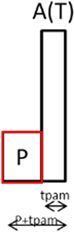
Figure 9. P is the pulse from the external device. Recording pulse in the mix architecture.
Download figure:
Standard image High-resolution imageNext, we estimate tpam in relation to the time required to transmit the digital stream AD0, AD1 of the input signal A(t) in the digital architecture (tpcm) as illustrated in figure 10.

Figure 10. Comparison between the digital data and the analog data transmission time. 8 bits from the token, 10 bits from the analog digital converter and 8 bits to indicate the end of the stream.
Download figure:
Standard image High-resolution imageThis comparison can be done by comparing the bandwidth of each signal. The sampled signal is transmitted through a channel with bandwidth Bc. This limited bandwidth relates to the transmission data rate through the upper transmission limit defined by Nyquist [55, 56]:

where, Dr is the bit rate of the transmitted signal.
On the other hand, the bandwidth of a PAM (BPAM) signal is given by the expression:

A parameter used to characterize the PAM signal transmission is the duty cycle (d), which is defined as the relation between tPAM and Ts:

Replacing (3) with (2) we have:

Defining Fs = 1/Ts, it is possible to rewrite equation (4) as:

According to the Nyquist sampling theorem [57], to avoid aliasing effects it is necessary to sample the signal at least at double its maximum frequency  Replacing this theorem in equation (5) we obtain:

The data rate (Dr) of the PAM signal ( ) is the bandwidth of the PAM signal
  using equations (1) and (6):

On the other hand, for the PCM signal the bandwidth is given by the number of Bits of the quantizer (Q) and the sampling frequency as follows:

According to the sampling theorem of Nyquist, it is possible to write:

Replacing (9) with (1) the respective data rate for PCM is:

Replacing (10) with (7), we obtain the following corollary:
Which is equivalent to:

This corollary remarks the following aspects:
- If the quantization levels of a PCM signal increase, the required data rate to transmit the signal also increases. However the data rate required to transmit the PAM signal is reduced.
- If the PAM signal is constructed with a very small
 (i. e. is very small compared to ), the data rate required to transmit a signal with PAM is greater than with PCM. For example, for a fixed pulse duration if is reduced increases and makes the transmission through PAM less efficient.


These two aspects are proven and tested through an electronic implementation.
2.3.3.1. Metastability and signal resolution
The calculations of the bit resolution of our system will be done in terms of metastability of analog digital converters [58]. The conversion time is due to the settling of the input signal or mismatching [59]. This time is termed metastability. The sampled signal (at the analog input) is assigned a digital value at the analog digital converter. This converter assigns a value to the analog sample comparing this sample with a value in the intern voltage divisor. The settling time can be approximated by a time constant τ of an RC circuit (see table 2.85. pp. 110 in 57). In this table, it is shown that 6 bit resolution requires 4.16 · τ, 12 bits require 8.32 · τ and 20 bits require 13.86 · τ. This table can be described using equation (13):

where k is the number of time constants. A very similar equation is given by Lowsma, for digital analog converters [60].
In our multiplexer circuit we have to consider all time constants τ before the analog digital converter, because they will contribute to the settling time of the digitized signal (see figure 11), and the time constant of this circuit will contribute to the time constant of the analog digital converter. Then it is also possible to calculate the bit resolution of this multiplexer using equation (13).

Figure 11. Schematic of the electronic de-multiplexer architecture for data transmission of elctrophysiological recordings. In the following experimemts we consider this model of parasitic elements arrangement for transmission of pre-recorded real signals.
Download figure:
Standard image High-resolution imageNote that these electrodes are not part of our proposed architecture, but these values should be considered in the calculation of τ. In our computations, we omit them because the impedance of the electrode depends on the materials used, the shape and the dimensions of the electrode. These recording electrodes can be made of carbon nanotubes (CNTs) and Gold [61]. The impedance of the recording electrode may range between 10–10 kΩ. We only consider the parasitic elements of the mixed system for the estimation of τ. The parasitic elements are shown in figure 11.
It is posible to simplify the parasitic model as the voltage at the output is given by:

where τ is the time constant that is related to the resistence and the capacitance:

The time constant τ, is the time required to reach 63% of the output signal.
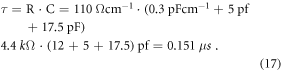
In our circuit, we consider the total resistance of the wires, from the electrode until the connection to the external device. Assuming the worst case scenario, we consider wires with a total length of 40 cm and 10 μm width with an interline distance of 10 μm with a resistance of 110 Ωcm−1 and a capacitance of 0.3 pFcm−1 [43] resulting in a total wire resistance from the electrode to the external device of 4.4 kΩ and a capacitance of 7.5 pF. Assuming three wires in our schematic, one from the brain electrode to the CMOS switch, a second wire between the CMOS switch and the amplifier and a third wire between the amplifier and the external device, the parasitic capacitance of these components is estimated as:
We estimate that 0.9 μS are required to transmit the signal from the electrode to the external device when the switch is on. To estimate the resolution of the sampled signal by our multiplexer, we use the following equation:

where Ton-off is on-off time of the CMOS switch. This time is determined experimentally because it depends on the speed of the microcontroller to turn on and off the CMOS switch for a change in the input clock.
2.3.3.1.1. Noise and signal to noise ratio (SNR)
For a digital system, the SNR is given by the following equation [57]

For the mixed architecture, the SNR can be computed replacing equation (19) with equation (18).

Comparing equations (19) and (20), we observe that increasing Q, causes an increase in the SNR for a digital system. Moreover, reducing τ (equation (21)) causes an increase in the SNR of the mixed architecture.
2.4. Power consumption of the mixed architecture for ECoG implants
It is very important to consider the power consumption of implanted electronics. It is not recommended to implant devices that require more than 40 mW cm−2 because this power density produces an increase [62] of +/−2 °C and a temperature arround 45.3 °C produces necrosis [63]. Moreover, according to Harrison, anything above 80 mW cm−2 produces necrosis [64].
Considering these figures, it is very important to maintain power consumption under 40 mW cm−2. For this reason we chose a distributed architecture where the density of power consumption is distributed on the ECoG across a larger area.
3. Methods
This section describes the experimental setups used to compare the digital and the mixed architecture. Both experimental setups used the same μC, the PIC 16F1503. For the digital architecture two μC were used, one for analog digital (A/D) and one for digital analog (D/A) conversion.
Both architectures are compared using the following criteria:
- 1.The maximum bandwidth free of aliasing with the mixed and the digital architecture will be measured. For this purpose, the SNR and the cross correlation coefficient [65] between original input signals and reconstructed signals from the mixed and the digital architecture will be used.
- 2.The quality of the recorded signals with the mixed and the digital architecture will be compared based on their SNR and the cross correlation coefficient with the original input signals.
- 3.The value of the duty cycle of the recorded signal, parameter d in equation (11), will be varied and its influence on signal quality will be investigated.
- 4.The power consumption of both architectures will be measured. It will be ensured that a power density of 40 mW cm−2 is not exceeded, as described in section 2.4.
3.1. Maximum sampling frequency and maximum bandwidth for both systems
A model of the mixed and digital architecture was created to estimate the maximum bandwidth of the recorded signals that can be obtained with these architectures (figure 12). The maximum bandwidth of the mixed architecture depends on the internal speed of the μC and the number of instructions executed internally in the μC. The maximum bandwidth of the digital architecture and the mixed architecture is defined as the bandwidth at which the SNR and the cross-correlation just start to decrease. By comparing these parameters, it is possible to compare the bandwidth of one system with the another.
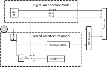
Figure 12. Digital (top) and mixed architectures (bottom) with an independent clock. G is the signal generator. The Switch S can conect the clock input of the mixed system to the clock line of the digital system (Syncronic mode) or with an external Clock (clock asynchonous). In the case of the digital.
Download figure:
Standard image High-resolution imageThe maximum bandwidth will be determined experimentally with an external oscillator as a clock input of the mixed system which will be varied to control the sampling frequency of the μC. In this schematic, it is possible to switch the clock input of the microcontroller between the clock of the digital system or the external oscillator. These have the same frequency as the clock of the digital system.
3.1.1. Setup for comparing the mixed and digital architecture
The goal is to prove experimentally equation (12) by comparing the mixed and the digital architectures fixing Q and d and comparing the effect on the data rate of the PCM  and PAM signals (
 ). For this purpose, both architectures were synchronized using the same clock turning the switch (S) of figure 12 to 1. Them the sampling rate of both systems and their effect on the quality of the recorded signals could be compared. Synchronizing the clocks causes both the mixed architecture to start transmiting the recorded samples from the electrode andthe digital architecture to start transmiting the data.
As mentioned earlier we use the same μCs in both architectures for a fair comparison resulting in a data transmission time of 40 μs and an A/D conversion time of 50 μs. Moreover, the input samples are transmitted at the same time in both allowing a fair comparison. In the mixed architecture, it results in us being able to use it to take samples from the input sigalt approximately (40 μs/(40 μs + 50 μs)) * 100 = 45% of the total timel because this architecture can read and transmit the samples simultaneously and synchronously with the clock. The mixed architecture was also tested with a separated non-synchronous clock (switch S in 2 position, figure 12).
The digital system has a conversion time and it depends on the number of instructions in the μC program to read/write from/in the registers and the internal clock configured in the μC. The advantage of the mixed architecture is that this conversion time does not exist. In the results section, we compare how many extra samples can be transmitted by the mixed architecture during the conversion time required by the digital architecture
3.2. Analysis of real biological signals with the mixed and the digital architectures
In this section, the behavior of our systems with real recorded biological signals were tested. Biological signals recorded through an ECoG in a Guinea pig, including local field potentials (LFP, less than 300 Hz) and action potentials or spikes (AP, more than 300 Hz) using stimulation [66], were recorded and stored in digital format. These signals were presented through a signal generator (G) as an input to the digital and the mixed architectures (see figure 12).
LFPs and APs from the auditory cortex of a guinea pig were recorded under Isoflurane anesthesia. For this purpose, a Neuronexus Microelectrode array of 32 channels (electrodes of 177 μm2, IrOx) was used. The electrode was placed in layer 5 of the auditory cortex. For the LFP, the data were recorded using an AlphaOmega SnR electrophysiology system (22 000 Hz sampling rate, 16 bit resolution, 1 Hz–9000 Hz filtered) and transferred to '.wav' format via Matlab (Mathworks, Inc., Natick, MA). The AP was filtered with a 2nd order Butterworth, 0-phase-lag band pass filter with cut-offs 300 Hz–3 kHz implemented in Matlab (filtfilt-function). The recorded signal was also stored in –wav format. These signals were amplified and reproduced through a sound card. The electrical output of the sound card had a peak to peak amplitude of 300 mv and an offset of 300 mV to guarantee positive values. Otherwise these signals could not be directly recorded by the μCM of the digital system.
The quality of the reconstructed signals with the mixed and digital architectures was assessed aligning the input and the output signals and then computing the pearson correlation coefficient between the input and the aligned output signal for each system. The correlation can be computed as shown in equation 21:
where  denotes the time index,
  denotes the length of the input/reconstructed signals,
  and
and  are the values of the input and the reconstructed signals at time index
 and
and  are the mean of the signals
  and
and  and
and  and
and  are the standard deviations of the signals
  and
and  The time delay at which the correlation coefficient is largest is denoted by τ. Both the correlation coefficient
  and the time delay τ are analyzed for the digital and the mixed architectures in the results section. We calculate the correlation coeficient using the function corr with Matlab. Moreover the SNR was defined as:
3.3. Effect of the d parameter
Here we will assess the effect of d in equation (12) on the data rate of the mixed architecture. For this purpose, we used the setup presented in figure 12 to change the Switch s to the position 2 (asynchronous). We will repeatedly record signals from a single electrode for different values of d. For this purpose, we programmed the stack sequence of the μC, figure 13 presents an example for d = 1/2 and d = 1/4.
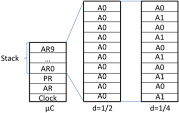
Figure 13. Stack programming for different values of d. A0 denotes the electrode number 0, A1 denotes the electrode 1. Where d is the duty cycle.
Download figure:
Standard image High-resolution imageBased on the presented setup we will prove that the sampling frequency of one channel is reduced each time that d is reduced. This reduction of d will be produced because more channels have to be recorded causing an increase of the equivalent data rate required to transmit the PAM signal, as predicted by equation (12).
3.4. Power consumption
The power consumption of both architectures is measured using current and volt meters at their inputs. Figure 14 presents the schematic of the used electronic circuit.
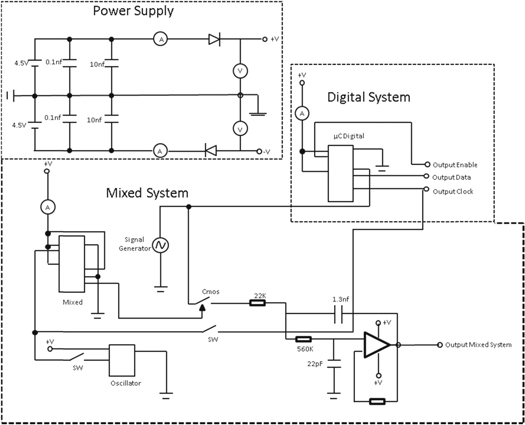
Figure 14. Schematic used to compare the power consumption by the mixed and the digital architecture.
Download figure:
Standard image High-resolution image4. Results
In this section we show experimentally the theoretical concepts presented in section 2.4
4.1. Maximum sampling frequency and maximum bandwidth for the digital and mixed
First, we estimate the maximum bandwidth for the mixed and digital architecture. For this purpose, we estimate the maximum frequency of a sinusoidal signal that can be reproduced at the output of each architecture without aliasing or significant distortion. In the next experiment, note that the mixed architecture is connected to the input clock of the digital architecture as described in section 3.1.1. Figure 12 the swirch is connected in position 1, it shows the output for both architectures. The mixed architecture was configured with a duty cycle of d = 1/2 and the digital architecture was configured to transmit Q = 10 bits/sample.
In table 1, it can be observed that the mixed architecture starts to produce aliasing for an input frequency of 5 kHz resulting in an SNR of 14.45 dB. The aliasing effect is observed because the sampling frequency starts to become similar to the frequency of the input signal. Note that in this experiment, the mixed and digital architecture are synchronized and therefore, the full potential of the mixed architecture is not completely used as the mixed architecture only takes input samples while the digital architecture transmits data between the microcontroller and the computer. Figure 15 shows this effect. The mixed architecture is able to transmit 3 samples in the same time required by the digital architecture to transmit 1 sample.
Table 1. Summary of cross-correlation coefficients (rho) and SNR coefficient for the different systems.
| Input frequency | 100 Hz | 500 Hz | 1 kHz | 2 kHz | 3 kHz | 4 kHz | 5 kHz | |
|---|---|---|---|---|---|---|---|---|
| Digital | rho | 0.94 | 0.58 | 0.76 | −0.29 | 0.26 | 0.16 | 0.07 |
| Architecture | SNR [dB] | 25.79 | 12.48 | 18.53 | 2.34 | 3.92 | 2.99 | 1.87 |
| Mixed | rho | 0.99 | 0.99 | 0.99 | 0.99 | 0.99 | 0.96 | 0.84 |
| Architecture | SNR[dB] | 49.19 | 47.74 | 52.96 | 47.83 | 33.59 | 20.86 | 14.45 |

Figure 15. Syncronized systems via Clock (switch figure 12 in position 1), Comparison of sampling frequency for one channel using the mixed architecture against the digital atchitecture. The clock of the digital architecture is given in red color while the sampling in the mixed architecture is given in blue color. The time interval between bursts of clock pulses is used to perform A/D or D/A conversion by the computer and the master microcontroller of the digital architecture.
Download figure:
Standard image High-resolution imageIn the following experiment we use an independent clock (figure 12, switch in the position 2) for the mixed architecture. The recorded signals at the output of the mixed and the digital architecture are presented in figure 16. Under this configuration, the mixed architecture is able to record samples during the time required by the digital architecture to perform the A/D conversion and vice versa. The clock signal of the mixed system has the same frequency as in the digital architecture.
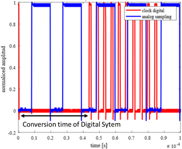
Figure 16. Asynchrponous mode (switch figure 13 in position 2): Comparison of sampling frequency of one channel for the mixed architeture against the digital architecture for a separated free running mode clock.
Download figure:
Standard image High-resolution imageFigure 16 demonstrates that with the mixed architecture configured with an independent clock, it is possible to reproduce an input signal of 10 kHz with a correlation coefficient (rho) of 0.83 and an SNR of 17.45 dB (see figure 17). In contrast the digital architecture only obtains an SNR if 10.3 dB and a rho coefficient of −0.01. Table 1 presents the SNR and rho values for different frequencies using both architectures with Syncronic mode (switch in position 1 of figure 12).

Figure 17. Output signal delivered by the mixed architecture with independent clock ( switch in position 2 of figure 12) and the digital architecture for an input signal of 10 kHz. It is possible to observe the aliasing efect of the digital System, when the input frequency is reaching the Nyquist limit.
Download figure:
Standard image High-resolution imageThe results from table 1 demonstrate that the mixed architecture is indeed able to reconstruct signals with higher frequency than the digital system.
The previous results are useful to better understand equation (11). In the experiment in which both architectures use the same clock (figure12 switch in position 1) and therefore  is the same for both architectures, the data rate of the system is 500 kbps with a maximum bandwidth of 1 kHz for the digital architecture. We have shown that for this configuration, the mixed architecture can transmit a signal with a higher frequency. For this reason, we can reinterpret through the corollary of the equation (11). Looking at equation (11), theoretically the data rate of the mixed architecture
  can be increased by a factor of
  For the parameters used in the experiment, Q = 10 and d = 1/2 resulted in
  This means that the bandwidth of the signal, which can be transmitted through an analog-digital system should be a factor of 5. If we consider that the digital system has a maximum bandwidth of 1 kHz with a rho of 0.76. We can expect that the mixed architecture can transmit with a maximal bandwidth of 5 kHz. As we can observe, the maximal bandwidth with both system working synchronically for the mixed architecture, the rho is 0.84 at 5KHz. The rho is very low for a factor of 5, up this frequency. In this case, it should be considered that the sampling is not constant and for this d is less than we can observe in figure 15.
However, note that in the case of independent clocks, the experiments show that it is possible to improve the theoretical rate presented in equation (11). We experimentally obtained a data rate of around 10 kHz (see figure 17) with a good reconstruction of the signals, reasulting in a rho = 0.83. This data rate could be further extended to 15 kHz, although the amplitude of the amplitude of the reconstructed signal is reduced by the reconstruction low pass filtering.
4.2. Biological signal test and cross correlation
In this section, the mixed and the digital architecture are used to record LFP and AP. The quality of the reconstructed signals using the mixed and the digital architecture are compared to each other based on the cross correlation coefficient (rho) between the input and the reconstructed signals as well as the delay at which this correlation is largest.
In the first experiment, the clock of both architectures is synchronized. Figure 18 presents the input LFP and the reconstructed LFP using the digital and the mixed architecture.
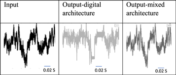
Figure 18. LFP for both architectures using the same synchronized clock.
Download figure:
Standard image High-resolution imageFigure 18 shows that the mixed architecture obtains a much better reconstruction of the LFP than the digital architecture. Note that for the digital architecture, it was necessary to introduce an offset to the input signal such that it was always positive as the A/D converter cannot convert negative signals.
Figure 19 presents the same analysis using APs as input signals.
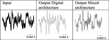
Figure 19. AP for both architectures using the same synchronized clock.
Download figure:
Standard image High-resolution imageThe results from figure 19 show again that the mixed architecture obtains a better reconstruction than the digital architecture. The main reason for this being the fact that the sampling rate of the mixed architecture is 5 times higher than the sampling rate that can be achieved with the digital architecture (equation (12)).
So far we tested the reconstruction of signals with both systems using synchronous clocks. However, as already mentioned, the mixed architecture system can transmit an increased amount of samples if independent clocks are used. For this reason, we repeated the previous experiments using a clock of 5000 kbps for the mixed architecture. Figure 20 presents the recorded and reconstructed AP for the mixed system with an asynchonous clock.

Figure 20. AP for the mixed architecture with asynchonous clock.
Download figure:
Standard image High-resolution imageComparing the results from figures 19 and 20 we can see that the reconstructed signal improved using an independent clock. Table 2 summarizes the correlation coefficient for each architecture using LFPs or APs as input signals and using synchronized or independent clocks only for the mixed architecture. The results of the table show clear advantages for the mixed architecture as expected from previous experiments and the theoretical analysis provided in equations (11) and (12). From table 2, it can be observed that the largest differences in quality of the reconstructed signals for the mixed and the digital architectures occur when APs are used as input signals, as these signals are faster the LFP.
Table 2. Cross correlation coefficient for the digital and the mixed architecture using synchronized or independent clocks using local field potentials (LFPs) or action potentials (APs) as input signals.
| Synchronized | Independent | ||||
|---|---|---|---|---|---|
| LFP | AP | AP | |||
| Digital | Mix | Digital | Mix | Mix | |
| Cross correlation | 0.86 | 0.99 | 0.76 | 0.98 | 0.99 |
| SNR | 23.13 | 55.63 | 17.63 | 45.63 | 48.56 |
4.3. Effect of the duty cycle d
From equation (11), it can be observed that two parameters that determine the data rate are the duty cycle d of the mixed architecture and the Q parameter of the digital architecture. In the mixed architecture, reducing d causes a decrease of the sampling frequency ( ). In the digital architecture, if Q is reduced, the transmission data rate will increase but the resolution of the recorded signal will become worse. The following paragraphs compare the best performance of the digital architecture with the worst performance of the mixed architecture. The mixed architecture was configured with different values of d = 1/4;1/6;1/8;1/10 (figure 21).

Figure 21. Sampling frequency of the mixed architecture for different values of d (duty cicle = tpam/Ts).
Download figure:
Standard image High-resolution imageIn figure 21, it can be observed that increasing the number of channels and therefore reducing d, causes the sampling frequency in each channel to be reduced. The maximal input clock frequency is achieved, when the sampling frequency is achieved. This reduction of the sampling frequency is expected as shown in equation (11).
There is an oscillation caused by the Sallen-Key low pass filter used. For this reason, a low pass filter was inserted at the feedback of the Sallen-Key to reduce the oscillatory effect. The result of adding this extra filter is shown in figure 22 using an AP as input signals and d = 1/20.

Figure 22. Mixed architecture output with an AP input for d = 1/20 with low pass filter at the feedback loop of the Sallen-Key filter.
Download figure:
Standard image High-resolution imageAs a consequence of adding this filter, it is now possible to transmit 10 analog channels (d = 1/20) with a rho of 0.79 and a SNR of 32.24, which is considerably higher than what can be achieved with the digital architecture, as shown in these experiments configured with 500 kbps.
4.4. Power consumption
In our experimental setup for the mixed system we used a μC and 6 CMOS switches with a voltage of 1.8 Volts that required 700 μA and therefore resulted in 1.2 mW. This μC with 6 CMOS switches is the smallest control unit of our architecture (figure 2) that we term cell. Given that the dimensions of the cell are 1 cm2, the resulting power consumption density is 1.2 mW/cm2. On the other hand, the digital system has a power consumption of 1.2 mW by the microcontroller of the digital architecture. This means that the energy consumption in the two architectures is the same, but the quality of the signals transmitted with the mixed system is higher.
5. Discussion
5.1. Summary of the architecture
ECoG are used in surgery for the diagnosis of epilepsy [31]. Several studies have shown that increasing the number of electrodes can improve the diagnosis of epilepsy [30]. To maintain the flexibility of the array, we proposed a distributed multiplexing architecture [43] with an analog transmission system. In this study, we have shown that using the same hardware it is possible to increase the number of multiplexed electrodes with an analog data transmission instead of digital a digital transmission architecture.
Both architectures were analyzed and compared in terms of the quality of the reconstructed signals they can deliver. Results showed a higher correlation between input and reconstructed signals with the mixed architecture than with the digital architecture. The cross-correlation coefficient (rho) for a single channel in a digital system was 0.76 for the digital architecture and 0.99 for the mixed using a sinusoidal signal of 1 kHz as input signal. This frequency corresponds with the typical bandwidth of an AP. For a frequency of 400 Hz, corresponding to a high gamma signal of a LFP, the correlation coefficient rho with mixed architecture was 0.994 and for the digital architecture was 0.86.
The theoretical improvement that can be achieved using a mixed architecture was shown through the corollary of equation (11) which shows that it is possible to increase the bandwidth of the recorded signal for the mixed architecture  In our implementation, we used Q = 10 bits and d = 1/2, that resulted in an improvement with a factor of 5. We also used biological signals (APs and LFPs) and compared their reconstruction quality using the mixed and the digital architecture. The differences in quality between both architectures were more prominent for APs as these signals require an increased bandwidth, in which the advantages of the mixed w.r.t to the digital architecture can be exploited.
Reducing the value of d, which is equivalent to an increase in the number of channels, decreases the quality of the reconstructed signal (rho decreases). In our experiments, we show that for d = 1/20, the quality of the reconstructed signals with the mixed architecture is higher than the digital architecture. Therefore, using the mixed architecture to reconstruct AP signals, it is possible to transmit 10 channels with a higher correlation coefficient than with the digital architecture. It would even be possible to further reduce d to achieve the same quality with the mixed and the digital architecture. With the mixed architecture presented here, it is possible to preselect the electrodes from which we want to record signals using an external device. In this way it is possible to configure the system to record the LFPs of a subset of electrodes and increase the sampling to improve the reconstruction of APs. We have shown that the mixed architecture introduces no delay due to the A/D conversion analog which gives an advantage in sampling frequency. The sampling frequency can be increased, because during the A/D conversion time it is possible to take additional samples of the input signal. It is important to say that both architectures were implemented in the same microcontroller and synchronizing the frequency of the internal clocks. In this way, it is possible to show that the mixed architecture achieves a higher sampling frequency than the digital architecture with an acceptable SNR.
We develop here an electronic architecture that can be used for ECoG to transmit the signals in an analog instead of digital format. There are other works that proposed this idea [67–70]. These multiplexers make matrix, array controlled by transistors, that reduce the amount of wires.However as the number of electrodes increases, the amount of cables also increases, but in a smaller proportion, instead of decreasing. In contrast, our proposed mixed architecture increases the number of wires without increasing the number of lines used to control the array. This was accomplished just by increasing the number of internal registers in the microcontroller to allow for more electrodes. Another possibility is to use microcontrollers with longer (larger amount of bits) registers.
One limitation could be that as the number of electrodes increase, the noise in the line could rise too. For this reason, it could be necessary to use an amount of cells and make blocks. Equation (11) compared the data rate of the digital architecture and the mixed architecture. The ratio between both data rates was experimentally proven using the same hardware. It needs to be considered that hardware elements (internal delays or the A/D conversion time) can affect this ratio. To avoid these problems and to give the same conditions, we use the same hardware in our experiment.
The thermal and mechanical considerations are described in appendix A comparing the components used in our mixed architecture against other existing technologies such as Intan chips. Table A1 compares the energy densities of the chips used in our architecture. It can be seen that the energy density of the Intan chips is higher than the limit mentioned above of 40 mW cm−2, which means that these arechitectures are not suitable for implantation. On the contrary, the chips used in our architecture are far below this limit. Table A1 compares the stiffness of the the Intan chips and the stifness of the chips used in our architecture. In this table we can see that the chips based on the mixed architecture presented here have a stiffness of 18, which is 18 times lower than the Intan chips, because these are smaller. Table A1 considers all the parameters already mentioned above, in this case the analysis could be extened considering chips with analog-digital converters with different bit resolutions. It can be observed that processors that have different package dimensions or energy consumption are not suitable for implantation because of their large size and high stifness or because they have high energy consumption requirements. Because of these considerations, we assumme that the 16F1503 chip with the CMOS TS5A3157 is the optimal hardware combination for implantation. However, results related to the transmission of the neural signals in analog instead of digital form should be replicable, irrespective of the hardware used.
Table A1. (A) Comparison of power consumption and power density of Intan chips and our chips correspodning with the mixed architecture. (B) Comparison of stiffness of Intan chips and our chips based on the mixed architecture. (C) Comparison of power consumption and power density of different chips with different bit resolutions and our chips based on the mixed architecture.
| Chip | Length(cm) | Width(cm) | Power consumption (mW) | Density power consumption (mW cm−2) | Implantable (<40 mW cm−2) | ||||
|---|---|---|---|---|---|---|---|---|---|
| (A) | |||||||||
| RHA2000 QFN | 0.8 | 0.8 | 96 | 150 | No | ||||
| RHA2000 Barr die Size | 0.48 | 0.31 | 96 | 645.16 | No | ||||
| RHD2000 QFN | 0.8 | 0.8 | 37 | 57.81 | No | ||||
| RHD2000 Barr die Size | 0.48 | 0.41 | 37 | 188.01 | No | ||||
| our arquitecture | |||||||||
| PIC16F1503 | 0.3 | 0.3 | 1.28 | 14.2 | Yes | ||||
| TS5A3157 | 0.3 | 0.17 | 0.02 | 0.34 | Yes | ||||
| (B) | |||||||||
| Chip | Length(m) | Widh(m) | High(m) | young's modulus (N m−2) | Stiffness (Nm2) | ||||
| RHA2000 QFN | 0,008 | 0,008 | 0,0008 | 1.10−10 | 0,034 | ||||
| RHD2000 QFN | 0,008 | 0,008 | 0,0008 | 1.10−10 | 0,034 | ||||
| our arquitecture | |||||||||
| PIC16F1503 [71] | 0,003 | 0,003 | 0,0005 | 1.10−10 | 0,002 | ||||
| TS5A3157 | 0,003 | 0,00175 | 0,0008 | 1.10−10 | 0,003 | ||||
| (C) | |||||||||
| Chip | Bit resolution | Length(m) | Widh(m) | High(m) | Young's modulus (N m−2) | Stiffness (Nm2) | Voltage (V) | Current (A) | Density of power consumption |
| PIC16F1503 | 10 | 0,003 | 0,003 | 0,0005 | 1.1010 | 0,002 | 2 | 0,0006 | 14,22 |
| EFM8BB31F64G | 12 | 0,003 | 0,003 | 0,0008 | 1.1010 | 0,0048 | 2 | 0,005 | 111,11 |
| EFM8LB11F32E-B | 14 | 0,003 | 0,003 | 0,0008 | 1.1010 | 0,0048 | 2 | 0,015 | 333,33 |
| MK20DX128VFM5 | 16 | 0,005 | 0,005 | 0,0009 | 1.1010 | 0,016 | 2 | 0,015 | 120 |
| CY8C5888LTI-LP097 | 20 | 0,008 | 0,008 | 0,001 | 1.1010 | 0,05 | 2 | 0,005 | 15,62 |
| dsPIC33EP512MU810-I/PF | 24 | 0,014 | 0,014 | 0,001 | 1.1010 | 0,16 | 3 | 0,02 | 30,61 |
| STM32F302xB | 32 | 0,0072 | 0,0072 | 0,0015 | 1.1010 | 0,09 | 2 | 0,1 | 385,80 |
The intention of this paper was to demostrate the advantages of the mixed architecture w.r.t. a pure digital architecture. For this purpose, it was enough to generate analog signals through a sound card. Still we admit that in the future the proposed architecture should be implemented and combined with an amplifier to get a more realistic setup.
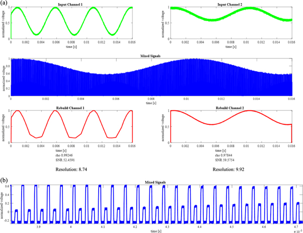
In the mixed architecture the distance from the ECoG electrodes to the amplifier going through the CMOS switch is estimated to be around 10 cm. We estimate that the cable between the amplifier to an external PC would be around 30 cm. This relatively long cable using analog transmission will indeed act as an antenna and may capture undesired noise and interferences including the 50 Hz line noise (which can be atenuated with a notch filter) and radio frequency signals going from AM to RF signals spanning the range of kHz to GHz. These radiofrequency signals however are high enough that they do not interfere with the low frequency of local field potentials. For sure, in an operation theater several other sources will impact the bandwidth corresponding with local field potentials and this is an issue that has not been considered in the current study. Still, the proposed mixed architecture offers several advantages w.r.t. for an implanted digital architecture; this includes (1) the use of a single amplifier for all ECoG electrodes versus a one amplifier for each electrode in the digital architecture; (2) A higher bit resolution as current implantable digital architectures are limited to 10 bits; (3) The possibility to record higher frequency signals through multiplexing. In figure B1 of appendix B, it is shown how it is possible to achieve this principle of signal multiplexing for two channels. It can be shown that it is possible to multiplex two channels and reconstruct the original signals from the multiplexed signal with a bit resolution greater than 8.5, an SNR greater than 50 dB and a cross correlation of 0.99 for sinus signals.
Figure B1. (A) Two channels signals multiplexed and separated, bit resolution of 9.9 Bits for channel 2 and 8.74 for channel 1. (B). Zoom, Mixed signal from channel 1 and channel 2.
Download figure:
Standard image High-resolution image
6. Conclusion
ECoGs are used for the diagnosis of neurological diseases such us Epilepsy. Increasing the number of electrodes contacts can help improving the diagnossis of epilepsy. However, increasing the number of electrodes causes an undesired rise in the number of wires which in turn causes an increase in the stiffness of the array. It is desired to produce flexible implantable devices that adapt with the surface of the brain. To achieve this aim, we propose an electronic architecture to multiplex the signals coming from the electrodes, while at the same timereducing the number of wires needed to record the signals and the stiffness of the array. We show that by using a distributed electronic architecture integrated into an ECoG it is possible to transmit signals captured by ECoG electrodes in the analog domain. Using this novel architecture, it is possible to increase the number of electrode signals by a factor of 10 with respect to an equivalent digital architecture without increasing power consumption or the internal clock frequency.
Acknowledgment
We appreciate the support of this work from DAAD, project 57129429 as well by the German cluster of excellence Hearing 4 All. We are grateful to Tom Gajecki for his help in MATLAB modelling and to Mathias Voigt to share the signals recording of LFP and AP according to approval number 17/2436 by LAVES.
Appendix A
This appendix presents several tables comparing power density consumption with different existing commerical products and our mixed architecture.
Appendix B
In this appendix we show that it is possible to extend the analysis done for 1 electrode channel to 2 electrodes channels for the mixed architecture. Moreover, we evaluated numerically the reconstructed signals of these two input signals into Channel 1 and Channel 2.