
Abstract
Single quantum emitters (SQEs) are the basic building blocks for quantum optics and quantum information technology. Strain-induced defects in monolayer transition metal dichalcogenides (TMDs) have been shown to be a promising platform for the generation of SQEs. In particular, achieving optically active and electrically controlled quantum emitters make these materials attractive for applications ranging from quantum communication and optoelectronics to high resolution metrology. Here, we report the spectral photoresponse of monolayer WSe2 upon strain, where we observe a connection between single-photon emission and photocurrent (PC) generation in a p-n device. A strong antibunching in second-order correlation from this localized emitter unambiguously demonstrates the single-photon nature of the emission, whereas the PC is highly dominated by the absorption at such a localized state, showing an exponential dependence with the applied electric field. Furthermore, we can resolve narrow PC peaks with 1.0 meV spectral width.
Export citation and abstract BibTeX RIS

Original content from this work may be used under the terms of the Creative Commons Attribution 4.0 license. Any further distribution of this work must maintain attribution to the author(s) and the title of the work, journal citation and DOI.
1. Introduction
Single quantum emitters (SQE) represent an unique system in which optical radiation is composed by solely one photon at a time, constituting the base for many applications such as quantum information processing [1–3], quantum networks [4] and quantum computing [5]. In atomically thin transition metal dichalcogenides (TMDs) [6–8], local non-uniform strain variations (e.g. near the edge of nanostructures [9, 10]) in combination with a large defect density enables efficient funneling of bright excitons into localized states [11], which leads to the formation of SQEs [10, 12–15]. This feature has been particularly exploited in tungsten diselenide (WSe2) [9–11, 16–20] in several applications, including quantum light-emitting diodes [21, 22], strain-induced arrays of QEs [10, 16] and voltage-controlled quantum light [23, 24]. Nevertheless, these studies are commonly focused on the light emitted from such defects, although little is known about their optoelectronic counterpart, i.e. the conversion of photons into an electrical current at such localized states.
The photocurrent (PC) of self-assembled quantum dots (QDs) in III–V p-n junctions or Schottky diodes has been widely studied in the past, where the absorption spectra resembles discrete resonant peaks related to the QDs energy [25–28]. Here we report the resonant PC spectroscopy of single-quantum emitters induced by strain in a monolayer WSe2 p-n junction. We find that, at cryogenic temperatures, the spectral photoresponse matches the corresponding photoluminescence (PL) with an enhanced photoresponsivity peak at the SQE energy. We also observe that the responsivity measured at the SQE has an exponential dependence on the applied electric field, thus suggesting a tunneling-mediated dissociation mechanism. Moreover, the photoresponse shows excellent spectral stability at low temperatures and a linewidth of ∼1.0 meV (FWHM), which is more than one order of magnitude smaller than that measured in the same sample from delocalized excitons (linewidth ∼78 meV FWHM), and similar to the one observed in previous reports [29, 30]. Our results expand studies on the light–matter interaction to localized states in two-dimensional materials and establishes a relation between light emission and absorption in these systems.
2. Results and discussion
The device structure used to study the PC from localized states is schematically depicted in figure 1(a). A monolayer WSe2 flake is transferred over the edge of a pillar structure, fabricated as follows: first, a Ti/Au pillar (5 nm/100 nm) is patterned on a SiO2 substrate by standard e-beam lithography. An Al2O3 layer with 20 nm thickness is grown afterwards by atomic layer deposition on both the SiO2 substrate and the Au pillar, providing an insulating layer over the Au pillar, which will be then used as back-gate electrode. Then, a monolayer WSe2 flake is transferred on such a structure while taking care of placing part of the flake on the Al2O3/Au (Au pillar hereafter) region and the other part on the Al2O3/SiO2 (Al2O3 substrate hereafter) region. A monolayer sheet transferred on such a structure exhibits high strain at the step-edge which, combined with the present of large defect densities, forms localized states in WSe2 [6, 9–12, 16–20]. Excited free excitons then diffuse towards the local regions with strain-tuned band-gaps and become the source of SQEs. Note that the height (h) of the sample structure is crucial to strain the atomic layer at the step-edge, i.e. the higher the structure, the stronger is the strain. The optical properties of the WSe2 layer change in these regions, where the excitonic energy levels are locally shifted down in energy [10, 31, 32]. Other methods employed to study PC in strained 2D materials involve the use of flexible substrates [33–35]. For the transfer process we use an all-dry transfer technique [36]: first, WSe2 bulk crystals (grown by vapor phase transport, see Ref [37]. for details) are mechanically exfoliated using an adhesive tape, and the obtained thinner flakes are again exfoliated by means of a polydimethylsiloxane stamp (Gelfilm form Gelpak). The atomically thin layers are then identified by a combination of optical contrast and Raman spectroscopy [37]. In order to transfer the WSe2 monolayer sheet on the nanostructure we used a deterministic transfer method [36]. Finally, Ti/Au (5 nm/200 nm) drain-source electrodes are fabricated by e-beam lithography and metal evaporation, one contacting the flake on the Al2O3 substrate and the other one on the Au pillar to probe the current flow through the strained region. The distance between the contact electrodes is 1.5  m. Figure 1(b) shows a false-color scanning electron microscopy image of the sample.
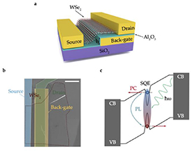
Figure 1. (a) Schematic sketch of the device structure with monolayer WSe2 over a step (height h = 105 nm). The WSe2 flake is contacted by Ti/Au (5/200 nm) electrodes and separated from the back-gate electrode by a 20 nm thick gate dielectric (Al2O3). (b) False-color scanning electron image of the device (Scale bar, 5 μm). (c) Schematic band diagram of a SQE photodiode for negative drain-source voltage (VDS). Following resonant optical excitation, single electron-hole pairs are generated and dissociated at the junction, which results in a PC.
Download figure:
Standard image High-resolution imageWe focus our studies on the PC generated at SQEs formed due to strain at the step-edge mentioned above. To illustrate the basic concept of the PC generation in a localized state, we use the simplified band diagram displayed in figure 1(c) in reversed bias, i.e. for a negative drain-source voltage (VDS). The spectral photoresponse of localized states is studied by probing the drain-source current through the strained material while tuning the excitation wavelength. Hence, when the impinging photon energy matches that of the SQE, the photon is directly converted into an electron-hole pair, thus forming a localized exciton. The external applied electric field, in reversed bias, causes the dissociation of such localized excitons, leading to a PC generated by the resulting free carriers. This is in contrast to non-resonant photoluminescence (PL) spectroscopy, where the optical excitation energy is constant and higher than that of the optical band gap.
We first present the electrical characterization of our device (sample A). The transfer curve, measured by sweeping the back-gate voltage (VBG) at a constant VDS, shows a clear ambipolar nature (figure 2(a)), implying that the doping across the WSe2 channel can be electrostatically tuned both n- and p-type [29, 38–40]. Furthermore, the current–voltage characteristics (IV hereafter) show diode-like rectifying behavior (figure 2(b)), producing a photovoltaic effect upon illumination with white light (power density Pd ≈ 0.2 W cm−2), characterized by the shift downwards of the IV curve, thus generating a short-circuit current and an open-circuit voltage [38, 39]. Next, we probe the absorption spectrum in the photoactive region by measuring the PC as a function of the photon energy at room temperature. For PC measurements a low-noise current-preamplifier and a lock-in amplifier (Stanford Research System SR570 and SR830) in combination with a Keithley source-meter unit (Keithley 2612 A) are used. Optical and electrical investigations are carried out in a liquid-helium flow cryostat (Oxford Instruments) under high vacuum (10–7 mbar), integrated in a scanning micro-PL/PC setup. In the PC experiments, the sample is optically excited by using a supercontinuum laser (NKT Photonics SuperK Extreme; tuning range from 400 to 900 nm with a linewidth of ∼15 meV) and a cw tunable laser source (Ti:Sapphire Spectra Physics 3900 S; tuning range from 732 to 800 nm with a linewidth of ∼200  eV). For PL measurements, the sample is optically excited non-resonantly using a continuous-wave 532 nm laser and the PL signal is collected using a 50
 long working distance objective lens (NA = 0.5). The diameter of the laser beam on the sample is 1 μm. We use a dichroic mirror at
  550 nm to separate the photon emission from the excitation. The PL emission is spectrally filtered with a monochromator (Horiba iHR320) and detected with a liquid nitrogen cooled charge-coupled device (CCD) (Horiba Symphony II). We refer the reader to figure S1(https://stacks.iop.org/2DM/7/045021/mmedia), supporting information, for an schematic drawing of the measurement setup.
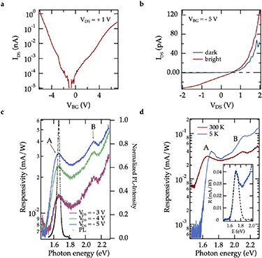
Figure 2. (a) Transfer characteristic of the device taken at VDS = + 1 V and T = 300 K. (b) IV characteristics of the device in the dark (blue) and under optical illumination (red) taken at VBG = −5 V and T = 300 K. The open-circuit voltage VOC = 0.56 V and the short-circuit current ISC = −8.61 pA. (c) Responsivity spectra for various VDS taken at T = 300 K. The PC increases with increasing negative VDS bias. The responsivity spectra around the A exciton closely matches the PL spectrum (dotted line). (d) Responsivity spectrum for VDS =−4 V at T = 300 K (red) and 5 K (blue). The responsivity spectrum at T = 5 K exhibits narrower exciton peaks due to reduced thermal broadening. Inset: Responsivity spectrum (blue dots), the data are fitted by a Gaussian function (black dashed line). The extracted linewidth of the responsivity from the A exciton is ∼78 meV (FWHM).
Download figure:
Standard image High-resolution imageIn figure 2(c) we present the photoresponsivity (R) spectrum, defined as the ratio of the photogenerated current (IPC) and the incident light power (Popt): R = IPC/Popt, for different VDS. Apart from the A exciton, centered at 1.65 eV, we observe a pronounced peak at a photon energy of 2.10 eV, which is attributed to the B exciton. The features A and B stem from band-edge excitons in WSe2 residing at K points of the Brillouin zone due to the spin-orbit splitting of the valence band [29, 30, 41]. At low temperature (T = 5 K), a steeper photon absorption edge is obtained as well as narrower exciton peaks due to reduced thermal broadening (figure 2(d)). We also observe the well-known blue-shift of the exciton energy when reducing the temperature [13]. The inset of figure 2(d) illustrates a Gaussian fit of the linewidth of the photoresponse from the A exciton, centered at an energy of 1.709 eV.
We now move to the study of the optoelectronic features appearing near the step-edge of our structure. Figure 3(a) displays the spatially resolved PC image, measured with VDS = −4 V/VBG = −4 V, and an excitation photon energy of 1.68 eV and Pd = 30 W cm−2. Interestingly, the optical and optoelectronic features of the atomic layer change at locations where the monolayer is strained, i.e. at the step-edge [12, 31, 32]. In both PL and PC, sharp single peaks are observed in the spectra, attributed to single-photon emission (PL) and its corresponding absorption (PC). Hence, by tuning the excitation energy the spectral absorption of a single-photon emitter can be monitored via the IPC (figure 3(b)). We observe two peaks, one at an energy of 1.6798 eV and the second one at an energy of 1.6878 eV, referred to as localized excitons [11, 15]. For the normalized PL spectrum (excitation λ = 532 nm, Pd = 64 W cm−2) a Lorentzian fit exhibiting a linewidth of ∼2.3 meV (full-width at half-maximum), and for the pronounced PC peak (centered at 1.6798 eV), a Lorentzian fit yields a linewidth of ∼3.5 meV (full-width at half-maximum) and a splitting of 8 meV. A similar behavior is observed in another device (sample B), shown in figure 3(c). Photocurrent and PL emission occur here at a slightly different energy (1.692 eV) due to the randomness of the strain field in our samples. For comparison, we present in figure S2, supporting information, a PC spectrum measured in an unstrained region of the device, which is substantially broader. This is another indication that the sharp peaks in figures 3(b) and (c) arise from SQEs. The deviation from the reported linewidth down to tens of microelectronvolts may be due to the used underlying substrate [11]. The PL emission (sample A) from the excitons show a saturation when increasing the optical excitation power, which results in a nonlinear dependence of the PL intensity. The PL saturation curve, presented in figure 3(d), can be described by  , where IPL is the integrated PL intensity, Isat the saturation integrated intensity, Pd is the power density of the excitation and Pn =
  W cm−2 is the power density at which IPL = Isat/2 [11, 16]. Moreover, we investigate the polarization of the SQE. In monolayer TMDs the excitonic transitions exhibit an in-plane dipole, and figure 3(e) indicates the orientation of the emission dipole of a single exciton line, centered at an energy of 1.6798 eV [42]. The polarization control of the emission is performed by rotating a linear polarizer at the output path of the measurement setup, where the change in the photon count rate from the SQE is monitored using a liquid nitrogen cooled CCD detector in conjuction with a monochromator. A dichroic filter that absorbs light below 550 nm is used to eliminate incident laser light from the detector. The polarization-dependence of the PL intensity can be reproduced by using a Malus-law fit:
  , where ϕ is the polarization emission angle, represented by the solid line in figure 3(e).
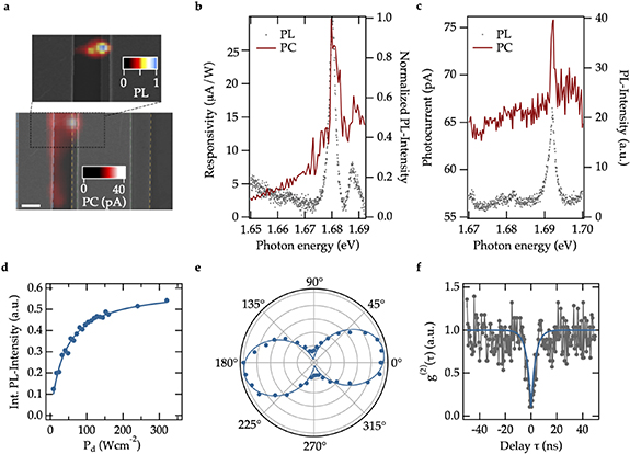
Figure 3. (a) Resonant PC map at low temperate (T = 5 K), with an excitation energy of 1.6798 eV (738 nm) and VDS = −4 V/VBG = −4 V. Inset: Normalized PL map, spectrally filtered at a photon energy of 1.68 eV (Scale bar 5 µm). (b) Responsivity spectrum (red line) measured at the bright spot in a, which closely matches the PL spectrum (grey dots), with VDS = −4 V/VBG = −4 V. Normalized PL spectrum (excitation λ = 532 nm, Pd = 64 W cm−2) with a Lorentzian fit exhibiting a linewidth of ∼2.3 meV (full-width at half-maximum). For the pronounced PC peak (centered at 1.6798 eV), a Lorentzian fit yields a linewidth of ∼3.5 meV (full-width at half-maximum) (c) Photocurrent spectrum (red line) and PL spectrum (grey dots) from sample B, with VDS = −1 V/VBG = −4 V. (d) Integrated PL intensity of the single-photon emitter (centered at 1.6798 eV) as a function of the excitation density. Circles represent the experimental data and the line depicts a power law fit. (e) Polarization dependence of the PL intensity (circles) and a Malus-law fit  of the experimental data (line). (f) Second-order correlation function of the PL peak (1.6798 eV) under a 25 W cm−2 cw laser excitation at 532 nm. The blue line is a fit to the data, from which we extract g2(0) = 0.09 ± 0.02 and a decay time t = 3.5 ± 0.1 ns.
Download figure:
Standard image High-resolution imageTo explore the nature of the photon emission, we used a Hanbury Brown and Twiss (HBT) interferometer for second-order correlation measurements. The PL emission from the SQE is filtered by a monochromator and split into two arms for the HBT correlation setup, using a non-polarizing 50:50 beam splitter. The photons are detected by two single-photon counters (Excelitas SPCM-AQRH-14-TR) with a time resolution of 250 ps. The correlation histogram is analyzed by using a two-channel time-correlated single-photon-counting module (PicoHarp 300). Figure 3(f) shows the second-order correlation function from the pronounced PL peak (1.6798 eV) under a 25 W cm−2 cw laser excitation at 532 nm, exhibiting strong photon antibunching. The fit of the second-order correlation function obtained in the experiment is modelled with:  , where t is a characteristic time for photon antibunching and A is the antibunching depth. A fit to the data at zero time delay yields to g2(0) = 0.09 ± 0.02, which is well below the threshold of 0.5, and thus, unambiguously demonstrates that it is a QE [11, 18–20, 23]. The characteristic time in the second-order correlation function, which yields the upper bound for the lifetime of the emitting state, is estimated to be 3.5 ± 0.1 ns [10, 11, 18, 19, 23].
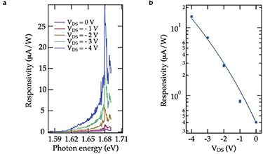
To further analyze the characteristics of the PC from a SQE, we used a laser with higher spectral resolution to measure the PC spectra around the peak of interest. The PC measurements are performed by tuning the VDS, thus allowing us to control the in-plane electric field. Figure 4(a) shows the responsivity spectra for various VDS in the photoactive configuration, with VBG = −4 V and negative VDS. We observe that the PC measured at the SQE increases with more negative voltage. Figure 4(b) shows the R peak amplitude versus VDS of the SQE, centered at an energy of 1.6798 eV, which shows an exponential behavior. Previous studies on the dissociation mechanisms governing the PC in QDs embedded in III–V p-n junctions state that at low temperatures, the dissociation of the localized excitons under reversed bias is dominated by a tunneling process [28, 43, 44]. The photoresponsivity in these systems can thus be modeled by using a simplified Fowler-Nordheim tunneling equation across the potential barrier as [45]: ![$R = {R_0}{\text{ exp}}\left[ {\frac{\alpha }{{1 + \beta /\left| {{V_{{\text{DS}}}}} \right|}}} \right]$](https://content.cld.iop.org/journals/2053-1583/7/4/045021/revision2/tdmaba4ecieqn11.gif) with fitting parameters
with fitting parameters  and
and  . The
. The  -parameter includes the built-in potential across the junction; the
  -parameter is proportional to the exciton binding energy. The solid line in figure 4(b) represents the fit of our data to this model, yielding the fitting parameters R0 = 0.4 µA/W,
  = 14.5 and
  = 12.4 V, therefore suggesting that the PC in our SQE could be explained as well by this model.
Figure 4. (a) Responsivity spectrum as a function of the applied VDS voltage at T = 5 K, ranging from VDS = 0 to−4 V with VBG = −4 V. (b) Semi-logarithmic plot of the peak amplitude, with VBG = −4 V ranging from VDS = 0 to −4 V, extracted from the responsivity spectra by using Lorentzian functions. The circles represent the experimental data, while the lines depict the fit as discussed in the main text.
Download figure:
Standard image High-resolution image
This tunneling process can be understood by using the band diagram shown in figure 1(c). At resonant illumination, i.e. when the impinging photons energy matches that of the localized state, the photon is directly converted into a localized exciton. Under an applied external electric field, the photogenerated electron-hole pair can either recombine or escape the SQE state, tunneling through the potential barrier into the conduction (electrons) or valance (holes) band of the p-n junction. Once the charge carriers escape from the barrier, they will be accelerated by the electric field, generating a PC. The charge carriers´ escape from the localized state is mainly mediated by two processes: (i) direct tunneling induced by the electric field and (ii) thermionic emission. At low temperatures, however, the thermionic emission rate is very slow and, therefore, the rapid increase of the field-enhanced photoresponse of the SQE for different VDS is likely dominated by carrier tunneling through the barrier [28, 43, 46]. In addition, for high  we expect that the photoresponse should be limited by drift-diffusive transport, and may result in a flattened photoresponse curve [43].
Furthermore, an upper limit of the electrons per second rate from the SQE can be evaluated from the experimental data in first approximation as:  109 s−1. This corresponds to a tunneling time of
  1 ns, which is of the order of typical excitation lifetimes of SQEs in WSe2 found by time-resolved PL experiments [18–20, 23]. A substantial fraction of the photoexcited excitons thus contributes to the current. Finally, we estimate an upper bound of the external quantum efficiency (EQE), which is defined as the ratio of the number of the charge carriers in the PC and the total number of impinging excitation photons and related to the responsivity R [47]:
  . Note that the obtained EQE is limited by the absorption cross section of the SQE since the illumination area is much larger than that of the SQE and, therefore, a large percentage of impinging photons do not contribute to the PC at the localized state. Besides, only one exciton can reside in the quantum emitter, reducing the EQE further [28, 43, 46, 48].
3. Conclusion
In conclusion, we have studied the spectral PC of monolayer WSe2 in a p-n junction configuration both at room and cryogenic temperature. At room temperature, the PC spectrum resembles the A and B excitons, while narrower peaks are observed at cryogenic temperatures. Furthermore, we observe single-photon emission at locations in which high strain is induced in the monolayer, characterized by a narrow line emission and strong photon antibunching in second-order correlation measurements. We find that the PC spectra match very well the PL, with an enhanced response at the same photon energy as that of the single-photon emitter. Finally, the dependence of the PC intensity with the drain-source voltage suggests that the PC at single-photon emitter locations, at low electric fields, is governed by a Fowler-Nordheim tunneling process. Our results shed light onto the optoelectronic mechanisms for quantum emitters in two-dimensional materials and provide a basis for further studies towards a deeper understanding of the underlying physics.
Acknowledgments
We acknowledge financial support by the Austrian Science Fund FWF (START Y 539-N16) the European Union (grant agreement No. 785219 Graphene Flagship; grant agreement No. 791536 Marie Sklodowska-Curie Individual Fellowship OPTOvanderWAALS), and TU Vienna (doctoral college program 'TU-D').