
Abstract
Two circular Al0.6Ga0.4As p+-i-n+ 2 µm i layer spectroscopic x-ray avalanche photodiodes (one 200 µm diameter and one 400 µm diameter) were made from a structure produced by metalorganic vapour phase epitaxy. The capacitances and currents of the detectors as functions of applied bias were measured, and 55Fe x-ray (Mn Kα = 5.9 keV; Mn Kβ = 6.49 keV) spectra were accumulated at 20 °C (293 K). Improved energy resolutions (measured as the full width at half maximum of the 5.9 keV peak) with increased applied reverse bias were observed with both detectors. In part, the improvement was attributed to avalanche multiplication. Energy resolutions of 630 eV ± 40 eV and 730 eV ± 50 eV were achieved with the 200 µm detector at an applied reverse bias of 38 V and the 400 µm detector at an applied reverse bias of 40 V, respectively. It is the first time Al0.6Ga0.4As has been demonstrated as capable of photon counting x-ray spectrometry. Measurements to determine the average electron-hole pair creation energy in Al0.6Ga0.4As were made; the results suggested a value of 4.97 eV ± 0.12 eV at 25 °C ± 1 °C (298 K ± 1 K). This value was then used to refine the apparent relationship between bandgap energy and electron-hole pair creation energy as defined by the Bertuccio–Maiocchi–Barnett relationship. AlxGa1-xAs x-ray photodiodes of this type are anticipated to be of benefit for future space missions, including those to explore the surfaces of the inner planets (e.g. Mercury and Venus) and the moons of Jupiter and Saturn.
Export citation and abstract BibTeX RIS

Original content from this work may be used under the terms of the Creative Commons Attribution 4.0 license. Any further distribution of this work must maintain attribution to the author(s) and the title of the work, journal citation and DOI.
1. Introduction
Semiconductor materials with wide bandgaps including SiC [1–3], GaAs [4–8], diamond [9, 10], Al0.52In0.48P [11–13], In0.5Ga0.5P [14, 15], and AlxGa1-xAs [16–19] have received extensive study as materials of interest for the manufacture of radiation detectors capable of operating at high (⩾20 °C) temperatures. Such research has been motivated by the limitations of conventional, relatively narrow bandgap (e.g. Si, e.g. = 1.1 eV [1]) x-ray spectrometers in use today [20, 21], which require cooling and radiation shielding to operate in many environments [22]. In the case of space science, the required radiation shielding and cooling systems of Si based x-ray spectrometers can lead to increased financial costs and technical restrictions which sometimes limit mission objectives and render certain environments inaccessible or expensive to reach. Furthermore, even when cooling and radiation shielding are used, the spectral resolution of Si detectors can degrade over time in intense radiation environments, reducing mission lifetime [23]. Wide bandgap materials, such as AlxGa1-xAs, offer an alternative. Such materials can function in relatively high radiation and high temperature environments, while providing sub-keV spectral resolutions at soft (<10 keV) x-ray energies [22].
The potential benefits of AlxGa1-xAs for spectroscopic photon counting x-ray photodiodes has driven study of Al0.8Ga0.2As [17, 24, 25] and Al0.2Ga0.8As [19, 23, 26]. However, since adjusting the Al fraction leads to changes in material and device characteristics (e.g. reducing the Al fraction leads to: a narrower bandgap; an increased linear x-ray absorption coefficient; and a better lattice match with GaAs), it may be beneficial to tailor the Al fraction of AlxGa1-xAs depending on the operating environment. For example, Al0.6Ga0.4As, with a bandgap (e.g. = 2.03 eV [27]) slightly smaller than that of Al0.8Ga0.2As (2.09 eV [27]), could optimise the material for use in more modestly elevated temperatures (e.g. space science missions to the poles of Mercury, where surface temperatures reach 70 °C (343 K) [28]).
In this work, the characterisation of two custom-made circular Al0.6Ga0.4As p+-i-n+ spectroscopic x-ray avalanche photodiodes (APDs) (one 200 µm diameter and one 400 µm diameter) at 20 °C (293 K) is presented. Each device was electrically characterised and from these results, their fundamental parameters were calculated. Using an 55Fe radioisotope x-ray source for illumination, and a custom-made charge-sensitive preamplifier connected to each photodiode in turn, x-ray spectra were accumulated for each device. The average electron-hole pair creation energy (i.e. the average energy required for the generation of an electron-hole pair at x-ray energies) was also experimentally measured for the first time.
2. Detector structure
The Al0.6Ga0.4As p+-i-n+ structure was grown on (100) n type GaAs:Si substrates by metalorganic vapour phase epitaxy. Trimethylaluminium, trimethylgallium, and arsine were used as precursors for Al, Ga, and As, respectively. Dimethylzinc:trimethylamine and disilane were used for p and n doping, respectively. Table 1 outlines the layer details of the structure. Circular mesa structures of two diameters (200 µm and 400 µm) were fabricated using 1:1:1 H3PO4:H2O2:H2O solution followed by 10 s in 1:8:80 H2SO4:H2O2:H2O solution, in Sheffield, UK, at the Engineering and Physical Sciences National Centre for III–V Technologies. Ohmic contacts consisting of 200 nm Au and 20 nm InGe were evaporated onto the base of the n+ substrate. Ohmic top contacts of 200 nm Au and 20 nm Ti were evaporated onto the top p+ side of the mesa devices. The devices were unpassivated. The p+ metal contact covered 45% and 33% of the 200 µm diameter photodiode's surface and 400 µm diameter photodiode's surface, respectivley. The devices were mounted in a TO-5 package and gold-ball wirebonded.
Table 1. Al0.6Ga0.4As p+-i-n+ structure details.
| Material | Dopant | Dopant type | Thickness (nm) | Doping density (cm−3) |
|---|---|---|---|---|
| GaAs | Zn | p | 10 | 1 × 10¹⁹ |
| Al0.6Ga0.4As | Zn | p | 500 | 2 × 10¹⁸ |
| Al0.6Ga0.4As | 2000 | Undoped | ||
| Al0.6Ga0.4As | Si | n | 100 | 2 × 10¹⁸ |
| GaAs | Si | n | 200 | 2 × 10¹⁸ |
| GaAs n+ substrate |
3. Detector electrical characterisation
3.1. Measurements of detector capacitance as a function of applied bias
For both Al0.6Ga0.4As p+-i-n+ photodiodes, device capacitance was measured under dark conditions and at a temperature of 20 °C (293 K), as functions of forward and reverse applied bias. A Keithley 6487 Voltage Source/Picoammeter and an HP 4275A LCR Meter (50 mV rms signal magnitude; 1 MHz frequency) were used to bias and measure the capacitance of the detectors respectively. The Al0.6Ga0.4As photodiodes were installed inside a custom test enclosure and placed inside a TAS Micro MT environmental chamber for temperature control. The environmental chamber was set to 20 °C (293 K) and left for 1 h before measuring to ensure thermal equilibrium; the temperature of the devices was also monitored by a thermocouple which was appropriately positioned. The test enclosure was first purged with dry N2, then sealed. The environmental chamber was continually purged with dry N2 such that a dry environment (<5% relative humidity) could be maintained, thus eliminating any humidity related effects [7]. The capacitance as functions of applied forward (figure 1(a)) and reverse (figure 1(b)) bias for the 200 µm diameter and 400 µm diameter devices is shown in figure 1.

Figure 1. Capacitance as a function of applied forward bias (a) and applied reverse bias (b) for the 400 µm (triangles) and 200 µm (circles) devices, at 20 °C (293 K). The empty package capacitance has not been subtracted.
Download figure:
Standard image High-resolution imageThe maximum forward (1 V) and reverse (40 V) biases were selected to maintain device current at relatively low levels (<1 nA) to ensure there was no damage to the devices during the characterisation procedure. For both devices, the measured capacitance increased as a function of applied forward bias; increasing from 13.13 pF ± 0.02 pF at 0 V to 19.79 pF ± 0.03 pF at 1 V for the 200 µm device, and 46.56 pF ± 0.08 pF at 0 V to 71.32 pF ± 0.11 pF at 1 V for the 400 µm device. Conversely, the devices' capacitances decreased as functions of applied reverse bias; decreasing from 13.13 pF ± 0.02 pF at 0 V to 3.96 pF ± 0.01 pF at 40 V for the 200 µm device, and 46.55 pF ± 0.08 pF at 0 V to 12.51 pF ± 0.06 pF at 40 V for the 400 µm device. The stated uncertainties included those associated with a single measurement as well as those associated with disconnecting and reconnecting the measured devices to the test enclosure.
The measured capacitance, CM, included both the diode capacitance, CD, and the package capacitance, CP, since the devices were measured after packaging. CP was removed by assuming a constant capacitance density as a function of device area. At each applied bias, the capacitance density of the 200 µm diameter device and the 400 µm diameter device was compared, and the empty package capacitance calculated. A mean average empty package capacitance (1.29 pF ± 0.19 pF) was calculated for CP and subsequently subtracted from CM of each diode. The diode capacitance densities of each device are shown in figure 2.
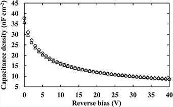
Figure 2. Capacitance density for the 200 µm device (circles) and the 400 µm device (triangles) as a function of applied reverse bias, at 20 °C (293 K).
Download figure:
Standard image High-resolution imageSince the depletion layer capacitance, CDL, under reverse bias primarily defined the diode capacitance, the depletion width, W, can be calculated using
where  is the relative permittivity of the material (11.196 for Al0.6Ga0.4As [29]), A is the device area, and 0 is the permittivity of free space [30]. The depletion width of the 200 µm device increased from 0.26 µm ± 0.02 µm at 0 V to 1.16 µm ± 0.08 µm at 40 V. Similarly, the depletion width of the 400 µm device increased from 0.28 µm ± 0.02 µm at 0 V to 1.11 µm ± 0.02 µm at 40 V. The stated depletion width uncertainty includes the uncertainty associated with the depletion layer capacitance and the uncertainty associated with the Debye length of the Al0.6Ga0.4As p+-i-n+ photodiodes (0.02 µm) [31]. The results indicated that a further increase in depletion width would be expected if the applied reverse bias was increased beyond 40 V, indicating that both detectors were not fully depleted at 40 V reverse bias. This was consistent with the device structure, which has a 2 µm i layer (see table 1). The depletion width has been plotted in figure 3(a), as a function of reverse bias; the implied quantum detection efficiency, assuming that the photodiode active region was confined to the depleted region of the i layer, has been plotted in figure 3(b).

Figure 3. (a) Calculated depletion width for the 200 µm device (black circles) and the 400 µm device (red triangles) at 20 °C (293 K), taking into account the empty package capacitance (1.29 pF); (b) calculated quantum detection efficiency for the 200 µm Al0.6Ga0.4As p+-i-n+ photodiode structure as a function of energy, assuming that the photodiode active region was confined to the depleted region of the i layer, when operated at: 40 V (dotted line), 20 V (short dashed line), 10 V (long dashed line), and 0 V (solid line) reverse bias. The discontinuities are the Al K, Ga L, and As L x-ray absorption edges. Comparable results were obtained for the 400 µm Al0.6Ga0.4As p+-i-n+ photodiode structure.
Download figure:
Standard image High-resolution imageAt the maximum reverse bias (40 V), the Al0.6Ga0.4As x-ray p+-i-n+ photodiodes quantum detection efficiency was calculated to be 0.07 at 5.9 keV and 0.05 at 6.49 keV for both the 200 µm and 400 µm device. However, since it has been shown that electrons generated in the p+ region (within 0.16 µm of the p+-i interface) of Al0.8Ga0.2As x-ray photodiodes contribute to detected signals [32], and that at least some charge carriers generated in the non-depleted sections of the i layer are likely to contribute to the collected charge, the calculated quantum detection efficiency should be viewed as a conservative assumption. It should be noted that the reported quantum efficiency was a result of a thin structure due to the early prototype nature of the devices. Real world devices would require thicker structures for use in low flux environments to increase the proportion of photons they detect.
The i layer carrier concentration, N, was calculated using the general nonuniform distributions equation
where q is the elementary charge and all other symbols have been previously defined [30]; it was found to be 4.0 × 1016 cm−3 for both devices. The carrier concentration for the Al0.6Ga0.4As detectors as a function of distance below the p+-i junction, is shown in figure 4. Variation in the apparent carrier concentration between the 200 µm diameter device and the 400 µm diameter device was within the uncertainty of the measurements.
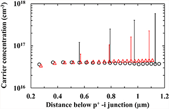
Figure 4. Carrier concentration in the devices as functions of distance below the p+-i junction for the 400 µm (red triangles) and the 200 µm (black circles) devices at 20 °C (293 K), taking into account the empty package capacitance (1.29 pF). For clarity, error bars are displayed in five data-point intervals, and the negative error bars have been removed.
Download figure:
Standard image High-resolution image3.2. Measurements of detector current as a function of applied bias
The dark currents of both devices were measured as functions of applied forward and reverse bias using a Keithley 6487 Voltage Source/Picoammeter; the procedure followed was as per the capacitance measurements. Figure 5(a) presents the measured forward current as a function of applied forward bias and figure 5(b) presents the measured reverse leakage current as a function of applied reverse bias for both the 200 µm and 400 µm devices.
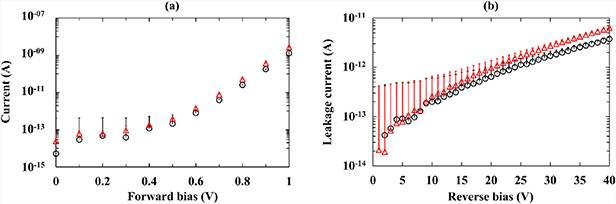
Figure 5. Current as a function of applied forward bias (a) and applied reverse bias (b), for the 400 µm device (red triangles) and the 200 µm device (black circles) at 20 °C (293 K). The negative error bars have been removed for clarity.
Download figure:
Standard image High-resolution imageThe leakage current was measured to be 3.7 pA ± 0.4 pA and 6.3 pA ± 0.4 pA for the 200 µm and 400 µm devices respectively, at the maximum applied reverse bias (40 V). The uncertainties associated with the current measurements were dominated by the uncertainty associated with the Keithley 6487 Voltage Source/Picoammeter. Assuming the electric field strength, Ef, was uniform and across only the depleted region (implying Ef = 345 kV cm−1 for the 200 µm device and Ef = 361 kV cm−1 for the 400 µm device, at 40 V) it was expected that the photodiodes were operating in the avalanche regime.
The leakage current density, JR, of the devices was calculated using the measured leakage current and is presented in figure 6. The leakage current density was calculated to be 11.9 nA cm−2 ± 1.3 nA cm−2 for the 200 µm device and 5.0 nA cm−2 ± 0.3 nA cm−2 for the 400 µm device at the maximum reverse bias (VR = 40 V; Ef = 345 kV cm−1 for the 200 µm device and Ef = 361 kV cm−1 for the 400 µm device (assuming Ef was uniform and across only the depleted region)). The difference in measured leakage current density between the two devices suggested that the leakage current did not scale with junction area. This was attributed to a non-negligible surface leakage current component, possibly due to the devices being unpassivated, in addition to possible differences in contact deposition and wire bonding [12].
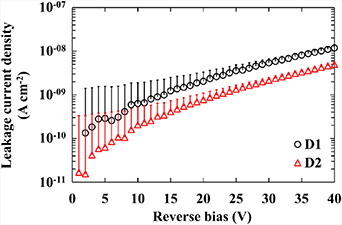
Figure 6. Leakage current density for the 200 µm device (black circles) and the 400 µm device (red triangles) as a function of reverse bias, at 20 °C (293 K). The negative error bars have been removed for clarity.
Download figure:
Standard image High-resolution imageFor AlxGa1-xAs (x > 0) x-ray photodiodes, the best (lowest) leakage current density previously reported at room temperature was 2.2 nA cm−2, at Ef = 100 kV cm−1 [33]. At the same Ef (equivalent to 5 V reverse bias for the current detectors, assuming Ef was uniform and across only the depleted region), the Al0.6Ga0.4As devices had leakage current densities of 0.3 nA cm−2 ± 1.3 nA cm−2 for the 200 µm device and 0.1 nA cm−2 ± 0.3 nA cm−2 for the 400 µm diameter device, thus the present detectors have much lower leakage current densities. The reported leakage current densities were also lower than recently studied GaAs devices: at 20 °C (293 K) and Ef = 50 kV cm−1, a 200 µm diameter GaAs device with a 10 µm i layer was measured to have a 6 nA cm−2 ±1 nA cm−2 leakage current density [34]. At the same Ef (equivalent to 2 V applied reverse bias for the present devices), the Al0.6Ga0.4As devices had leakage current densities of 0.1 nA cm−2 ±1.3 nA cm−2 for the 200 µm device and 1.5 pA cm−2 ±0.3 nA cm−2 for the 400 µm device. As previously mentioned, the difference in measured leakage current density between the two investigated devices was attributed to a non-negligible surface leakage current component, in addition to possible differences in contact deposition and wire bonding [12].
4. Photon counting x-ray spectroscopy
4.1. Experimental measurements and determination of the spectrometers' energy resolutions
The Al0.6Ga0.4As p+-i-n+ photodiodes were connected to a low-noise charge-sensitive custom-made preamplifier, similar in design to that of [35], each in turn. The output of the preamplifier was then connected to a shaping amplifier (Ortec 572A) whose output was digitised by a multi-channel analyser (Ortec 927). An 55Fe x-ray (Mn Kα = 5.9 keV; Mn Kβ = 6.49 keV) source (≈157 MBq) was positioned ≈4 mm above each Al0.6Ga0.4As detector in turn. The resultant spectrometers S200 (employing the 200 µm diameter photodiode) and S400 (employing the 400 µm diameter photodiode) were characterised. Each spectrometer was installed inside a TAS Micro MT environmental chamber to maintain an operating environment temperature of 20 °C (293 K). The environmental chamber was left for 1 h at this temperature to allow thermal equilibrium to be reached. To monitor temperature equilibrium between the environmental chamber and the spectrometer, a thermocouple was positioned close to the spectrometer. In order to reduce humidity related effects, the environmental chamber was purged with N2 (<5% relative humidity) throughout the measurements.
The shaping amplifier shaping time constant, τ, was kept at 2 µs throughout the measurements such that direct comparisons could be made between spectra. This shaping time was the optimal shaping time available from the Ortec 572 A shaping amplifier (i.e. that which minimised the combination of the white series and white parallel noise contributions). The shaping time was selected for this purpose rather than for optimising the maximum count rate of the system. Since the two detectors had different active areas, the live time limits of each spectrum was set differently: 1500 s for S200 spectra; 800 s for S400 spectra. For S200, spectra were accumulated with the detector operated at reverse biases of 0 V to 40 V in 2 V steps. For S400, spectra were accumulated with the detector operated at reverse biases of 30 V to 40 V in 2 V steps, since at lower reverse biases (<30 V), the photopeak could not be deconvolved from the so called zero energy noise peak.
The 55Fe x-ray spectra obtained with each spectrometer can be seen in figure 7. For clarity, not all spectra obtained are plotted; instead, a number of reverse biases have been selected to show the change in spectroscopic response. The form of response is consistent with an avalanche photodiode; this is further exemplified by plotting the change in main (largest) photopeak centroid position (corrected for changes in zero energy noise peak position) as a function of applied detector reverse bias, figure 8. Al0.8Ga0.2As avalanche x-ray photodiodes have been reported previously [25, 32, 36–38], but this is the first report of Al0.6Ga0.4 As avalanche x-ray photodiodes. The secondary peak observed on the left hand side of the primary peak is discussed in section 4.2.

Figure 7. Accumulated 55Fe x-ray spectra obtained with spectrometer S200 (a) and spectrometer S400 (b). All spectra were accumulated at the same shaping time (2 µs) and at constant temperature (20 °C, 293 K). The different peaks are distinguished and explained in section 4.2.
Download figure:
Standard image High-resolution image
Figure 8. The position of the main (largest) 55Fe x-ray photopeak in each spectrum (corrected for any changes in zero energy noise peak position) for spectrometer S200 (circles) and spectrometer S400 (triangles) as a function of applied detector reverse bias.
Download figure:
Standard image High-resolution imageGaussian fitting was applied to the main photopeak assuming that it was composed of 5.9 keV (Mn Kα) and 6.49 keV (Mn Kβ) x-rays from the 55Fe x-ray source; the relative emission ratio of these x-rays (Mn Kα = 0.879; Mn Kβ = 0.122 [39]), and the relative detector quantum efficiency at these energies (see figure 3), were taken into account.
Energy calibration of each spectrum was achieved by using the zero energy noise peak and fitted 5.9 keV peak positions, assuming a linear variation of detected charge with energy. The energy resolution (FWHM at 5.9 keV) was determined for all spectra. Examples of the spectra with the Gaussians fitted are shown in figure 9 for S200 with detector applied biases of 10 V (figure 9(a)) and 38 V (figure 9(b)). Figure 10 shows the determined FWHM at 5.9 keV of the S200 and S400 spectrometers as functions of applied detector reverse bias.
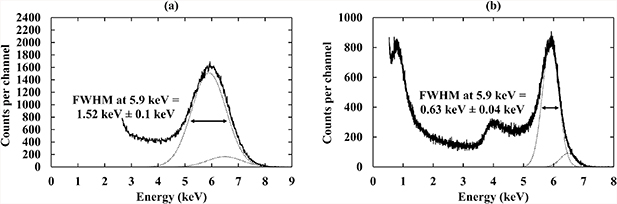
Figure 9. Spectrum accumulated with spectrometer S200 at an applied detector reverse bias of 10 V (a) and 38 V (b), when exposed to an 55Fe x-ray source. The dotted lines are the fitted 5.9 keV (Mn Kα) and 6.49 keV (Mn Kβ) peaks.
Download figure:
Standard image High-resolution image
Figure 10. Determined energy resolution (FWHM at 5.9 keV) for spectrometer S200 (circles) and S400 (triangles) as a function of applied detector reverse bias.
Download figure:
Standard image High-resolution imageThe measured energy resolution (FWHM at 5.9 keV) of the presently reported devices was better than any previously reported AlxGa1-xAs x-ray photodiode at room temperature. For non-avalanche mode AlxGa1-xAs x-ray detectors, the best energy resolution previously reported was 760 eV FWHM at 5.9 keV at 20 °C (293 K) [23], using square, 200 µm by 200 µm, 3 µm i layer, Al0.2Ga0.8As p+-i-n+ x-ray photodiodes. For avalanche mode AlxGa1-xAs x-ray detectors, excluding separate absorption and multiplication region (SAM) avalanche photodiodes, the best previously reported energy resolution was 1.21 keV FWHM at 5.9 keV at room temperature [25], using an Al0.8Ga0.2As p+-p–n+ circular device, 200 µm in diameter. Similar energy resolutions have been reported for GaAs-Al0.8Ga0.2As SAM avalanche photodiodes (1.08 keV FWHM at 5.9 keV at room temperature [37]). The presently reported energy resolution was also better than has been reported in recent studies of other wide bandgap materials, such as Al0.52In0.48P; non-avalanche mode, 200 µm diameter, 2 µm i layer, Al0.52In0.48P p+-i-n+ circular mesa x-ray photodiodes were reported to have an energy resolution of 930 eV FWHM at 5.9 keV [12]. Avalanche mode, 200 µm diameter, Al0.52In0.48P p+-i-p–n+ circular mesa x-ray photodiodes were reported to have an energy resolution of 682 eV FWHM at 5.9 keV [11]. At optimal operating conditions, and at 20 °C (293 K), the presently reported spectrometers had a measured energy resolution of 630 eV ± 40 eV (at VR = 38 V) and 730 eV ± 50 eV (at VR = 40 V) FWHM at 5.9 keV, for S200 and S400 respectively. It should be noted that the reported energy resolutions, when compared to those measured for state-of-the-art Si detectors and GaAs detectors, are still relatively modest. For example, a GaAs 5 × 5 diode array (40 µm i layer), when connected to ultra-low-noise front end electronics, was reported to have an energy resolution of 266 eV FWHM at 5.9 keV at room temperature [4]. A Silicon Drift Detector (SDD) coupled to ultra-low-noise CMOS readout electronics was reported to have an energy resolution of 141 eV FWHM at 5.9 keV at room temperature [40]. A Si depleted p channel field effect transistor (DEPFET) detector was reported to have an energy resolution of 134 eV FWHM at 5.9 keV at room temperature [41].
The minimum energy cut-off was determined to be ≈2 keV at the optimal operating conditions for both S200 and S400. As a comparison, a minimum energy cut-off of 1.5 keV and 170 eV was estimated at room temperature using a GaAs 5 × 5 diode array [4] and Silicon Drift Detector (SDD) [40] respectively, when coupled to ultra-low-noise readout electronics. It should be noted that, aside from the quality of the detector, the use of low noise readout electronics plays a significant part in improving (reducing) the energy resolution and minimum energy cut-off of an x-ray spectrometer.
4.2. Origin of the secondary peak in the obtained x-ray spectra
As seen in figure 7, at high detector reverse bias (⩾34 V for S200; ⩾36 V for S400) a secondary peak was present at the low energy side of the main photopeak. The separation between the secondary and main peak increased as the detector reverse bias was increased. Figure 11 shows how the positions of the main and secondary peaks change as functions of applied detector reverse bias for both spectrometers. A third peak, close to the low energy threshold, was also present in spectra obtained with S200 at detector reverse biases ⩾38 V, and with S400 at a detector reverse bias of 40 V. The third peak was hypothesised to be from Al Kα (1.49 keV [42]) x-rays from detector self-fluorescence; these x-rays became detectable due to improvement in the low energy x-ray performance of the spectrometers at high detector reverse biases as a consequence of the avalanche multiplication.

Figure 11. The position of the main (circles) and secondary (diamonds) 55Fe x-ray photopeak in each spectrum (corrected for any changes in zero energy noise peak position) as a function of applied detector reverse bias for spectrometer S200 (a) and spectrometer S400 (b).
Download figure:
Standard image High-resolution imagePeaks similar to the secondary peak seen here have also been recorded with SAM APDs made from GaAs-Al0.8Ga0.2As [37] and Al0.52In0.48P [11]. In those cases, the secondary peaks were attributed to holes, created in the n region(s) of the detectors below the avalanche layer, receiving the maximum possible hole initiated avalanche multiplication as they benefitted from the full width of the avalanche region. However, other experimental and theoretical work on Al0.8Ga0.2As p+-p–n+ x-ray APDs indicated that pure hole initiated multiplication of this type played no significant part in spectrum formation due to loss of the holes (e.g. by recombination) before those charge carriers could reach the avalanche region [25, 32].
Furthermore, in the case of the SAM APDs described in [11, 37], the main peak in each spectrum was formed by electrons. These were created by photons absorbed in a low doped absorption region and subsequently transported to a relatively thin avalanche region; they underwent maximum pure electron multiplication since they benefitted from the whole of the width of the avalanche region. This is a different mechanism of formation of main peak than was present in the p+-p–n+ APDs [32, 38], where the main peak was formed from both electrons and holes which were created within the p- layer of the detector. This p- layer was also the avalanche region of that device and consequently charge carriers created there received a mixed multiplication, which would normally be dependent on the photon absorption position within the layer. However, the doping profile in the particular case of the previously reported p+-p–n+ device was said to be such as to compensate for this position dependence [25, 32, 38]; a simulated spectrum showing the morphology which would have been expected without this special doping profile was presented as figure 3 in [32].
Those earlier reported p+-p–n+ APDs did show an additional peak but this was at the right hand (high energy) side of the main peak. This additional peak was shown to be a consequence of electrons generated by photons absorbed within the p+ region of the detector diffusing towards the p− layer and subsequently receiving the maximum pure electron initiated multiplication. It should be noted that, in that case, the only electrons that reached the p− layer were those created within 0.16 µm of the p+−p− junction. Thus, in that case, the 0.16 µm of material close to the p+−p− junction acted analogously to the absorption region in the SAM APDs. In the case of the present devices, which are p+−i−n+ APDs rather than SAM APDs, the absorption and multiplication regions are not separate. Consequently, a spectrum morphology as per figure 3 of [32] was expected to be obtained, assuming there was no contribution from holes created in the device's n+ layer or the non-depleted portion of its i layer. If there was a contribution from holes created in those regions, the spectrum expected to be accumulated with the present Al0.6Ga0.4As devices would be similar to figure 3 of [32] but with a further additional peak (akin to that from the p+−p–n+ device's p+ layer) but at the low energy side of the primary (p- layer) peak.
However, the morphologies of the spectra obtained with the present devices appear to be more similar to those obtained with the SAM APDs than from the p+-p–n+ APD spectra and earlier modelling. A superficial similarity between the current spectra (e.g. Figure 9(b)) and figure 3 of [32] is noted, but in the present case the depletion region is thicker (1.16 µm ± 0.08 µm for the 200 µm device and 1.11 µm ± 0.02 µm for the 400 µm device at VR = 40 V) than the p+ region (0.5 µm), and both are relatively thin. Consequently, even if the whole of the p+ was active, the number of counts from the depletion region should be much greater than the number from the p+ region. However, the spectrum shape does not indicate this: the number of counts within the saddle between the main and secondary peaks is relatively small compared with the number of counts in the main peak. Consequently, the origin of the spectra morphologies obtained with the present devices is currently unknown.
4.3. Impact ionisation coefficients and multiplication factors
As shown by figures 7, 8 and 11, the spectroscopic response of the 200 µm diameter device and 400 µm diameter device changed as a function of detector reverse bias in a manner consistent with an avalanche photodiode. Before determining the apparent multiplication factors, it should be noted that through extensive characterisation, the charge output of the low-noise charge-sensitive custom-made preamplifier used in this work has been found to be sensitive to changes in capacitance at its input (⩾0.2 pF); where a reduction in capacitance at the input (e.g. reduction in detector capacitance) caused an increase in output voltage. Since the capacitance of the 200 µm diameter device and 400 µm diameter device decreased as a function of detector reverse bias within the investigated range (see figure 1), the change in spectroscopic response due to the change in capacitance must be understood before the apparent gain from avalanche multiplication can be calculated.
Since the non-avalanche photopeak of the 400 µm diameter device could not be separated from the so called zero energy noise peak, only the 200 µm diameter device was considered. The 200 µm diameter device was coupled to the same preamplifier as used in section 4.1. A Berkeley Nucleonics Corporation model BH-1 tail pulse generator was coupled to the preamplifier test signal input, to quantify the change in apparent conversion gain of the preamplifier resulting from a change in applied bias (and consequently a change in capacitance) of the connected detector. Spectra were acquired whilst operating the detector at reverse biases from 10 V (assumed to be operating in non-avalanche mode) to 40 V in 10 V steps at a shaping time, τ, and live time, of 2 µs and 300 s, respectively, at 20 °C (293 K). The experiment was performed at four different pulse generator amplitudes (test signal input charges) in order to ensure there was no unexpected variation of preamplifier response as a function of pulse generator amplitude; no variation in this regard was detected.
The position of the pulser peak (corrected for any changes in zero energy noise peak position) was found to increase by 17% ± 1% as VR increased from 10 V to 40 V. Previous investigations of the custom-made preamplifier found no appreciable change in spectral response as a function of detector current for currents ⩽6 pA. Consequently, the change in pulser peak position reported here was attributed solely to the change in detector capacitance. The mean change in conversion factor per unit capacitance was measured to be 6.7% pF−1 ± 0.4% pF−1 (rms deviance). The change in conversion factor due to change in capacitance was subtracted from the measured peak positions (see figure 11) and has been plotted in figure 12.
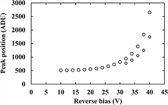
Figure 12. The position of the main (circles) and secondary (diamonds) 55Fe x-ray photopeak in each spectrum (corrected for any changes in detector capacitance and zero energy noise peak position) as a function of applied detector reverse bias for spectrometer S200.
Download figure:
Standard image High-resolution imageThe apparent multiplication factor, M, was calculated for the spectrometer S200 by calculating the ratio between the fitted primary 5.9 keV peak position at each bias and the fitted primary 5.9 keV peak position at unity gain (M = 1, observed at an applied detector reverse bias of 10 V, given that the fitted primary 5.9 keV peak position did not change beyond the measurement uncertainty until an applied detector reverse bias of 14 V). The same procedure was used for calculating the secondary 5.9 keV peak apparent multiplication factor, assuming unity gain at 10 V applied reverse bias. The apparent multiplication factor for both peaks is shown in figure 13.
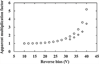
Figure 13. Apparent multiplication factor for the main (circles) and secondary (diamonds) 55Fe x-ray photopeak in each spectrum (corrected for any changes in detector capacitance and zero energy noise peak position) for spectrometer S200 as a function of detector reverse bias.
Download figure:
Standard image High-resolution imageApparent multiplication factors of 5.20 and 3.43 were measured at an applied detector reverse bias of 40 V for the primary and secondary 55Fe x-ray photopeaks, respectively. The tertiary peak mentioned in section 4.2, appeared to have the same avalanche multiplication as the secondary peak, assuming that the third peak is indeed a result of Al Kα x-ray fluorescence. The multiplication factors were larger than expected; at a detector reverse bias of 40 V, and assuming that the electric field strength was uniform and across only the depleted region (see figure 3(a)), a maximum pure electron multiplication factor, Me, of 1.22, and a maximum pure hole multiplication factor, Mh, of 1.18 were calculated given the material's accepted impact ionization coefficients [43]. Given this, the measured relative positions of the peaks were considered in an attempt to establish if there was an alternative 'effective' field strength that would explain the results and maintain the accepted impact ionization coefficients. Two approaches were considered: one starting from the position of the primary peak; and one starting from the position of the secondary peak.
The first approach calculated the expected multiplication of the secondary peak given the apparent multiplication of the primary peak. Thus, it was considered that the primary peak may be a consequence of maximum pure electron multiplication; if this was the case then perhaps the secondary peak was from either maximum pure hole multiplication or mixed multiplication. Given the material's accepted impact ionization coefficients [43], if the primary peak's apparent multiplication factor of 5.20 was a consequence of maximum pure electron multiplication, then the secondary peak's multiplication, M, would be 4.66 if it was a result of maximum pure hole multiplication, or 4.66 < M < 5.20 if it was a consequence of mixed multiplication. Since the measured multiplication factor of the secondary peak was 3.43, neither explanation in the first case fits the measurements.
The second approach calculated the expected multiplication of the primary peak given the apparent multiplication of the secondary peak. Thus, correspondingly with the first case, if the secondary peak's measured multiplication (3.43) was a consequence of maximum pure hole multiplication then, given the accepted impact ionization coefficients, a primary peak multiplication of 3.80 was expected if it was a consequence of maximum pure electron multiplication, whereas 5.20 was measured experimentally.
Since both approaches indicated that the measured multiplication factors could not be explained by the accepted ratio between the electron and hole impact ionization coefficients, it was considered that it may be informative to calculate the apparent impact ionization coefficients implied by the experimental multiplication factor measurements. With the assumption that the primary peak's multiplication was a result of maximum pure electron multiplication and the secondary peak's multiplication was a result of maximum pure hole multiplication, the apparent impact ionization coefficients were calculated and are presented in figure 14. Since the secondary peak was only clearly resolved at reverse biases ⩾32 V, this is the minimum reverse bias for which the apparent impact ionization coefficients could be determined. The values were calculated by assuming the McIntyre local model [44], such that


Figure 14. Apparent ionization coefficients for electrons, α, (circles), and holes, β, (diamonds) for spectrometer S200 as a function of detector reverse bias. The electric field strength, assuming it was uniform and across only the depleted region, has been plotted.
Download figure:
Standard image High-resolution imagewhere α is the electron impact ionization coefficient, Me is the maximum pure electron multiplication factor, Mh is the maximum pure hole multiplication factor, and W is the depletion width, and
where β is the hole impact ionization coefficient [25].
The apparent electron and hole impact ionization coefficients were substantially greater than the generally accepted values reported by Plimmer et al [43]. For example, at a detector reverse bias of 40 V (Ef = 345 kV cm−1), apparent ionisation coefficients α = 8513 and β = 4930 were measured, whereas the accepted ionisation coefficients at this field strength are α = 930 and β = 742 [43]. The origin of this discrepancy is currently unknown.
5. Electron-hole pair creation energy measurements
In order to determine the electron-hole pair creation energy, ω, at 25 °C ± 1 °C (298 K ± 1 K) for the presently reported detector material, Al0.6Ga0.4As, the same method used to determine ω in SiC [1] and GaAs [45], using a Si reference detector, as well as Al0.2Ga0.8As [19], Al0.8Ga0.2As [46], Al0.52In0.48P [47], and In0.5Ga0.5P [48], using a GaAs reference detector, was followed. Care was taken to ensure that avalanche multiplication did not affect the measurement. The layer structure of the well characterised 200 µm diameter GaAs p+-i-n+ x-ray photodiode [49], which was used as a reference device, is presented in table 2.
Table 2. GaAs reference diode structure details.
| Material | Dopant | Dopant type | Thickness (nm) | Doping density (cm−3) |
|---|---|---|---|---|
| GaAs | C | p | 10 | 1 × 10¹⁹ |
| GaAs | C | p | 500 | 2 × 10¹⁸ |
| GaAs | i | 10 000 | Undoped | |
| GaAs | Si | n | 1000 | 2 × 10¹⁸ |
| GaAs n+ substrate |
The presently reported 200 µm Al0.6Ga0.4As device and the 200 µm GaAs reference device were connected in parallel to a low-noise charge-sensitive custom-made preamplifier, similar to that used in section 4. An 55Fe x-ray source was placed, in turn, atop each device, ensuring minimal disruption to the detector/preamplifier system [50]. For the duration of the measurement, the housing in which the detectors and preamplifier were installed was purged continually with dry N2 (<5% relative humidity) in order to eliminate any humidity related effects [7]. For each spectrum, the live time limit was 2000 s. X-ray spectra were obtained with the GaAs reference detector at its optimum reverse bias of 5 V, and the Al0.6Ga0.4As photodiode at a reverse bias of 10 V. This reverse bias was chosen in order to ensure the detector was operating in non-avalanche mode (avalanche did not occur until an applied detector reverse bias of 14 V, see figure 13). The shaping time was set to 10 µs (the optimal shaping time for the dual detector configuration). The temperature of the detector was measured and remained at 25 °C ± 1 °C (298 K ± 1 K) for the duration of the experiment. Although the experimental system was identical to that of [19, 47, 48], where the detectors were illuminated individually, it should be noted that the experimental system differed slightly from that used in [1, 45, 46]. This adjustment used in the present case (and in [19, 47, 48].) was used to prevent additional distortion (undershoot) from the preamplifier output caused by two detectors being connected in parallel [50]; see [19] for further details. Although measurements obtained in this manner can result in input JFET or detector leakage current instability, it was found that, through initial measurements of these parameters, no such effects were present for the duration of the experiment.
Gaussian fitting was applied to the obtained 55Fe spectra with the Al0.6Ga0.4As and GaAs devices, as shown in figure 15. As per section 4.1, the detectors' relative detection efficiencies for the 5.9 keV (Mn Kα) and 6.49 keV (Mn Kβ) photons, and the accepted emission ratio [39], were taken into account. Figure 15 presents spectra accumulated with the Al0.6Ga0.4As and GaAs devices when illuminated separately but connected in parallel; the spectra have been normalised in terms of peak height and are presented within the same figure. The so called zero energy noise peak position and 5.9 keV Mn Kα peak position obtained with the GaAs photodiode, together with the accepted ωGaAs value (4.184 eV ± 0.025 eV [45]), were used to charge calibrate the spectra. The dotted and dashed lines of figure 15 correspond to the fitted Mn Kα and Mn Kβ peaks for the Al0.6Ga0.4As and GaAs devices respectively.
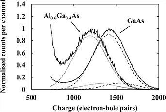
Figure 15. Accumulated 55Fe spectra at 25 °C ± 1 °C (298 K ± 1 K) for each detector (solid line as indicated). The Al0.6Ga0.4As device was operated at a reverse bias of 10 V, with a shaping amplifier shaping time of 10 µs. The GaAs detector was operated at a reverse bias of 5 V, with a shaping amplifier shaping time of 10 µs. The devices were illuminated separately in turn, but connected in parallel. The spectra have been normalised using their associated centroid peak heights. The 5.9 keV and 6.49 keV fitted Gaussian peaks of the Al0.6Ga0.4As device (dotted lines) and the GaAs reference device (dashed lines) have been plotted.
Download figure:
Standard image High-resolution imageThe difference in photopeak position of the Al0.6Ga0.4As and GaAs devices, as shown in figure 15, is a consequence of the difference in electron-hole pair creation energy for each material [46]. Therefore, assuming complete charge collection, the electron-hole pair creation energy of Al0.6Ga0.4As, ωAlGaAs, can be calculated by,
where NGaAs and NAlGaAs are the average numbers of created charge carriers for GaAs and Al0.6Ga0.4As respectively.
Equation (5) and the accepted value of ωGaAs (4.184 eV ± 0.025 eV [45]) were used to calculate ωAlGaAs. It was found to be 4.97 eV ± 0.12 eV at 25 °C ± 1 °C (298 K ± 1 K).
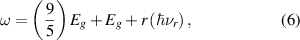
Different radiation types have been used to better understand the effect of the physical characteristics of semiconductors to their corresponding electron-hole pair creation energy [51]. According to Klein [52], the empirical relationship between the bandgap energy and the electron-hole pair creation energy of semiconducting material, can be expressed as,
where (9/5) e.g. is the residual kinetic energy, e.g. is the bandgap, and r(ℏνr) is the optical phonon losses whose value, according to Klein, is within the range 0.5 eV ⩽ r(ℏνr) ⩽ 1.0 eV [52]. The bandgap energies of many materials and their determined electron-hole pair creation energies was presented by [22, 52], and subsequently by [53]. Identified in this data set was a so called main Klein function branch (ω = (14/5)Eg + 0.6). However, some materials, including 4H-SiC, AlN, PbI2, HgI2, and diamond, have been reported to be displaced from this main branch, instead residing on an apparent secondary Klein function branch, where r(ℏνr) = −1.5 eV. This secondary branch cannot be explained by the Klein model since r(ℏνr) < 0 would be unphysical. Furthermore, some years ago, it was also found that the electron-hole pair creation energy of Al0.8Ga0.2As was situated between the two supposed branches [24, 46], adding additional weight to the conclusion that the Klein model is unphysical.
Additional complexity arises since the electron-hole pair creation energy values compiled by [22, 52, 53]. are not all reported at the same temperature, nor did they necessarily all use the same radiation type or quanta energy. As the electron-hole pair creation energy is temperature dependent, comparisons between materials should be made at a standard temperature. Furthermore, there has been variation between values reported for materials when different radiation types are used, as acknowledged by Klein [52], and it is thought that there may be a dependence of electron-hole pair creation energy on energy of the radiation quanta used in the measurement—although the dependence is thought to be relatively small except near absorption edges [54]. A further complication is that accurate measurements of electron-hole pair creation energy require high quality material; consequently, there is a tendency for the apparent electron-hole pair creation energy to reduce as materials mature and qualities improve. It is also experimentally challenging to perform the measurement, requiring a very low noise preamplifier and high levels of experimental technique to ensure that subtle changes close to the input JFET of the preamplifier do not influence the measurement. All of these things call into question the reliability of both the Klein model and the data used to imply that model.
As such, great care must be taken to include only measurements of which the provenance is certain when trying to establish the relationship between bandgap energy and electron-hole pair creation energy. Therefore, having excluded the questionable measurements, Barnett et al plotted the electron-hole pair creation energy of Al0.8Ga0.2As [24, 46] together with Si, Ge, and GaAs data reported by Bertuccio and Maiocchi [45] as a function of bandgap, and demonstrated a different relationship than expected from the Klein relationship. The measurement of Al0.8Ga0.2As was critical in this since it was at that stage the only measurement of the four which was sufficiently displaced from either Klein branch as to conclusively indicate a different relationship. Subsequently, this Bertuccio–Maiocchi–Barnett (BMB) relationship was used to predict (correctly within the associated uncertainties) the electron-hole pair creation energies of Al0.2Ga0.8As [19], Al0.52In0.48P [47], and In0.5Ga0.5P [48], and the experimental measurements of these materials' electron-hole pair creation energies were then used to refine the BMB relationship, such that

where all the parameters have been previously defined. From this it can be seen that equation (7) also correctly predicts an electron-hole pair creation energy of 5.02 eV ± 0.16 eV for Al0.6Ga0.4As at room temperature, which agrees with the experimental value obtained in the current work (4.97 eV ± 0.12 eV). Adding this new value to the dataset, the BMB relationship was refined to,

The dataset including the new value for Al0.6Ga0.4As is presented in figure 16.

Figure 16. Electron-hole pair creation energies for Al0.52In0.48P, Al0.8Ga0.2As, Al0.6Ga0.4As, In0.5Ga0.5P, Al0.2Ga0.8As, GaAs, Si, and Ge, as a function of bandgap energy at ≈300 K.
Download figure:
Standard image High-resolution image
Strictly speaking, despite the fit of the new datum within the set, the value of the electron-hole pair creation energy determined for Al0.6Ga0.4As should be considered as an upper limit of the parameter in this material, since it cannot be guaranteed that the collection of the charge generated was perfect in its totality.
To demonstrate the inadequacy of the Klein relationship to accurately model the bandgap energy as a function of electron-hole pair creation energy, it is informative to consider its predictions of the Al0.6Ga0.4As electron-hole pair creation energy. If Al0.6Ga0.4As were to rest either on the so called main Klein function branch or secondary Klein function branch, values of ωAlGaAs = 6.28 eV and ωAlGaAs = 4.18 eV would have been expected, respectively. However, neither of these values agree with the experimentally measured value (4.97 eV ± 0.12 eV). Therefore, Al0.6Ga0.4As is another material for which the BMB relationship accurately predicted the electron-hole pair creation energy, whilst the Klein relationship did not.
6. Conclusions and further work
Custom-made Al0.6Ga0.4As p+-i-n+ circular mesa spectroscopic x-ray avalanche photodiodes (2 µm i layer) of different diameters (one 200 µm device and one 400 µm device), were investigated for their response to x-ray illumination by an 55Fe x-ray (Mn Kα = 5.9 keV; Mn Kβ = 6.49 keV) source, and their electrical properties characterised, at 20 °C (293 K). The electron-hole pair creation energy of Al0.6Ga0.4As (=4.97 eV ± 0.12 eV) at 25 °C ± 1 °C (298 K ± 1 K) was also measured, using the 200 µm diameter device.
For both devices, the measured leakage currents were improved relative to that previously reported for AlxGa1-xAs x-ray detectors at room temperature (2.2 nA cm−2, at Ef = 100 kV cm−1 [33]), where leakage current densities of 0.3 nA cm−2 ± 1.3 nA cm−2 for the 200 µm device and 0.1 nA cm−2 ± 0.3 nA cm−2 for the 400 µm device were measured at Ef = 100 kV cm−1. At the maximum applied reverse bias (VR = 40 V; Ef= 345 kV cm−1 for the 200 µm device and Ef = 361 kV cm−1 for the 400 µm device), the leakage current density was measured to be 11.9 nA cm−2 ± 1.3 nA cm−2 for the 200 µm device and 5.0 nA cm−2 ± 0.3 nA cm−2 for the 400 µm device. The difference in leakage current density between the 200 µm diameter device and 400 µm diameter device indicated a significant surface leakage current contribution [12].
Measurements of the devices' capacitances suggested that the depletion width of the 200 µm device increased from 0.26 µm ± 0.02 µm at 0 V reverse bias to 1.16 µm ± 0.08 µm at 40 V reverse bias, and that the depletion width of the 400 µm device increased from 0.28 µm ± 0.02 µm at 0 V reverse bias to 1.11 µm ± 0.02 µm at 40 V reverse bias. Both devices were not fully depleted at 40 V reverse bias, but greater magnitude reverse biases were not investigated in order to ensure that the devices had their leakage currents kept to <1 nA in order to prevent damage.
The x-ray detection response of both Al0.6Ga0.4As detectors was characterised at 20 °C (293 K). Each photodiode was connected to an identical low-noise charge-sensitive custom-made preamplifier, in turn, and onwards to standard x-ray spectrometer electronics. The best energy resolution (FWHM at 5.9 keV) was 630 eV ± 40 eV for the 200 µm diameter device, obtained at an operating reverse bias of 38 V, and 730 eV ± 50 eV for the 400 µm diameter device, obtained at an operating reverse bias 40 V. The measured energy resolution (FWHM at 5.9 keV) of the presently reported devices was better than any previously reported AlxGa1-xAs x-ray photodiodes at room temperature (0.76 keV FWHM at 5.9 keV at 20 °C (293 K) [23]) and comparable to that measured in recent studies of other wide bandgap III–V materials, such as Al0.52In0.48P (e.g. 682 eV FWHM at 5.9 keV [11]). Although the energy resolution reported is still modest in comparison to those measured using state-of-the-art Si detectors and state-of-the-art readout electronics (e.g. 134 eV FWHM at 5.9 keV [41]).
The spectroscopic response of the 200 µm device and the 400 µm device changed as a function of applied reverse bias in a manner consistent with an avalanche photodiode. At high detector reverse bias, secondary and tertiary peaks were present at the low energy side of the main photopeak (see figure 8). The third peak was hypothesised to be from Al Kα (1.49 keV [42]) x-rays from detector self-fluorescence (see section 4.2). The secondary and main peak were both from the combination of the emissions from the 55Fe x-ray (Mn Kα = 5.9 keV; Mn Kβ = 6.49 keV) source. The morphologies of the spectra obtained with the present devices appeared similar to those obtained with SAM APDs made from GaAs-Al0.8Ga0.2As [37] and Al0.52In0.48P [11], in those cases, the secondary peaks were attributed to holes created in the n region(s) of the detectors below the avalanche layer, receiving the maximum possible hole initiated avalanche multiplication. Similarly, in those cases, the main peaks were attributed to electrons created in the p region(s) of the detectors above the avalanche layer, receiving the maximum possible electron initiated avalanche multiplication. Given the presently reported devices structure however, this was not expected. Even if the whole of the p+ was active, the number of counts from the depletion region should be much greater than the number from the p+ region. Consequently, the origin of the spectra morphologies is currently unknown.
The apparent multiplication factors of the primary and secondary 55Fe x-ray photopeaks for the 200 µm Al0.6Ga0.4As device based spectrometer were measured as a function of increasing applied reverse bias. Values of 5.20 and 3.43 were measured at 40 V applied reverse bias to the detector for the primary and secondary 55Fe x-ray photopeaks, respectively. The apparent impact ionization coefficients, α and β, were calculated assuming that the primary (and secondary) peaks corresponded to events which had received maximum pure electron (and maximum pure hole) initiated avalanche multiplication, respectively. With 40 V reverse bias (Ef = 345 kV cm−1) applied to the detector, apparent ionisation coefficients of α = 8513 and β = 4930 were calculated from the measurements.
The electron-hole pair creation energy for Al0.6Ga0.4As was measured to be 4.97 eV ± 0.12 eV at 25 °C ± 1 °C (298 K ± 1 K). This value agrees with the Bertuccio–Maiocchi–Barnett (BMB) relationship between bandgap energy and electron-hole pair creation energy, which predicted 5.02 eV ± 0.16 eV for Al0.6Ga0.4As at room temperature, prior to being refined by the new measurement. The new measurement demonstrates that Al0.6Ga0.4As is yet another material whose electron-hole pair creation energy is not predicted accurately by the Klein relationship. The main and secondary Klein branches predict Al0.6Ga0.4As would have an electron-hole pair creation energy of 6.28 eV or 4.18 eV, respectively.
Using the experimental measurement of the electron-hole pair creation energy in Al0.6Ga0.4As, the BMB relationship was refined such that

In future work, Monte Carlo modelling may be conducted in order to explain the origin and formation mechanisms of the measured photopeaks reported here. The presently reported Al0.6Ga0.4As p+-i-n+ spectroscopic x-ray photodiodes will be characterised as a function of temperature such that their performance over the temperature ranges expected of space science missions in which these devices are anticipated to find utility (e.g. exploration of the poles of Mercury, where surface temperatures reach 70 °C (343 K) [28]) can be assessed. A systematic study of a larger number of devices will follow as work progresses towards producing Al0.6Ga0.4As p+-i-n+ photodiode imaging arrays. AlxGa1-xAs of varying x will be studied such that the electron-hole pair creation energy dependence on bandgap energy, across the GaAs to AlAs range, can be mapped more completely.
Acknowledgments
This work was supported, in part, by the Science and Technology Facilities Council, UK; Grants ST/P001815/1 and ST/M004635/1. M.D.C.W. gratefully acknowledges funding from the University of Sussex, UK, in the form of a PhD scholarship. A.M.B. acknowledges funding from the Leverhulme Trust, UK, in the form of a 2016 Philip Leverhulme Prize. The authors are grateful to R. J. Airey and S. Kumar at the EPSRC National Centre for III-V Technologies for device fabrication.
Authors' data statement
Data underlying this work are subject to commercial confidentiality. The Authors regret that they cannot grant public requests for further access to any data produced during the study. However, the key findings are fully included within the article.