


Neuromorphic computing
With the ultimate aspiration of crafting an “artificial brain,” since the earliest stages of development, the fields of computer science and neurobiology have been intricately linked, as advances in each field have motivated reconsideration in the other.Reference Turing1,Reference von Neumann2 With the advancement of very large-scale integration (VLSI) frameworks, neuromorphic systems were introduced in the late 1980s to early 1990s as a methodology by which computers could better emulate the brain's natural processes, and thereby harness the associated advantages in power consumption and complexity of computation.Reference Mead3
In the intervening decades, much of the work toward a synthetic neural system has been focused in one of two directions. For the purpose of distinction, we will use the terms simulation and emulation to refer to two distinct processes. Simulation is the process by which phenomenon Aisreplicated phenomenologically with no regard to how the implementation may or may not mimic the original process. A familiar example comes from the world of Monte Carlo simulations, wherein the underlying physics need not be hard-coded into the simulation in order to accomplish something useful. On the other hand, emulation is the process by which phenomenon A is replicated with an eye toward reproducing the processes of A in the most faithful way possible. Consider, for example, the hardware limitations that are put in place by console designers in order to ensure backwards compatibility, thereby emulating an earlier generation of devices. Along similar lines, we can consider multiple avenues by which neural processes have been pursued in the past decades.
Inspired by the feed-forward nature of neural signals, artificial neural networks were initially designed to simulate neural signal processing by way of a high-level analogy between the functions being implemented within the algorithm and the weight-adapted operations performed along a neuron's length, as discussed in Reference 4 and shown in Figure 1.Reference Tang, Yuan, Shen, Wang, Rao, He, Sun, Li, Zhang, Li, Gao, Qian, Bi, Song, Yang and Wu4 As the available computational power increased with the progression of Moore's Law, great advances were made in the field of deep learning,Reference LeCun, Bengio and Hinton5 ranging from mastery of the game Go,Reference Silver, Huang, Maddison, Guez, Sifre, van den Driessche, Schrittwieser, Antonoglou, Pannershelvam, Lanctot, Dieleman, Grewe, Nham, Kalchbrenner, Sutskever, Lillicrap, Leach, Kavukcuoglu, Graepel and Hassabis6 speech recognition,Reference Hinton, Deng, Yu, Dahl, Mohamed, Jaitly, Senior, Vanhoucke, Nguyen, Sainath and Kingsbury7 face recognition,Reference Schroff, Kalenichenko and Philbin8 and machine translation,Reference Wu, Schuster, Chen, Le, Norouzi, Macherey, Krikum, Cao, Gao, Macherey, Klingner, Shah, Johnson, Liu, Kaiser, Gouws, Kato, Kudo, Kazawa and Stevens9 among others. The overwhelming majority of these advances have come almost exclusively due to the development of dedicated hardware optimized for the kinds of large-scale vector operations associated with these platforms, including graphic processing units (GPUs) and other custom designed application-specific integrated circuits (ASICs).Reference Jouppi, Young, Patil, Patterson, Agrawal, Bajwa, Bates, Bhatia, Boden, Borchers, Boyle, Cantin, Chao, Clark, Coriell, Daley, Dau, Dean, Gelb, Ghaemmaghami, Gottipati, Gulland, Hagmann, Ho, Hogberg, Hu, Hundt, Hurt, Ibarz, Jaffey, Jaworski, Kaplan, Khaitan, Killebrew, Koch, Kumar, Lacy, Laudon, Law, Le, Leary, Liu, Lucke, Lundin, MacKean, Maggiore, Mahony, Miller, Nagarajan, Narayanaswami, Ni, Nix, Norrie, Omernick, Penukonda, Phelps, Ross, Ross, Salek, Samadiani, Severn, Sitikov, Snelham, Souter, Steinberg, Swing, Tan, Thorson, Tian, Toma, Tuttle, Vasudevan, Walter, Wang, Wilcox and Yoon10
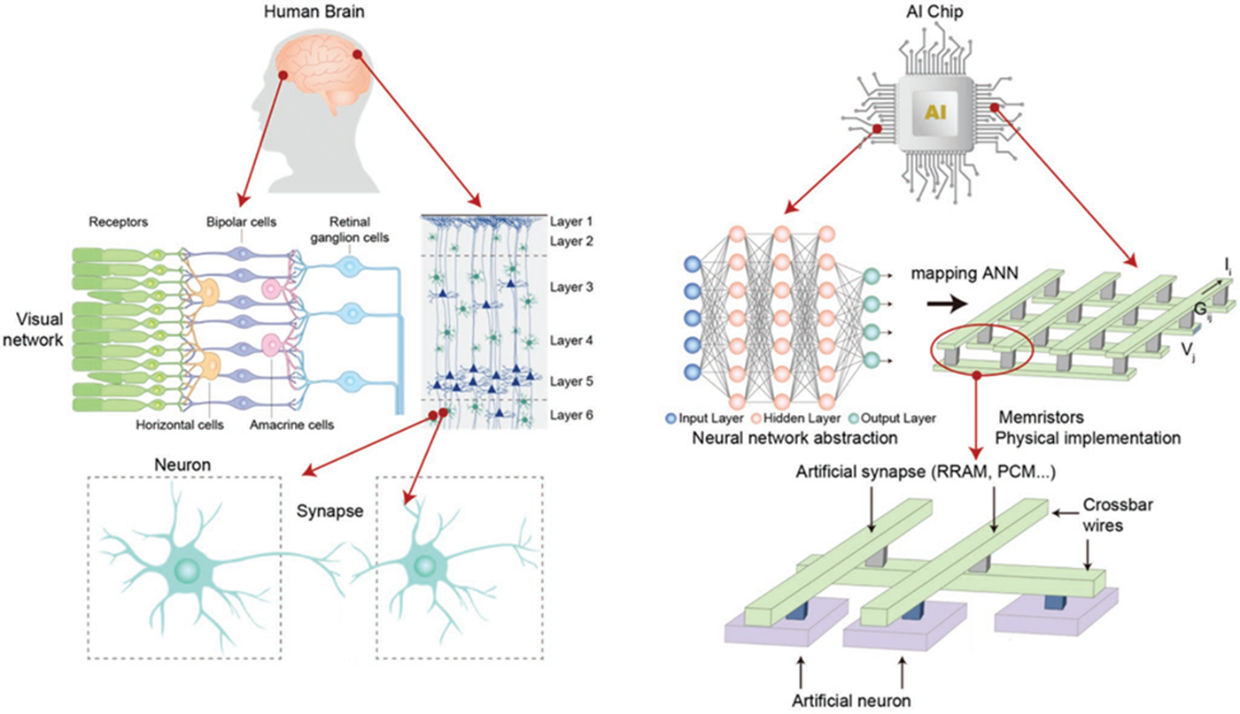
Figure 1. High-level comparison between the hierarchy of the human neural system and its implementation in an artificial neural network (ANN). The neural network graph shown on the right represents a software-level abstraction of the interconnectivity inherent to biological neural systems; for example, the visual network shown at the left. Recent advances directly implement this architecture within the hardware of ANN accelerators with crossbars serving as artificial neurons and the crossing points as artificial synapses. Adapted with permission from Reference 4. © 2019 Wiley.
Despite the occasionally staggering advances in deep learning, the tremendous energetic cost associated with developing, training, and ultimately inferring from the optimized network architecture is often swept under the rug. While some of the most advanced parallel computing platforms available offer performance measured in 1013 operations per second per watt,Reference Zhang, Lee, Liu, Shao, Keckler and Zhang11 the brain is estimated to operate orders of magnitude more efficiently, with approximately 1016 operations per second per watt.Reference Mead3 The stark contrast between comparable (oreven exceeding) levels of performance and profound disparity of energy expenditure highlight the distinction. While these systems may simulate neuromorphic functions, the restrictions imposed by the digital framework and the traditional von-Neumann architecture lead to immense power requirements that inhibit their use outside of server-based or enterprise-class computational facilities. Although various algorithmic proposals have been offered, no complete solution exists.Reference Han, Mao and Dally12
A growing realization that the next generation of neuromorphic computing must more effectively emulate, not just simulate, neural functions has led to a recent surge in research activity to discover, and in some cases revisit, materials systems that efficiently implement various neural functions.Reference Zhu, Zhang, Yang and Huang13 The underlying motivation is simple—by designing hardware that deeply emulates neural systems, we can achieve meaningful progress toward full neuromorphism.
In this vein, several technologies have emerged to support a transition from digital to analog computing to simulate the analog operation of the brain.Reference Tsai, Ambrogio, Narayanan, Shelby and Burr14 Most applications involving analog accelerators for deep learning make use of materials that can implement the primary neural functions of synaptic plasticity. Synaptic plasticity is the ability of synapses to strengthen or weaken in response to changes in activity. As synapses connect neurons, the strength of the synapse is equivalent to the weight of the connection. Plasticity can be short-term and long-term. Short-term plasticity is represented by rapid weight updates in a neural net, and long-term plasticity by the nonvolatility of the memory. Recent demonstrations of analog synapses using novel combinations of capacitors,Reference Kim, Gokmen, Lee and Haensch15 phase-change memory,Reference Ambrogio, Narayan, Tsai, Shelby, Boybat, di Nolfo, Sidler, Giordano, Bodini, Farinha, Killeen, Cheng, Jaoudi and Burr16 conductive bridge resistive random-access memory (RRAM),Reference Yao, Wu, Gao, Tang, Zhang, Zhang, Yang and Qian17 or electrochemical RRAMReference Fuller, Keene, Melianas, Wang, Agarwal, Li, Tuchman, James, Marinella, Yang, Salleo and Talin18 devices speak to some of the promising directions for future developmentReference Tang, Yuan, Shen, Wang, Rao, He, Sun, Li, Zhang, Li, Gao, Qian, Bi, Song, Yang and Wu4in neuromorphic computing.
Whereas neural networks allow for the simulation of neural functions, much work has also been focused on analog VLSI implementation of “silicon neurons” drawing directly from Carver Mead's vision of neuromorphism, whose ultimate goal is to directly emulate various neural functions within a fully analog VLSI system.Reference Indiveri, Linares-Barranco, Hamilton, van Schaik, Etienne-Cummings, Delbruck, Liu, Dudek, Häfliger, Renaud, Schemmel, Cauwenberghs, Arthur, Hynna, Folowosele, Saighi, Serrano-Gotarredona, Wijekoon, Wang and Boahen19,Reference Schuman, Potok, Patton, Birdwell, Dean, Rose and Planck20 Models have existed for years for generating an artificial neuron within VLSI systems that generate trains of voltage spikes.Reference Mahowald and Douglas21 A recent example however offers a complete analog system in which the artificial neuron's response to ionic currents is both fully modeled and implemented.Reference Abu-Hassan, Taylor, Morris, Donati, Bortolotto, Indiveri, Paton and Nogaret22 Nevertheless, despite significant progress in silicon neural emulation, a full implementation remains distant.
In an intriguing balance between simulation and emulation, organic electronics offers a unique opportunity. On one hand, the burgeoning field of organic bioelectronics offers the promise of a more natural communication between ionic biological signals and electronic device properties.Reference Simon, Gabrielsson, Tybrandt and Berggren23 On the other hand, utilization of the same material systems have led to dramatic advances toward artificial neural networks (ANNs) acceleration by way of an organic electrochemical RRAM architecture.Reference Fuller, Keene, Melianas, Wang, Agarwal, Li, Tuchman, James, Marinella, Yang, Salleo and Talin18Furthermore, the ability of conjugated polymers to undergo redox reactions with molecules present in the electrolyte lays out a hopeful future for various ways in which mixed ionic/electronic conducting systems could allow for a more naturally synthetic neuron by coupling chemical reactions to electronic signals.
Organic neuromorphic devices and systems: Abrief history
Many technologies and materials are currently being investigated for applications in hardware for neuromorphic computing. The invention of electronically switchable logic gates in 1999 heralded the heyday of molecular electronics.Reference Collier, Wong, Belhoradsky, Raymo, Stoddart, Kuekes, Williams and Heath24 In these two-electrode devices, a monolayer of organic rotaxane molecules was sandwiched between an aluminum electrode and a titanium electrode. The rotaxane acted as a nonvolatile switch between an “open” insulating state and a “closed” conducting state. The nonvolatile nature of this device made it immediately apparent that it could be used for architectures that take advantage of in-memory computing. Further research in the working mechanism of this device led to the development of the metal-oxide memristor,Reference Strukov, Snider, Stewart and Williams25 which has since become a workhorse of architectures for neuromorphic computing. These two-terminal devices can be set and reset in two distinct electronic states. Other devices giving rise to similar memristive behavior include oxide-based resistive devices, where oxygen defects give rise to filamentary conduction and nano-ionic metal filament forming devices. Finally, phase-change memories have been proposed as tunable resistors that emulate the fundamental nonvolatile and tunable nature of synapses.
Interestingly, while inorganic memristors can be traced back to a device containing an organic molecule, a rich literature of organic memristors developed in parallel exists.Reference Li, Qian, Zhu, Li, Zhang, Li, Ma, Li, Lu and Zhang26 In Figure 2, a schematic overview of organic-based conductive switching devices is presented. The ability to rationally design organic molecules, which allows tuning the switching voltage in addition to possibly accessing multiple redox states are some of the advantages of organic memristors. Endurance, reliability, and shelf life are their typical drawbacks. Recent results by Venkatesan et al. demonstrated organic memristive devices with excellent reproducibility, sub 50-ns switching, endurance of more than 1012 cycles, and stability greater than 106 s.Reference Goswami, Matula, Rath, Hedström, Saha, Annamalai, Sengupta, Patra, Ghosh, Jani, Sarkar, Mothapothula, Nijhuis, Martin, Goswami, Batista and Venkatesan27 Polymers have also been used in organic memristive devices, notably the poly(3.4-ethylenedioxythiophene) poly(styrene sulfonate) (PEDOT:PSS) blend. Forrest et al. reported a write-once-read-many-times (WORM) polymer-based two-terminal memory that takes advantage of a current-activated dedoping process to modulate the electrical properties of the active layer.Reference Möller, Perlov, Jackson, Taussig and Forrest28 Shaheen et al. used these devices as part of an organic “neuron” that performed simple pattern recognition.Reference Nawrocki, Voyles and Shaheen29

Figure 2. Organic electronic materials with conductance tuning and related mechanism. (a) Organic resistive switching based on conducting filaments or interface movements. (b) Redox-based switching with a counter redox reaction in a two-terminal configuration. (c)Redox-based switching in organic electrochemical transistors. (d) Conductance tuning based on nanoparticle charge-trapping.Reference van de Burgt, Melianas, Keene, Malliaras and Salleo47
A different family of devices includes a third-gate terminal. As described in the van de Burgt and GkoupidenisReference van de Burgt and Gkoupidenis30 article in this issue, organic electrochemical devices with three terminals add a degree of freedom and allow for a different variety of applications. Three-terminal neuromorphic devices present advantages and added challenges compared to their two-terminal counterparts. On one hand, the third terminal confers an added degree of control to the electronic state of the device channel allowing decoupling of the write and read operations as those signals do not flow through the same terminals. Such decoupling is the key to the low-energy operation of three-terminal devices as it allows both write and read processes to be performed at low voltages without any interference. On the other hand, the third terminal complicates wiring and poses problems in terms of integration and scaling as the device and the wiring occupy more area than a two terminal device, which is easily amenable to integration in an array of crossing electrodes (crossbar array) for instance.
The first organic three-terminal devices displaying some neuromorphic electrical characteristics were designed to take advantage of the kinetics of charge trapping in metal nanoparticles scattered in the device channel.Reference Novembre, Guérin, Lmimouni, Gamrat and Vuillaume31 These devices were operated as field-effect transistors or as electrolyte-gated transistorsReference Desbief, di Lauro, Casalini, Guérin, Tortorella, Barbalinardo, Kyndiah, Murgia, Cramer, Biscarini and Vuillaume32 and displayed potentiation and depression effects, which could be modulated by the gate pulsing frequency.Reference Alibart, Pleutin, Guérin, Novembre, Lenfant, Lmimouni, Gamrat and Vuillaume33 This behavior does in fact bear an analogy to that of biological synapses.
The use of an electrolyte brings another analogy with biological synapses that has not been achieved with inorganic neuromorphic devices. In the majority of biological synapses, the signal transmitted across the synapse is not electrical but chemical, carried by neurotransmitters that act on the receptors, which then alter the state of the postsynaptic neuron in an interplay with ions present in the surrounding medium. It is thus attractive to use both ionic and electronic fluxes in artificial synapses; in doing so, it may be easier to replicate some of the important functions of the biological synapses in neuromorphic computing operations. There is an entire family of organic semiconductors that is capable of conducting ions and electrons.Reference Paulsen, Tybrand, Stavrinidou and Rivnay34 In recent years, these materials have indeed been exploited to make organic neuromorphic devices. Other materials, such as hybrid organic–inorganic perovskites also display significant ionic transport and as a result, have also been the object of attention for neuromorphic devices.
In the first example of an electrochemical transistor used as a memristor, Erokhin et al. fabricated a device with a polyaniline channel, a polyethyleneoxide:LiCl electrolyte, and a silver wire as a gate electrode.Reference Erokhin, Berzina and Fontana35 While the measured drain current did not display the desired hysteretic behavior, which would impart memristive properties to the device, the gate current did, and as a result the differential current (i.e., drain current minus gate current) did as well. These characteristics were recognized as being caused by the kinetics of ion drift and were hypothesized as the basis for the use of these devices in networks that would display learning. The synapse-like properties of these devices were further improvedReference Berzina, Smerieri, Bernabò, Pucci, Ruggeri, Erokhin and Fontana36 leading to the demonstration of a two-layer network capable of XOR logic classification.Reference Emelyanov, Lapkin, Demin, Erokhin, Battistoni, Baldi, Dimonte, Korovin, Iannotta, Kashkarov and Kovalchuk37 The same device architecture was used in a more biomimicking function to simulate the synaptic dysfunction associated with Alzheimer's disease.Reference Battistoni, Erokhin and Iannotta38
More recently, the same group coupled cortical neurons in brain slices with these organic artificial synapses and showed communication between the neurons mediated by an organic-based synapse.Reference Juzekaeva, Nasretdinov, Battistoni, Berzina, Iannotta, Khazipov, Erokhin and Mukhtarov39 The range of demonstrations where organic electrochemical devices are used in a neuromorphic function is a testament to their versatility and potential in brain–machine interfaces. The biomimicking aspect of polymer-based electrochemical devices was further explored by Lee et al., who fabricated a core-sheath structure reminiscent of a neuron axon.Reference Xu, Min, Hwang and Lee40 The structure was formed by spraying a solution of a polythiophene-based semiconductor and an electronically insulating, but ionically conducting polymer, through a metal nozzle. The authors found that the materials self-assembled with a semiconducting core and an insulating sheath. This structure was successively covered in a gel electrolyte and connected electrically to complete the device. A voltage imposed with an electrode in the gel caused an excitatory postsynaptic current that modulated the state of the device. Thanks to miniaturization of the device channel down to ~300 nm, potentiation, depression and spike time-dependent plasticity were demonstrated with energy consumption per synaptic event lower than 10 fJ, an important milestone as this figure rivals that usually associated with biological synaptic events. The use of electrochemical transistors to perform typical neuromorphic operations was further developed by Gkoupidenis et al., who showed potentiation and adaptation in single devices.Reference Gkoupidenis, Schaefer, Garlan and Malliaras41 Device arrays were used to simulate higher functions such as orientation selectivity, homeoplasticity, and functional connectivity by global voltage oscillations (as described in the van de Burgt and GkoupidenisReference van de Burgt and Gkoupidenis30 article in this issue).Reference Gkoupidenis, Koutsouras, Lonjaret, Fairfield and Malliaras42–Reference Koutsouras, Prodromakis, Malliaras, Blom and Gkoupidenis44
In another approach, the article by Perez and Shaheen in this issue90 presents a design strategy for using electrochemical transistors in neuromorphic circuits aimed at demonstrating Boolean and reversible logic. It utilizes neuronal circuit structures similar to those of Emelyanov et al.,37 but based solely on three-terminal electrochemical devices without the need for memristors or CMOS transistors. They demonstrate XOR logic classification that can then be scaled to larger circuits based on Boolean or reversible logic, while taking advantage of the pathways to ultralow energy consumption afforded by the underlying neuromorphic structure.
The architecture of conventional electrochemical transistors makes it challenging for these devices to exhibit nonvolatility. The use of redox-active molecules in the electrolyte was shown to mitigate this problem to some extent, with these organic memories displaying retention of a few seconds.Reference Das, Pillai, Wu and McCreery45 In a different approach, van de Burgt et al. increased the capacitance of the gate electrode while maintaining its polarizability.Reference van de Burgt, Lubberman, Fuller, Keene, Faria, Agarwal, Marinella, Talin and Salleo46 This new device architecture enabled the demonstration of hundreds of analog conductance states, linear tuneability, low write noise and sub-μs write–read cycles, while exhibiting state retention on the order of hours. These devices were used to demonstrate the parallel update of nine devices in a small 3 × 3 array.Reference Yao, Wu, Gao, Tang, Zhang, Zhang, Yang and Qian17
From the device perspective, there has been steady progress in the architecture and the choice of organic materials optimized for neuromorphic functions.Reference van de Burgt, Melianas, Keene, Malliaras and Salleo47 Importantly, the material requirements may be different than for traditional thin-film devices such as diodes or transistors. For instance, for scalability, organic memories should exhibit high resistance, and as a result, low-carrier mobilities are desirable. Furthermore, semiconductor capacitance and ability to intercalate ions is of paramount importance, a property not relevant to conventional electronic devices. As a result, this new promising application of organic semiconductors opens up new design spaces for organic semiconductors.
Opportunities and challenges: The road ahead
Looking ahead, we believe that significant opportunities and also challenges lie ahead for the field of organic neuromorphic devices along three important frontiers: integration with biology, manufacturing/customization of large area and three-dimensional (3D) forms, and the application in novel computing architectures. Finally, we discuss challenges and opportunities in hybrid organic–inorganic halide perovskites for neuromorphics (a topic covered by Harikesh and co-authors in this issueReference Harikesh, Febriansyah, John and Mathews48).
Integration with biology
An obvious application for all neuromorphic devices is in biomedical applications. Biocompatibility, inherent sensitivity, and soft mechanical properties make organic neuromorphic devices particularly suitable for integration with biology. This is a front that is receiving a great deal of attention. Juzekaeva et al. recently provided a powerful demonstration wherein an organic memristive device was used to connect two live neurons.Reference Battistoni, Erokhin and Iannotta38 The device, based on polyaniline and a lithium salt-doped polyethylene oxide, acted as an artificial synapse, enabling the unidirectional and activity-dependent coupling of the neurons. The spike-timing features of the device were engineered to be similar to those of natural excitatory synapses, therefore, the synaptic strength was regulated by neuronal activity, allowing neuronal synchronization. In a similar vein, the connection of live neurons to silicon neurons was demonstrated by Serb et al.,Reference Serb, Corna, George, Khiat, Rocchi, Reato, Maschietto, Mayr, Indiveri, Vassanelli and Prodromakis49 using inorganic memristors.Reference Novembre, Guérin, Lmimouni, Gamrat and Vuillaume31,Reference Gupta, Serb, Khiat, Zeitler, Vassanelli and Prodromakis50 Recently, it was demonstrated that biological cells can directly modulate the long-term state of organic neuromorphic devices depending on the amount of neurotransmitter released.Reference Keene, Lubrano, Kazemzadeh, Melianas, Tuchman, Polino, Cinà, van de Burgt, Salleo and Santoro51 This work shows how integrated adaptive connections can work for hybrid biological/neuromorphic systems.
Artificial sensory neurons capable of learning and signal processing were demonstrated by Wan et al.Reference Wan, Chen, Fu, Wang, Matsuhisa, Pan, Pan, Yang, Wan, Zhu and Chen52 and by Yoon et al.Reference Yoon, Wang, Kim, Wu, Ravichandran, Xia, Hwang and Yang53 using inorganic memristors. Kim et al. took this a step further by developing a bioinspired artificial afferent nerve (inbiology, afferent nerves receive signals from sensory organs and transmit them to the central nervous system) based on a three-terminal organic neuromorphic device.Reference Kim, Chortos, Xu, Liu, Oh, Son, Kang, Foudeh, Zhu, Lee, Niu, Liu, Pfattner, Bao and Lee54 The device used a conjugated polymer and an ion gel receiving input from a ring oscillator connected to a pressure sensor, all on a flexible substrate (Figure 3). This combination enabled the sensing of pressure, the conversion of the signal to action potential-like spike trains, and their subsequent processing by the neuromorphic device. The output of the device drove the twitching motion of a cockroach leg, providing a demonstration of a hybrid bioelectronic reflex.
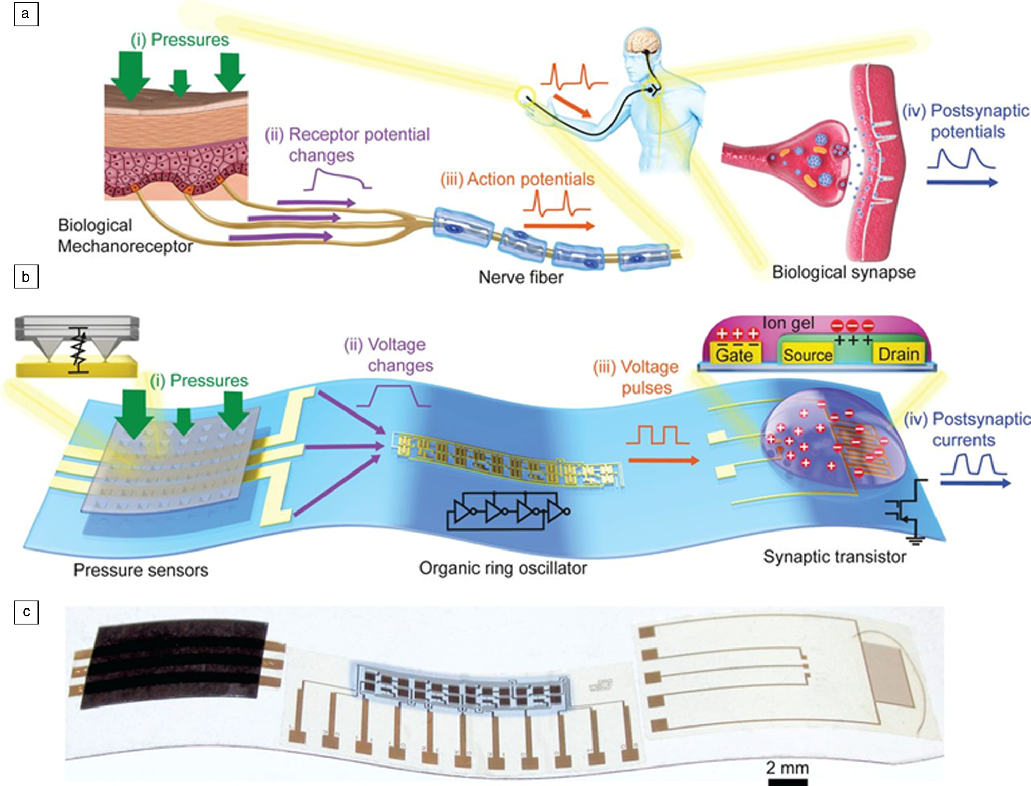
Figure 3. (a) Schematic of the afferent nerve, where applied pressure initiates action potentials. (b) Concept of the artificial afferent nerve comprising pressure sensors, a ring oscillator, and a three-terminal neuromorphic device (synaptic transistor). (c) Photograph of an artificial afferent nerve. Reprinted with permission from Reference 54. © 2018 AAAS.
These examples pave the way for adaptive systems, where the coupling between organic active layers and biology allows for a direct feedback and control of the material by the host environment and vice versa.Reference van Dormaele, Gkoupidenis and van de Burgt55 Smart neuromorphic biosensors that not only sense, but also control, and act upon different inputs from the environment in an optimized and personalized manner will soon become available. These can lead to all hardware-based, closed-loop, smart drug delivery systems in, for instance, glucose sensing and insulin delivery, or seizure detection and release of antiepileptic drugs. Another opportunity is in smart neuroprosthetics, where the interface between the human nerve and prosthetic system can be trained by and learn from the biological signals surrounding them, leading to an optimized connection between the prosthetic and host. Osborn et al. demonstrated a neuromorphic prosthesis in which artificial skin perceives touch and pain;Reference Osbron, Dragomir, Betthauser, Hunt, Nguyen, Khaliki and Thakor56in silico neurons process the signal and provide tactile information to an amputee. It is only a matter of time before the in silico neurons are replaced by neuromorphic devices, dramatically reducing device complexity and energy consumption, and increasing portability.
Neuromorphic circuits based on organic materials are promising platforms for inference in biosensing. Sensing properties can be integrated with device operation. This means that training sets and inference processes can readily be biosensing primitives, thus merging signal acquisition and feature extraction. Right now, the worlds of acquisition and processing are still distinguishable,Reference Kim, Chortos, Xu, Liu, Oh, Son, Kang, Foudeh, Zhu, Lee, Niu, Liu, Pfattner, Bao and Lee54,Reference Lee, Seo, Lee, Lee, Lee, Cheon, Cho, Lee, Chung, Park, Kim and Hong57 especially in bioelectronics. Another opportunity is in the area of point-of-care diagnostics. Generic diagnostic systems are envisioned, with functions defined by the end-user through training.Reference Kim, Chortos, Xu, Liu, Oh, Son, Kang, Foudeh, Zhu, Lee, Niu, Liu, Pfattner, Bao and Lee54 This approach has the potential to increase throughput in manufacturing, adopting the approach of “one platform for many applications” in analogy with classic microcontrollers/FPGAs (field-programmable gate arrays).
Finally, integration with biology can also inform the development of more sophisticated neuromorphic devices. The dynamic response of biological neurons is influenced by a multitude of ionic and other biochemical signals, as described in this issue in the article by van de Burgt and Gkoupidenis.Reference van de Burgt and Gkoupidenis30 This paradigm endows biological neural networks with inherent parallelism and information processing efficiency. This can serve as a model for the development of organic neuromorphic devices that are capable of receiving multiple inputs from biological systems. Future communication between neuromorphic circuits and living systems will rely on more mechanisms than just capacitive coupling mediated by ions.
Challenges of scaling up and customization
Different applications of neuromorphic devices will require different levels of integration. For example, high-performance computing architectures require, in general, high levels of integration, little device-to-device variability, high device reliability, and possibly compatibility with high fabrication temperatures for integration with conventional CMOS electronics. On the other hand, there are a number of applications that would benefit from large area devices with a medium to low level of integration, or even 3D device structures offering better integration with their environment. These include systems for environmental intelligence and pattern recognition in large areas/complex shapes (noise, moisture, mechanical deformations, temperature, chemical and radiation profiling/mapping in areas such as environmental sensing, agriculture, and structure integrity). Such systems can also serve as a rough collection of training sets for more advanced/finer in silico classification. Similarly, large areas and 3D forms would also be useful in the field of bioelectronics, where spatially distributed processing, classification, and actuation units can potentially interact over space and time with the body or whole organs.
Photolithography has until now been the key fabrication technique used when fabricating organic neuromorphic devices, such as those discussed so far in this article. This is partly because the approach readily integrates with existing electronic device and microfluidics fabrication processes, but is often due to the existing confidence in and familiarity with the process technology. Photolithography is often the ideal choice for in-depth scientific research because of its high resolution, ability to deliver high yields, and availability in research labs. However, alternative routes to manufacturing should be examined to address large-area, mass customization, and 3D forms, where the use of lithography is challenging. Moreover, there are significant trends observable in industry where low-volume, niche, or late-stage customized manufacturing is driving a shift away from standard high-throughput manufacturing techniques. This is especially true for healthcare technologies, with a shift toward remote monitoring, home testing, and more personalized treatments.58 Organic neuromorphics are anticipated to be beneficial in creating low-energy sensors, and these same trends toward digitally enabled manufacturing of devices have also been noted in printed electronics for use in smart, sustainable building envelopes and consumer products, and functionalizing construction materials such as glass, cement, or ceramic tiles.Reference Orozco-Messana, Daly and Zanchetta-Chittkaa59
With this motivation to scale up product customization, a wide range of techniques are available for late-stage, digitally enabled functional material patterning, with inkjet printing, 3D printing by fused deposition modeling (FDM), and laser deposition being the most commonly explored. There have been many reported printed devices, such as transistorsReference Chung, Cho and Lee60 and photovoltaicsReference Jung, Sou, Banger, Ko, Chow, McNeill and Sirringhaus61 with inkjet printing and printed sensors with FDM.Reference Ota, Emaminejad, Gao, Zhao, Wu, Challe, Chen, Fahad, Jha, Kiriya, Gao, Shiraki, Morioka, Ferguson, Healy, Davis and Javey62 With the ease of formulation of organic semiconductors into functional fluids and gels along with their sensitivity to laser-based processes, additive manufacturing (AM) by inkjet printing and FDM will be the key approaches for customized device development and the future of organic neuromorphics.
As devices shift toward digital fabrication, the final integrated device behavior is very dependent on the processing steps, and manufacturing-related research challenges must be tackled while still at a low “technology readiness.” The field of organic neuromorphics can learn at this early stage from both standard digital fabrication industry challengesReference Hoath63 and also challenges faced by other fields that have recently shifted to AM patterning, such as in the field of pharmaceutics.Reference Daly, Harrington, Martin and Hutchings64Figure4a summarizes the journey of functional materials when fabricating a device by AM, and specifically with inkjet printing or FDM (Figure 4b), with each step incorporating its own challenges noted briefly here.

Figure 4. (a) During additive manufacturing, organic materials will undergo multiple steps, where studies will be needed to determine the effect on final functionality.Reference Daly, Harrington, Martin and Hutchings64 (b)Inkjet printing (left) and fused deposition modeling (right).Reference Willis-Fox, Rognin, Aljohani and Daly67 Images courtesy of E. Rognin, University of Cambridge. (c) Digital photo of a 3D printed transistor channel, with the overall device 35mm in length. Image courtesy of T. Mangoma, University of Cambridge.
First, there must be a focus on reformulation to meet the requirements for digital fabrication. Scaling up while ensuring no reduction in functionality and stability under storage is a major challenge for advanced functional materials.Reference Paton, Varrla, Backes, Smith, Khan, O'Neill, Boland, Lotya, Istrate, King, Higgins, Barwich, May, Puczkarski, Ahmed, Moebius, Pettersson, Long, Coelho, O'Brien, McGuire, Mendoza Sanchez, Duesberg, McEvoy, Pennycook, Downing, Crossley, Nicolosi and Coleman65 When printing functional macromolecules, it is important to understand the forces they experience as they flow through pipes, pumps, and ancillary equipment, and that the shear, extensional, or thermal forces are not having a deleterious effect,Reference Rognin, Willis-Fox, Aljohani and Daly66 as is also the case for flow through printheads and nozzles.Reference Willis-Fox, Rognin, Aljohani and Daly67,Reference Willis-Fox, Rognin, Baumann, Aljohani, Göstl and Daly68 Once out of the nozzle, there are complex interdependencies between the formulation and printing actuation that determine if stable, repeatable drop or filament formation is feasible. This is often a key point that then requires additional formulation modification with the addition of viscosity and surface tension modifiers. Stable line formation is especially challenging in inkjet printing, with a complex balance between the interfacial energies and substrate properties,Reference Hsiao, Martin and Hutchings69 but again critical if trying to ensure stable interconnects between printed components. The drying or curing during inkjet printing and the layer solidification for FDM then determine the final successful transfer of function to a surface; however, to ensure scalability, it is critical to also consider the lifetime of the device, the surface adhesion and ability to withstand the forces present in the device use. These are often neglected challenges until high “technology readiness” is achieved but require significant analysis, reformulation, or process technology modification to solve. As indicated in Figure 4, these challenges need to be considered as the layers build up because of the different underlying surface or thermal dissipation that will be present. However, if these are considered and taken care of, neuromorphics can be scaled up to many 100s of layers to create affordable and complex devices.
By reviewing the known challenges for fluid-based AM techniques, it is also clear that fused deposition modeling may in fact provide an important route forward. This AM technique has a history of rapid functional filament development, well-characterized nozzle flow behavior, requires almost no surface preparation, has a long history of easily controlled printability, and is clearly suitable for structures of many hundreds of layers in thickness. A simplified printed transistor channel is shown in Figure 4c. The black electrodes at the edge are covered with a white flexible insulator, all made by FDM. An inkjet printed organic semiconductor in the middle is covered by a liquid gate, ready for testing. The major challenge of integration into future devices is going to be in design, where complex 3D printed, multimaterial structures do not lend themselves to sharing an electrolyte. Again, the move to manufacturing may require examination of another field, for example, learning from the field of tissue engineering. A similar challenge of sharing and accessing a common functional fluid has led to scaffold designs by FDM with complex vascularization.Reference Guy, Justin, Aguilar-Garza and Markaki70
Novel computing architectures
A major opportunity for organic neuromorphic devices is in novel computing architectures that offer low-power consumption. Many neuromorphic applications are most useful at “the edge,” which means that there is a clear benefit to train and use these systems locally and not require a connection to the cloud. One obvious example is driverless autonomous cars that have to operate safely even in remote areas where internet connectivity is scarce. The low-power use of organic neuromorphic materials offers this functionality.Reference van de Burgt, Lubberman, Fuller, Keene, Faria, Agarwal, Marinella, Talin and Salleo46,Reference Ling, Koutsouras, Kazemzadeh, van de Burgt, Yang and Gkoupidenis71,Reference Pecqueur, Vuillaume and Alibart72 Another class of devices where low-power use is critical are battery operated devices such as lab-on-a-chip and point-of-care devices that require some form of training and ability to continue to learn and adapt, without the possibility of cloud connectivity.
Reservoir computing presents untapped opportunities to apply organic semiconductors to hard computational problems. Recent work has shown that reservoir computing can be used for model-free estimation of Lyapunov exponents in prototypical chaotic dynamical systems such as the Lorenz system.Reference Pathak, Lu, Hunt, Girvan and Ott73 The result can then be used to predict the short-term behavior of the system with surprising precision or to simulate long-term behavior while closely replicating its ergodic properties for arbitrary time into the future. This is possible since the reservoir presents a high-dimensional space from which a subset of dynamical components is chosen, through training of the output weights that effectively capture the underlying structure of the original system. Recent follow-up work has shown that the technique can be improved by dynamical noise,Reference Banerjee, Pathak, Roy, Restrepo and Ott74 a counterintuitive but potentially useful result from the standpoint of physical implementation in neuromorphic computing. The implication for organic semiconductor-based approaches is that variations in neuronal response due to imperfect fabrication, or noise and fluctuations in the electronic response of individual neurons, may be harnessed as beneficial properties in the correct regimes of operation.
As our understanding and control of mixed-mode, switchable behavior in organic semiconductors increases, so does the application space of computing paradigms. Many approaches to unconventional computing can be envisioned.Reference Adamatzky75 For example, cellular automata (CA) computing with discrete organic semiconductor devices can be envisioned, in which the state of each cell in a matrix evolves with time according to simple rules based on the prior state of that cell and its neighbors. At smaller spatial scales, the dynamics of nanoscale and molecular materials could themselves be harnessed for computation via in materio computing, in which a material is used directly as the substrate for the computation; “One is instead computing ‘close to the physics,’ doing what comes naturally, and therefore (hopefully) efficiently.”Reference Stepney76 Many of the exotic ideas found in the arena of unconventional computing have been circulating for many decades, dating back to von Neumann and Turing. Now may be the time to revisit many of them in the context of organic semiconductor materials given how far the field has advanced in recent years.
Hybrid organic–inorganic halide perovskites
Organic–inorganic halide perovskites (HPs) have been extensively re-explored in the last decade and have shown exciting results in photovoltaics and light-emitting diodes. As the hybrid moniker would suggest, these materials combine the properties and advantages of organic semiconductors with those of their inorganic counterparts. These ionic semiconductors are processable via solution processing/vacuum techniques while the organic cation in the hybrid structure enables structural and electronic tunability. Unique to halide perovskites, is the coexistence and coupling of ionic and electronic components of current allowing for a myriad of mechanisms to be exploited.Reference Tress80 In terms of electrically driven neuromorphic elements, the mechanisms noted are ones that are used to explain switching in inorganic counterparts (ionic migration, electrochemical metallization) as well in organic semiconductors (ionic doping).Reference Choi, Han, Hong, Kim and Jang81 Artificial synapses utilizing vacancy-driven halogen migration and electrochemical metallization reactions are the most widely adopted to date.Reference Xiao and Huang82–Reference Tian, Zhao, Wang, Yeh, Yao, Rand and Ren84 The ability to regulate redox reactions controlling the flux of ionic species makes this approach widely applicable to all deep learning inference engines that require a medium-to-high degree of computational precision. Exploitation of the intrinsic ionic-electronic charge transport in halide perovskites, that is, modulating the distribution of ions within the perovskite layer to self-dope and regulate carrier injection barriers at the perovskite-charge injection layer seems to be the most promising alternative.Reference John, Yantara, Ng, Narasimman, Mosconi, Meggiolaro, Kulkarni, Gopalakrishnan, Nguyen, Angelis, Mhaisalkar, Basu and Mathews85 Since the flux of ionic species can also in turn be externally modulated via spike-based input patterns, realization of unsupervised learning in spiking neural networks utilizing local learning rules such as spike-timing dependent plasticity (STDP) is also feasible. By exploiting the excellent optoelectronic properties of HPs, new memristors that can be programmed via both electrical and optical programming spikes have been recently realized.Reference Zhu, Lee and Lu86,Reference Pradhan, Das, Li, Chowdhury, Cherusseri, Pandey, Dev, Krishnaprasad, Barrios, Towers, Gesquiere, Tetard, Roy and Thomas87 This paves the way for new optoelectronic neuromorphic architectures that combine multiple modalities for accessing memory states.
Many of the challenges facing halide perovskite memristors are ones common to any new material entrant, while the more established oxide materials face some challenges as well.Reference Burr, Shelby, Sebastian, Kim, Kim, Sidler, Virwani, Ishii, Narayanan, Fumarola, Sanches, Boybat, Gallo, Moon, Woo, Hwang and Leblebici88 From a device physics perspective, achieving multiple programmable conductance states in a true analog fashion across a wide dynamic conductance range with low write noise is very challenging. Other challenges include limited retention of distinct memory states, endurance of the switching characteristics and number of programmable conductance states. From a system perspective, managing device-to-device variations and scaling up to large arrays are other major concerns that need to be addressed. Practical implementation of synaptic arrays would finally require integration with CMOS digital circuits (e.g., selectors and driver transistors) at some level. This integration is yet another challenge that needs to be solved.
From a materials point of view, the usage of Pb and toxic solvents will have to be reduced. Initial indications point to this being an easier substitution for memristors than for other areas such as photovoltaics. Indicative of the nascent nature of this area, most current HP-based memristive implementations are limited to dot-point structures with analyses focused on conventional digital logic parameters such as ON-OFF ratio. Crossbar implementations and systematic analysis of the analog programming window are lacking and hence, do not sufficiently address the scaling and algorithm aspects pertaining to large-scale artificial neural networks (ANNs). Metallization reactions exploited by most HP-based memristors result in irreversible metal-HP electrochemical reactions, often limiting the device reliability, endurance, and memory retention. In addition, most devices require a forming process to induce stable switching behavior that results in unnecessary power- and time-consuming steps to program nonvolatile states during training and online inferencing. While elemental demonstrations of optoelectronic HP memristors have been demonstrated, developing algorithms that can cater to the physics of optoelectronic switching and realizing optical interconnects to address these elements via light pulses at a system level still remain major challenges.
The versatility of halide perovskites allow for multiple avenues for exploration.Reference Sum and Mathews89 Halide perovskites are processable through a wide variety of techniques, including large-area printing and thermal evaporation allowing them to be considered for printed neuromorphic sensor applications as well as for heterogeneous integration with Si-CMOS technology. Moreover, the compositional space possible in halide perovskites is high and the inclusion of layered perovskites, double perovskites, and other vacancy modulated halide structures further boosts this versatility (>106 compositions). Significantly, much of this compositional space can be traversed through solution-based means by an appropriate choice of the starting precursors and mild processing. Due to the complex interplay of templating organic ions, and the heavy metal halide lattice, halide perovskites that display chiral optical properties, piezoelectricity, spin-dependent charge transport, ferroelectricity, and even multiferroic behavior are possible. Such a myriad of properties has not yet been explored in the fabrication of synapses and other neuromorphic elements. This would allow halide perovskites to be examined for architectures beyond electrical control.
Conclusion
The field of brain-inspired computing is enjoying rapid expansion at the moment, with intense interest across scales from materials to devices to circuits and across the development pipeline from fundamental science to industrial prototypes. A side effect of this intense interest is that nearly any type of switching behavior can be considered as the basis for a brain-inspired approach, which might for instance exhibit neuronal behavior such as short- and long-term potentiation and spike-timing-dependent plasticity. One can attend many conference talks that end in a statement about the promise of a given material for brain-inspired computing simply founded on an unexpected (and perhaps unexplained) switching behavior. While such mass excitement about new ideas provides an important propelling force for the field, it also creates many dead-end pathways in which there may be no practical way to implement a given switching behavior into a computing system at industrial scale and in a competitive way. However, to quote C. Rigetti, “pumping entropy out of the vision”77 is required to reduce the number of potential developmental pathways toward practical, scalable brain-inspired computers. A technique we have for this is co-design, in which the design and implementation of materials, devices, systems, and applications are conceived of and worked on simultaneously.Reference Planck, Rose, Dean, Schuman and Cady78,79 In this way, roadblocks that might have arisen are ideally foreseen at the onset of the design process. This is important since with any complex material substrate, the information processing behavior at the systems level is inexorably linked to the physical behavior at the nanoscale molecular level.
Viewed from another angle, the link between structure and performance raises the issue of lack of universality in organic neuromorphics. There are many promising materials approaches but still not a single/few champion material(s). This is problematic because scientific effort is spread thin among different materials and device architectures. As the field advances in the future, winners are expected to emerge, which will help concentrate the effort and yield a deeper understanding of mechanisms and structure versus neuromorphic properties relationships. This will also help in understanding parasitic effects arising from for instance, reactions of ions at interfaces, which are comparatively present more in small devices, leading to improved retention of the conductance states and more stable materials and devices in general.
Finally, it is important to note that there is still a debate in neuroscience about which are (and to which degree) the computational primitives of biological neural networks that contribute to intelligence (plasticity, spike coding, and global phenomena). Our community should keep a close eye on this debate, as future advances in materials science should go hand in hand with advances in neuroscience in order to unravel the full potential of organic materials for neuromorphic computing.
Acknowledgments
T.N.M., R.D., and G.G.M. acknowledge funding by the EPSRC and Centre for Doctoral Training in Ultra Precision Engineering. Y.v.d.B. acknowledges funding from the European Union's Horizon 2020 Research and Innovation Programme, Grant Agreement No. 802615. A.S. and Y.T. acknowledge funding from the National Science Foundation and the SRC, E2CDA Program Award No. 1739795. R.A.J. and N.M. would like to acknowledge the funding from MOE Tier 2 Grant No. MOE2018-T2-2-083. S.E.S. acknowledges funding from the University of Colorado Boulder Research Innovation Office Seed Grant Program.
 Yaakov Tuchmanis a doctoral candidate in the Department of Materials Science at Stanford University. He received his BA degree in physics from Yeshiva University in 2014. His research includes organic mixed ionic/electronic conductive materials. His current research focuses on integrating organic semiconductors with traditional nanofabrication processes to build and characterize the next generation of organic electrochemical resistive memory devices. Tuchman can be reached by email at ytuchman@stanford.edu.
 Tanyaradzwa N. Mangomais a doctoral candidate in the Department of Engineering at the University of Cambridge, UK. She obtained her integrated Masters of Engineering degree in materials science and engineering from the University of Manchester, UK, in 2017. She undertook a placement year at Xaar plc, UK, and completed her dissertation at the Henry Royce Institute, UK, and the Diamond Light Source, UK. She then joined the Ultra-precision Engineering Centre for Doctoral Training where she has worked with the Nanomanufacturing, Fluids in Advanced Manufacturing and Bioelectronics groups at the University of Cambridge. Her current research focuses on additive manufacturing of organic neuromorphic devices and neural networks. Mangoma can be reached by email at tm617@cam.ac.uk.
 Paschalis Gkoupidenishas been a group leader in the Department of Molecular Electronics at the Max Planck Institute for Polymer Research, Germany, since 2017. He earned his PhD degree in materials science from the National Centre of Scientific Research “Demokritos” Greece, in 2014. His doctoral research focused on ionic transport mechanisms of organic electrolytes, and physics of ionic-based devices and of nonvolatile memories. He conducted postdoctoral research in 2015 in the Department of Bioelectronics at École des Mines de Saint-Étienne, France, focusing on the design and development of organic neuromorphic devices based on electrochemical concepts. Gkoupidenis can be reached by email at gkoupidenis@mpip-mainz.mpg.de.
 Yoeri van de Burgthas led the Neuromorphic Engineering Group at Eindhoven University of Technology, since 2016, and has been a visiting professor at the University of Cambridge, UK, in 2017. He obtained his PhD degree at Eindhoven University of Technology, The Netherlands, in 2014. He briefly worked at a high-tech startup in Switzerland, after which he obtained a postdoctoral fellowship in the Department of Materials Science and Engineering at Stanford University. He was recently awarded an ERC Starting Grant from the European Commission. In 2019, he was elected as a Massachusetts Institute of Technology innovator Under 35 Europe. His research focuses on organic neuromorphic materials and electrochemical transistors. Van de Burgt can be reached by email at Y.B.v.d.Burgt@tue.nl.
 Rohit Abraham Johnis a research fellow at Nanyang Technological University (NTU), Singapore. He received his PhD degree from NTU in 2019. His research focuses on neuromorphic electronic devices, oxide semiconductors, thin-film transistors, and memory devices. John can be reached by email at rohitabrahamjohn@ntu.edu.sg.
 Nripan Mathewsis an associate professor and Provost's Chair in Materials Science and Engineering in the School of Materials Science and Engineering at Nanyang Technological University (NTU), Singapore. He obtained his bachelor's degree in materials engineering from NTU and his MSc degree under the Singapore-Massachusetts Institute of Technology Alliance. After obtaining his PhD degree from Paris VI University, France, he was a visiting scientist at École Polytechnique Fédérale de Lausanne, Switzerland. His research interests focus on the development of novel and inexpensive electronic materials through cost-effective techniques for electronics and energy conversion. These include organic−inorganic halide perovskites, metal oxides, and organic thin films. Mathews can be reached by email at Nripan@ntu.edu.sg.
 Sean E. Shaheenis an associate professor of electrical, computer, and energy engineering and associate professor by courtesy of physics at the University of Colorado Boulder. He obtained his BS degree in physics from Carnegie Mellon University in 1991, and his PhD degree in physics from The University of Arizona in 1999. He was a staff scientist at the National Renewable Energy Laboratory from 2002 to 2007, and then a faculty member in the Department of Physics and Astronomy at the University of Denver from 2007 to 2013. His research focuses on emerging photovoltaic, photonic, and neuromorphic materials and devices. He is currently the editor-in-chief for the SPIE Journal of Photonics for Energy and director of the NSF RET program site on Authentic Research Experiences for Teachers (ARETe): Connecting Community College Faculty and Students to University Engineering and Computer Science Labs at the University of Colorado Boulder. Shaheen can be reached by email at sean.shaheen@colorado.edu.
 Ronan Dalyis a senior lecturer at the Institute for Manufacturing in the Department of Engineering at the University of Cambridge, UK, where he leads the Fluids in Advanced Manufacturing Research Group and Inkjet Research Centre. He completed his first degree in chemical engineering at The University of Edinburgh, Scotland. He was a process technology manager at Unilever. He completed his PhD degree in chemistry at Trinity College Dublin, Ireland. His research interests focus on chemical and physical phenomena of polymeric, biological and nanomaterials when exposed to laser processing and advanced fluid-based processing, such as extrusion and additive manufacturing. Daly can be reached by email at rd439@cam.ac.uk.
 George Malliarasis the Prince Philip Professor of Technology at the University of Cambridge, UK. He received his PhD degree from the University of Groningen, The Netherlands. He was a faculty member at Cornell University and École des Mines, France. He received awards from the New York Academy of Sciences, the National Science Foundation, and DuPont. Malliaras received an honorary doctorate from the University of Linköping, Sweden. He is a Fellow of the Materials Research Society and the Royal Society of Chemistry, and he serves as deputy editor of Science Advances. Malliaras can be reached by email at gm603@cam.ac.uk.
 Alberto Salleohas been on the faculty in the Materials Science and Engineering Department at Stanford University since 2005, and became Department Chair in 2019. He holds a Laurea degree in chemistry from La Sapienza University, Italy, and graduated as a Fulbright Fellow with a PhD degree in materials science from the University of California, Berkeley, in 2001. From 2001 to 2005, he was a postdoctoral research fellow and successively a member of the research staff at Xerox Palo Alto Research Center. He has served as principal editor of MRS Communications since 2011. His awards include the National Science Foundation Career Award, the 3M Untenured Faculty Award, the SPIE Early Career Award, the Tau Beta Pi Excellence in Undergraduate Teaching Award, and the Gores Award for Excellence in Teaching. He has been a Thomson Reuters Highly Cited Researcher in Materials Science since 2015. Salleo can be reached by email at asalleo@stanford.edu.


