High-Level Synthesis Design for Stencil Computations on FPGA with High Bandwidth Memory

Department of Computer Science, University of Tsukuba, 1-1-1 Tennodai, Tsukuba, Ibaraki 305-8577, Japan
*
Author to whom correspondence should be addressed.
Electronics 2020, 9(8), 1275; https://doi.org/10.3390/electronics9081275
Submission received: 18 July 2020
/
Revised: 2 August 2020
/
Accepted: 5 August 2020
/
Published: 8 August 2020
(This article belongs to the Special Issue Emerging Applications of Recent FPGA Architectures)
Abstract
:Due to performance and energy requirements, FPGA-based accelerators have become a promising solution for high-performance computations. Meanwhile, with the help of high-level synthesis (HLS) compilers, FPGA can be programmed using common programming languages such as C, C++, or OpenCL, thereby improving design efficiency and portability. Stencil computations are significant kernels in various scientific applications. In this paper, we introduce an architecture design for implementing stencil kernels on state-of-the-art FPGA with high bandwidth memory (HBM). Traditional FPGAs are usually equipped with external memory, e.g., DDR3 or DDR4, which limits the design space exploration in the spatial domain of stencil kernels. Therefore, many previous studies mainly relied on exploiting parallelism in the temporal domain to eliminate the bandwidth limitations. In our approach, we scale-up the design performance by considering both the spatial and temporal parallelism of the stencil kernel equally. We also discuss the design portability among different HLS compilers. We use typical stencil kernels to evaluate our design on a Xilinx U280 FPGA board and compare the results with other existing studies. By adopting our method, developers can take broad parallelization strategies based on specific FPGA resources to improve performance.
1. Introduction
Over the past few years, offloading high-performance computing (HPC) applications to dedicated hardware accelerators has been a widely used solution [1,2]. Compared to general-purpose architectures such as CPUs or GPGPUs, FPGAs can provide sustained computational capabilities with low energy cost due to their inherent parallel structure, built-in floating-point DSPs, and re-programmable architecture, making them suitable hardware accelerators in modern HPC systems. However, the traditional hardware-based developing method of FPGAs often blocks the way to introduce FPGAs to mainstream software users. The traditional FPGA development tools often use hardware description languages (HDL), e.g., VHDL or Verilog, to describe the target design at the register transfer level (RTL), which is a time-consuming task even for skilled FPGA developers. With the constant demand for shortening development time and reducing design difficulties, various HLS compilers have emerged in academia and industry [3,4,5]. These HLS compilers allow FPGA developers to automatically generate RTL designs using popular high-level languages such as C, C++, or OpenCL.
Stencil computations have been widely used in many HPC applications, e.g., hydrodynamic simulations [6,7], solving mathematical equations [8], and computer vision [9,10]. By using high-level languages, software-based developers can even program stencil kernels with hundreds of lines of code in a few hours. However, porting such code directly to the HLS compiler usually results in the performance degradation of the target FPGA. Previous studies [11,12,13,14,15,16,17] have shown that with proper code optimization and sufficient design space exploration, FPGAs can deliver performance similar to GPGPUs with lower energy consumption by using the HLS tools. Compared with modern GPGPUs, FPGAs are usually connected to low bandwidth external memories. For example, the maximum bandwidth of a DDR4-2400 memory bank is 19.2 GB/s. On the contrary, a GPU equipped with GDDR5 can reach 448GB/s. Therefore, to achieve the equal performance of GPGPUs, the existing studies mainly rely on employing the temporal parallelism of the stencil kernel to improve performance, thereby shifting the bottleneck of stencil computations from a memory bandwidth limitation to an FPGA hardware resource limitation. Optimization strategies such as building on-chip sliding window buffers, replication and/or vectorization of computing units, and stream processing were also discussed in these papers.
Nevertheless, as the FPGA industry continues to evolve, state-of-the-art FPGAs have started to be bundled with the second-generation high bandwidth memory (HBM), dramatically increasing the target FPGA peak bandwidth to 460 GB/s [18], which allows developers to find new optimization opportunities and expand the target application design space. However, studies [14,15,16,17] indicate that their design can also take advantage of spatial parallelism. Due to the lack of bandwidth support, this method has always been regarded as a complementary strategy. As a result, relevant optimization strategies are not discussed in detail. For example, the design of the on-chip sliding window buffer (also called data reuse buffer) is the key to stencil computations. This relies on the corresponding compiler to automatically partition memory resources to support parallel memory access [14,15], resulting in inefficient utilization of BRAM resource and redundant memory costs to scale the design performance with temporal parallelism. This limits the design scalability to one spatial dimension [16,17], which misses the potential computing optimization opportunities of some stencil kernels.
Another thing that draws our attention is the portability of the design code. Unlike advanced software-based compilers, code written with one HLS compiler is difficult to run smoothly in another HLS compiler. Under certain circumstances, it is not even possible to synthesize the correct RTL structure. This is mainly due to FPGAs’ interface design, hardware support IPs, and compiler-specific “pragmas”. Although our design is based on the Xilinx Vivado HLS compiler, we also want to discuss the potential portability issues of our stencil architecture when porting the design to other HLS compilers.
In this paper, we propose an HLS-based architecture design for stencil computations on an FPGA with HBM. Our major contributions are shown as follows:
- Our proposed architecture scales up the performance of the target stencil application by utilizing parallelism in both the temporal and spatial domains. With the adoption of HBM, we can significantly expand the design space in the spatial field and take advantage of additional optimization opportunities.
- We introduce the sliding window buffer design by reconstructing a local memory resource inside the FPGA, e.g., FIFOs, or FFs, to fully support the parallel memory access capability with optimal resource consumption.
- In addition, we consider the portability issues in our stencil architecture, especially for the sliding window buffer design, to help developers implement the architecture with other HLS platforms.
- We perform performance analysis to guide the design parameters’ tuning within the limits of the FPGA resources.
The rests of this paper is organized as follows. In Section 2, we briefly introduce the necessary background and related work. Section 3 describes the scalable implementation of the purposed sliding window buffer. The bandwidth optimization techniques are also shown in this section. We perform the performance analysis in Section 4. Finally, Section 5 and Section 6 present the design results and conclusions, respectively.
2. Background
2.1. Stencil Computation
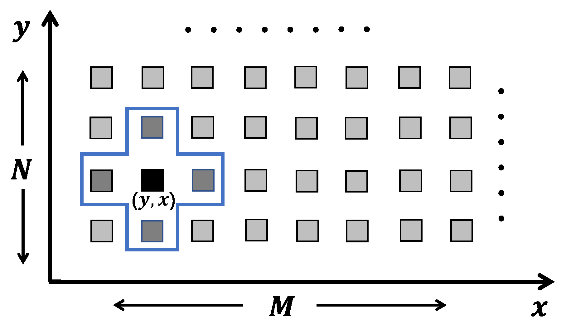
Stencil computations are a class of kernels using the fixed pattern (stencil) to update data elements on a one- or multi-dimensional grid. For example, Figure 1 shows the typical four point stencil kernel for solving the Laplace equation on a 2D () array. We can easily use several lines of high-level C code to describe this kernel in Listing 1.
Listing 1.
High-level code for Laplace equation kernel.

The performance of running stencil-based applications on FPGA depends mainly on the level of parallelism, that is how many stencil operations can the FPGA perform in parallel. The Laplace kernel in Listing 1 includes two types of loops. The outermost loop traverses the time dimension. Unrolling this loop in the target design means that FPGA can execute stencil operations in parallel at different time iterations. This type of parallelism is often referred to as temporal parallelism.
In another case, the inner two loops traverse the 2D space dimension. The target design can unroll these loops along the x-axis, y-axis, or even both axes, which means that the FPGA can simultaneously perform multiple stencil operations at the same time iteration. This type of parallelism is often called spatial parallelism. Aggregate parallelism can be calculated by the product of spatial parallelism and temporal parallelism.
2.2. FPGA with HBM Memory
Compared with computing capabilities, the bandwidth improvement of FPGA memory interfaces is usually unsustainable. For example, the latest Virtex UltraScale Xilinx FPGA has 12k DSP slices, which is six times that of Virtex 6. On the other hand, to increase the memory bandwidth, the most commonly used method is to connect the FPGA to multiple external memory banks, which is often limited by the I/O footprint, energy consumption, or cost issues.
With the development of silicon stacking technology, HBM handles the memory bandwidth problem in another way by packaging the FPGA chip and DRAM chips side-by-side in the same ICpackage. The latest HBM standard (HBM2) allows four or eight DRAM chips to be stacked on top of each other. By adding multiple chips to the same package, the footprint requirement can be significantly reduced. Due to the short wire distance among these chips, HBM can also benefit from the signal transporting and performance improvement.
Our target FPGA, Alveo U280, is integrated with two physical stacks of HBM memory. One HBM stack has 16 memory channels to connect to the FPGA chip. Each channel works similar to a conventional DDR memory bank. The memory controller of HBM channels uses the AXI3bus protocol as the communication interface. Like the DDR bank, a specific channel can only access data in its own memory space. Due to the flexibility of FPGAs, Xilinx overcomes this limitation by introducing an AXI switching network. The network can route memory accesses between different HBM channels and any other AXI buses according to access addresses, thereby giving users complete control over memory allocation.
2.3. Related Work
Generally, the size of the target stencil array is larger than the capacity of the FPGA on-chip memory. Thus, users usually need to store the array in external memory. Applying spatial parallelism requires parallel accesses to the array, i.e., the external memory, which makes the memory bandwidth a bottleneck. Since the external bandwidth of traditional FPGAs is very low, using only the spatial parallelism method on FPGAs cannot fully employ the features of the FPGA architecture. Therefore, few studies have focused on using spatial methods to optimize stencil computations on FPGAs.
On the other hand, exploiting temporal parallelism for implementing stencil computations on FPGAs is very convenient. The FPGA architecture is suitable for building pipeline structures. By using a pipeline structure, users can simultaneously perform stencil operations at different time steps (Figure 2), thereby improving design performance through temporal parallelism and avoiding bandwidth limitations. Many previous significant studies [11,12,13,14,15,16,17] have focused on optimizations in this area, especially in terms of memory partitioning, data reuse, overlap tilling, and design automation.
Among these papers, the research in [11] proposed an HLS design flow for stencil computation with both Synphony C and the Vivado HLS compiler. They exploited temporal parallelism to enhance stencil computation performance and reuse data in their cone-based architecture. However, compared with the sliding window buffer approach, the efficiency of data reuse ability was not optimal. Furthermore, they did not discuss the possible optimization opportunities in the stencil spatial domain.
First, a memory partitioning strategy to solve the concurrent data accesses (data parallelism) problem in FPGA designs was introduced [19]. Later, the authors in [12] optimized such a strategy for stencil computations by using the sliding window buffer. They proved their method could achieve full data reuse with minimum memory resource. They also developed a design automation flow to generate the corresponding structure. However, their research goal mainly was to present the method’s potential and lacked evaluating the performance gains of stencil computation in their benchmarks.
The studies in [14,15] proposed high performance FPGA structures for stencil computations with the Intel OpenCL SDK. Their designs can exploit the ability of data reuse from both spatial and temporal locality by using the shift register-based buffer, i.e., sliding window buffer. Furthermore, they employed overlap tiling to remove the input data size constraint [15]. However, their shift register-based buffer structures were highly dependent on the Intel HLS environment to support the concurrent data accesses, which hurt the design portability. We will show the detailed reasons in the following section.
Instead of using a shift register-based approach, the research in [16,17] chose to construct the window buffer by explicitly using multiple FIFOs and FFs. They connected the window buffers to form a data-flow architecture. Due to bandwidth limitation, they only scaled the buffer design in one spatial dimension, thereby missing the potential optimization opportunities for certain stencil kernels.
3. Stencil Computation Architecture
In this section, we first introduce the sliding window buffer structure and discuss the design scalable parallelism in the spatial dimension with a detailed example. Then, we show the brief overview of our proposed architecture. At last, we present the optimization flow for efficiently using the HBM bandwidth.
3.1. Sliding Window Buffer Design Approaches
The sliding window buffer is a well-known technique for building deep-pipeline structures on FPGAs, and previous papers have already shown the methods of how to use the sliding window buffer to utilize the temporal parallelism of stencil kernels. It has a significant impact on the performance of stencil computations. From the perspective of a high-level language, the sliding window buffer can be regarded as the basic data structure of the stencil kernel. The kernel data access pattern and calculation are mainly based on the design of the sliding window. An appropriate sliding window buffer design can help target the stencil application to achieve better performance with less resource cost. Therefore, our sliding window buffer design objectives can be described as follows:
- The sliding window buffer can exploit the data locality of the target stencil kernel to achieve the full data reuse ability with the minimum memory resource cost.
- The sliding window buffer also has to address the data parallelism, i.e., passing all data inside the stencil window to the computing unit and preparing the required data for the next memory access.
- With the HBM bandwidth support, the scalability of the sliding window buffer can be extended to the entire space dimension of the target stencil kernel.
Another thing that caught our attention is the design portability. One obvious advantage of high-level languages is portability. For HLS, although many different HLS compilers do support using the same language, such as C, C++, or OpenCL, they are more or less dependent on their unique development environment. Since the sliding window buffer plays an important role in the entire stencil computation architecture, our sliding buffer design also seeks to reduce the dependency on a specific HLS compiler.
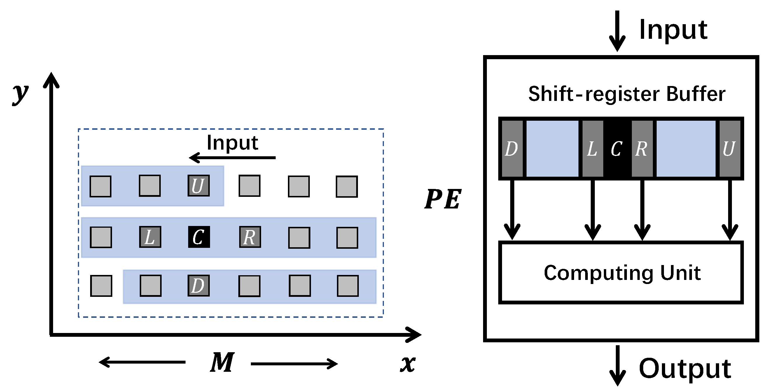
Figure 3 shows the shift register-based sliding window buffer design for the stencil kernel in Figure 1. In each clock cycle, the shift register-based buffer moves the new input data into their head position and removes the used data from the tail position. Meanwhile, the compute cells () inside the stencil window can be directly accessed and transferred to the computing unit through this shift buffer. However, this type of design can only be properly synthesized under the Intel HLS environment. This is mainly determined by the following two reasons:
- The high-level language descriptions of the shift register-based buffer can usually be recognized by the HLS compiler and directly synthesized using the corresponding IP core. The shift register IP [20] in the Intel HLS environment allows users to access in parallel the internal positions (taps) of the shift register in one clock cycle. In contrast, other HLS environments may not support this feature. For example, the corresponding Xilinx IP [21] can only access data at the head or tail of the shift register.
- The HLS compiler often uses block-RAM (BRAM) to store the target stencil array. Performing concurrent memory loads on the BRAM within one clock cycle is limited by the BRAM port number, i.e., the data parallelism issue. The Intel HLS environment can automatically manage the data parallelism issue by utilizing techniques such as redundant BRAMs (memory replication) and/or increasing the BRAM operating frequency (double pumping). These features are closely related to the Intel HLS environment.
In fact, these user-friendly features improve development efficiency by allowing developers to more easily use high-level languages to describe memory hierarchy systems. Meanwhile, this compiler-dependent feature also impairs the portability of the design. In addition, stencil applications often have complex memory access patterns. If the compiler cannot recognize this pattern, it will use hardware resources inefficiently to partition the memory system to solve the data parallelism problem.
Considering the design portability, we suggest that developers should carefully utilize HLS compiler-relevant techniques. For users who do not have a strong background in FPGA, these techniques may prevent them from identifying the performance bottleneck when porting the design to other platforms. To achieve a similar portability level as the high-level language tools on CPUs, the HLS tools on FPGAs still have a long way to go. It needs both academia and industry to continuously contribute to this area, such as standard IP core behaviors, unified compiler pragmas, and memory interface protocols.
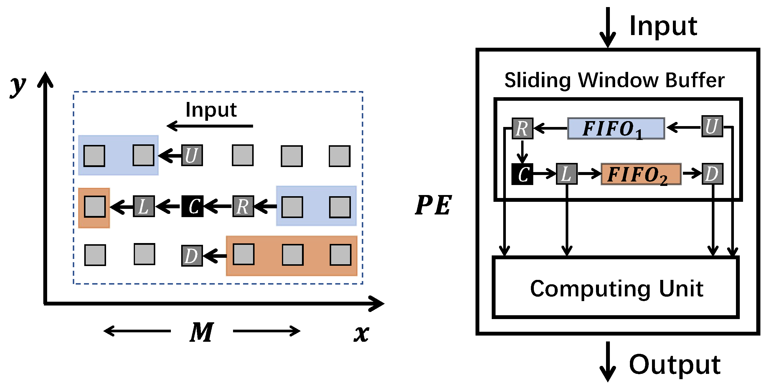
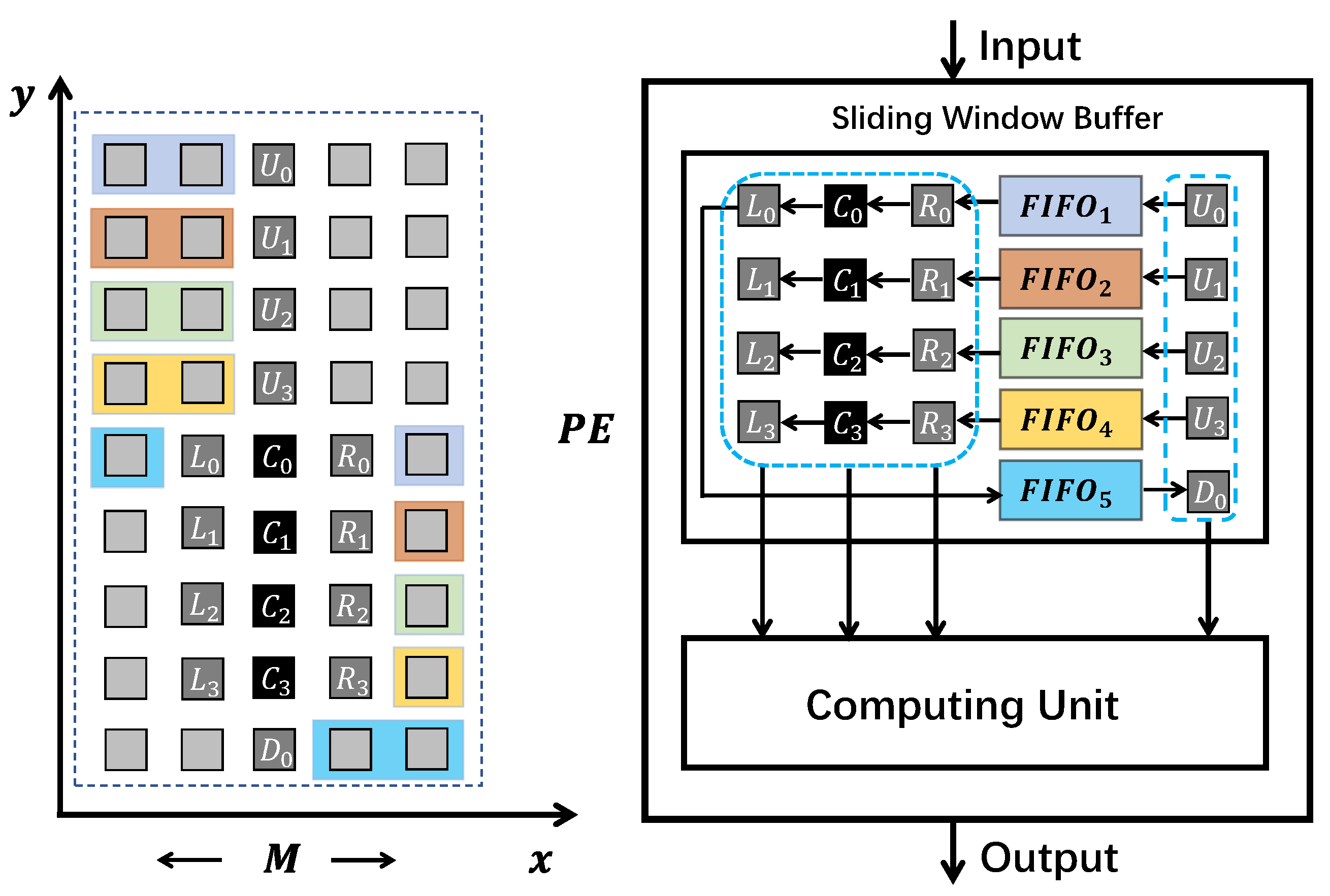
Our sliding window buffer design utilizes the conventional resource types or IP cores in FPGA, such as FIFOs and registers, to clearly describe the behavior of the sliding window buffer structure and solve the data parallelism problem. Figure 4 illustrates the FIFO-based design with the same Laplace stencil kernel. The U register reads data directly from the processing element (PE) input every clock cycle. The registers R and D are ejected from and , respectively. The L register comes from the C register, which bypasses data in the R register. After the computation, the register U is pushed into , and L is pushed into . The computed result goes to the PE output.
The minimum size of the sliding window buffer depends on the maximum data reuse distance [12]. For example, the U cell in the stencil window can be completely reused three times, i.e., when it becomes the R, L, or D cell. The distance between U and D is defined as the maximum reuse distance. In this case, the maximum data reuse distance is , which means that the sliding window buffer needs to store at least cells to achieve full data reuse capability. For the FIFO-based sliding window buffer structure, the FIFOs are mainly responsible for storing and moving data. The registers are used to support concurrent data access.
As we pointed out in Figure 2, utilizing the temporal parallelism of the stencil computations can be implemented by cascading the multiple duplicated PEs to form a deep-pipeline architecture. The most obvious advantage of this approach is that we can improve the stencil performance without increasing the external memory requirements. However, compared with the temporal parallelism method, using spatial parallelism usually shows better resource efficiency. Since increasing the degree of temporal parallelism consumes multiple replicated PEs to perform stencil operations in different time steps, for the spatial parallelism approach, multiple stencil operations are performed at the same time step, i.e., inside one PE, which allows developers to find more resource sharing and reuse opportunities. The drawback of this approach is that it requires the support of external bandwidth.
Now, with the benefits of HBM memory, we can equally employ spatial and temporal parallelism approaches to improve stencil design performance. Thus, to efficiently exploit the optimization opportunities on the spatial approach, we propose the scalable sliding window buffer design approaches in the following three cases. For simplicity, we still use the Laplace equation as the target stencil kernel.
3.1.1. Scaling along the x Dimension of the Target Stencil Space
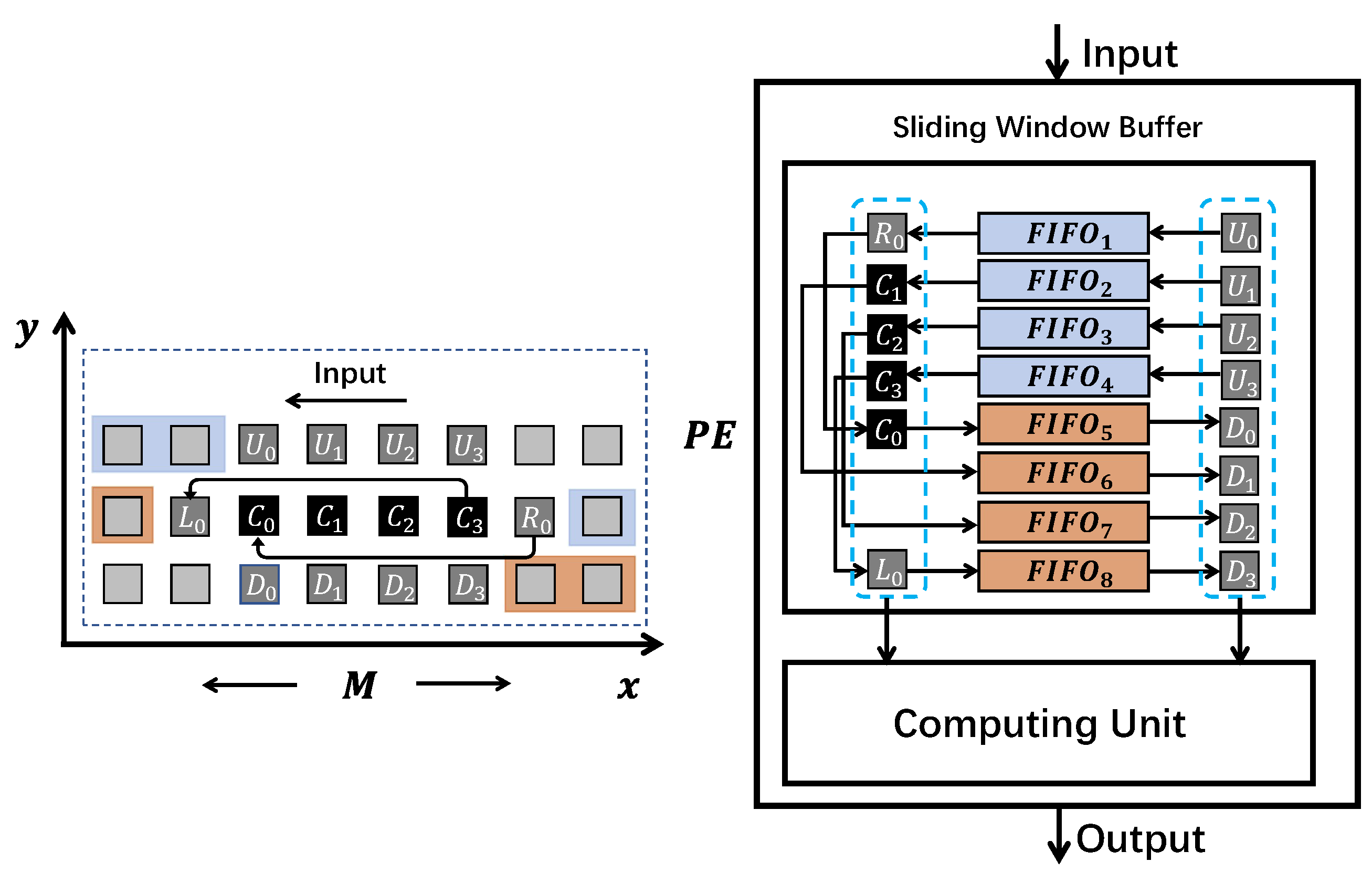
We unroll the loop along the x dimension (the most inner loop in Listing 1) to exploit spatial parallelism. For example, suppose we set the unrolling parameter to four, which means that four stencil operations at the same time step are executed simultaneously inside one PE. To achieve our sliding buffer design objectives, we show the scalable FIFO-based buffer design in Figure 5. The sliding window buffer is mainly constructed by eight FIFOs and 14 registers. It works as follows:
- In every clock cycle, the up floor registers ( to ) read four fresh cells in the stencil array x dimension from the input;
- Registers , , , and are popped from to , respectively. and reuse cells’ data in and ;
- Down floor registers to are popped from to . Then, all 14 registers are ready to be passed to the computing unit for performing four stencil operations in parallel.
- After the computations, results in positions , , , are transferred to the output. to are pushed into to , respectively. is pushed to and , , and to , , and .
This sliding window buffer design can be easily scaled to other unrolling parameter values along the x dimension of the stencil space. The registers in the sliding window buffer are responsible for solving the data parallelism issue. The structure of registers depends on the target stencil window shape and the unrolling parameter. The number of total registers can be defined as:
where represents the number of cells in one stencil window. is the target unrolling parameter value. means the number of cells in the overlap area of consecutive stencil windows along the x dimension.
The FIFOs in the sliding window buffer are responsible for updating the registers and store the used data for achieving full data reuse ability. To cooperate with the registers, we need at least FIFOs. represents the number of FIFOs. It can be calculated by using the unrolling parameter and the the “height” of the stencil window, which is defined as:
where is the target stencil window’s “height”. In the case of Laplace stencil application, the equals two.
As we previously mentioned in this section, to achieve full data reuse, the minimum size of the sliding window buffer is decided by the data reuse distance. We can extend the basic data reuse distance definition to our scalable sliding window buffer design. For example, similar to Figure 4, the maximum data reuse distance in Figure 5 is between and , that is . Our scalable window buffer size can be calculated as:
where M is the x dimension length in the target stencil space. In this case, our sliding window buffer size is , which means our buffer design can achieve full data reuse with the minimum buffer size.
The significant advantage of scaling in the x dimension is the memory resource consumption of the sliding window buffer. In Figure 4, the buffer stores stencil cells to perform one stencil operation. Suppose we only use temporal parallelism to achieve the same performance as in Figure 5. We need four replicated PEs, including four sliding window buffers, and they need to store stencil cells. In Figure 5, by utilizing spatial parallelism, our sliding window buffer only needs to store stencil cells.
3.1.2. Scaling along the y Dimension of the Target Stencil Space
For a 2D stencil array space (e.g., Listing 1), besides unrolling in the x dimension, we also can increase the spatial parallelism by unrolling the loop in the y dimension. We use the same conditions as unrolling in the x dimension to analyze this situation. The detailed sliding window buffer design is shown in Figure 6.
Since this sliding window buffer operates similar to that in Figure 5, for the sake of simplicity, we omit the detailed workflow description. Compared with scaling along the x dimension, this type of sliding window buffer design has the obvious defect of memory resource consumption. The sliding window buffer size in Figure 6 can be calculated as:
In Figure 6, the sliding window buffer size is equal to . Unlike the previous design, the sliding buffer size grows linearly with the unrolling parameter . Furthermore, we can also convert this type of sliding buffer design to the former one through a loop interchange. Therefore, it is not common to increase the degree of spatial parallelism by only unrolling the loop in the stencil space y dimension.
3.1.3. Hybrid Scaling Strategy
The hybrid scaling strategy combines the above two situations. The spatial parallelism parameter of a 2D stencil space can be implemented by any combinations of (i.e., scaling in the x dimension) and (i.e., scaling in the y dimension) as long as they satisfy . In fact, the above two scaling strategies (along the x or y dimension) can also be regarded as two special cases of this hybrid unrolling strategy, that is when or , respectively. Figure 7 presents a specific sliding window buffer design under the condition that and are both two.
We also omit the detailed workflow description here. Through the above analysis, we know that the sliding window buffer size has a linear relationship with the parameter and little to do with the parameter . We can use the following formula to calculate the buffer size in the hybrid unrolling strategy.
The sliding window buffer size in Figure 7 is equal to . Compared with the buffer design scaling only in the x dimension, this hybrid scaling buffer design is inferior in terms of buffer size. However, this hybrid design provides opportunities to reuse the computing resource (e.g., DSPs) in the FPGA. For example, for computing the result in position , the computing unit need to perform the stencil operation as . Similar to , for performing the stencil operations of position , we calculate the result of . Thus, inside the computing unit, the temporal result of can be reused twice. As a consequence, this hybrid scaling sliding window buffer design can provide extra design choices, which allow certain stencil applications to achieve optimal performance.
In summary, the three scaling window buffer design strategies described above can be generalized to the 3D stencil array or even higher dimensional spaces. The design combinations of these strategies mainly depend on the value of the spatial parallelism parameter . The maximum value of is decided by the bandwidth peak of external memory. A larger bandwidth (e.g., FPGA with HBM) will broaden the sliding window buffer design space, allowing developers to find an appropriate solution to obtain the expected performance of target stencil application.
3.2. Proposed Architecture Overview
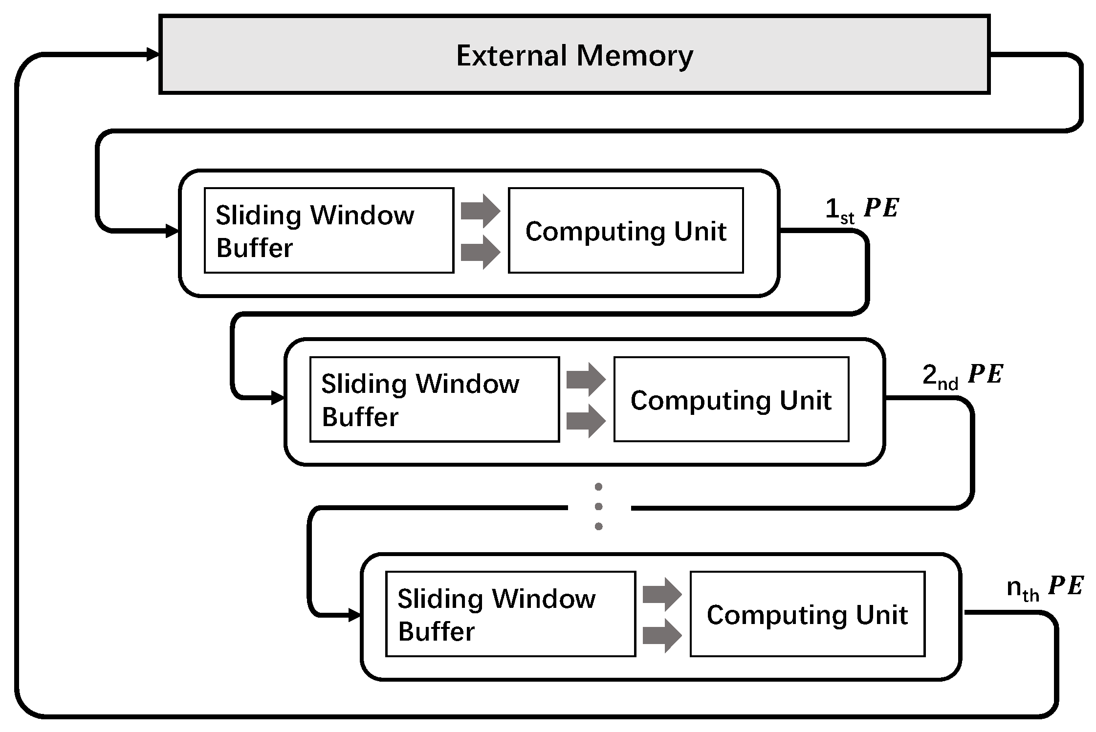
In our stencil computation architecture, we scale-up the stencil kernel performance by using both spatial and temporal parallelism. The overview of our proposed architecture is presented in Figure 8. The processing element (PE) is responsible for performing multiple stencil operations in one time iteration, i.e., utilizing spatial parallelism to increase the stencil computation performance. The structure of PE is mainly composed of the sliding window buffer and the computing unit. In every clock cycle, the sliding window buffer reads data from the input and prepares the corresponding registers for the computing unit. The computing unit generates the computed results to the output. All PEs are identical structures for one specific stencil application. The input of each PE can either directly come from external memory or the previous PE, and the output can go to the next PE or external memory. We link the multiple PEs together to form a deep-pipeline architecture to utilize temporal parallelism.
In the HLS environment, we can describe the behavior of PE inside a function. The function input/output can be defined as the FIFO type, which was not originally supported in software-based languages (e.g., C). Currently, many popular HLS compilers have their own custom data type to declare the function interface as the FIFO structure such as hls::stream for Xilinx, ihc::stream for Intel, or channel in OpenCL. Using the custom FIFO data type will help HLS compilers to identify the declared variable or interface to instantiate the appropriate IP core into the architecture.
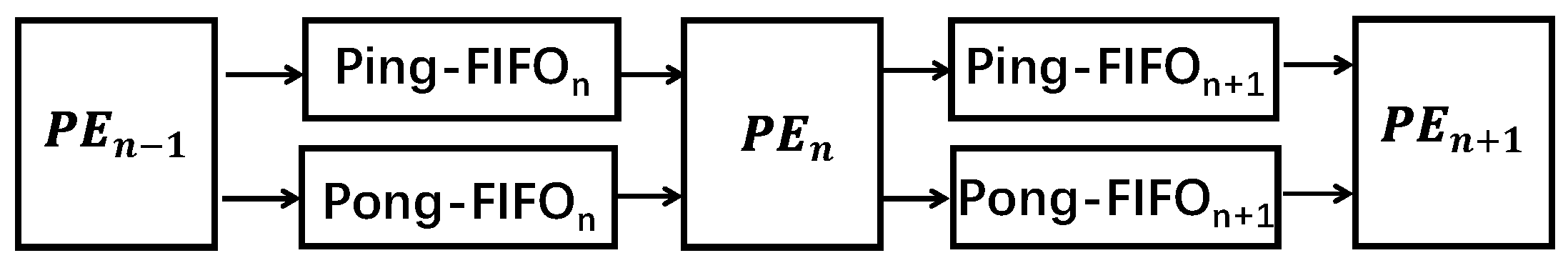
To achieve the full pipeline in the entire stencil architecture, we employ the double buffer scheme (ping-pong buffer), as shown in Figure 9. In the first clock cycle, the input data of a PE come from the corresponding ping-FIFO and the output data are written to the next level pong-FIFO. In the next clock cycle, the situation runs in the opposite manner. The double buffer scheme is a wildly used design technique to avoid stalls in a pipelined architecture. The Xilinx HLS compiler even has developed the special pragma, i.e., pragma dataflow, for using the double buffer scheme. The developers under the Xilinx HLS environment can use the pragma dataflow to declare a dataflow region. The functions inside this region will be automatically connected via the double buffer structure. However, as we stated before, these “pragmas” depend heavily on the particular HLS compiler, which improve the development efficiency, but sacrifice portability.
3.3. HBM Memory Bandwidth Optimization
Compared to modern GPUs, even for HBM-enabled FPGAs, the memory bandwidth is not an advantage. In addition, the GPU has an efficient dedicated memory controller that can manage memory access requests from thousands of GPU cores. The controller can implicitly merge these memory accesses to take full advantage of the GPU’s external memory bandwidth. However, in terms of FPGAs, users need to configure such memory controllers themselves. Using an inappropriate configuration will result in extremely low bandwidth utilization.
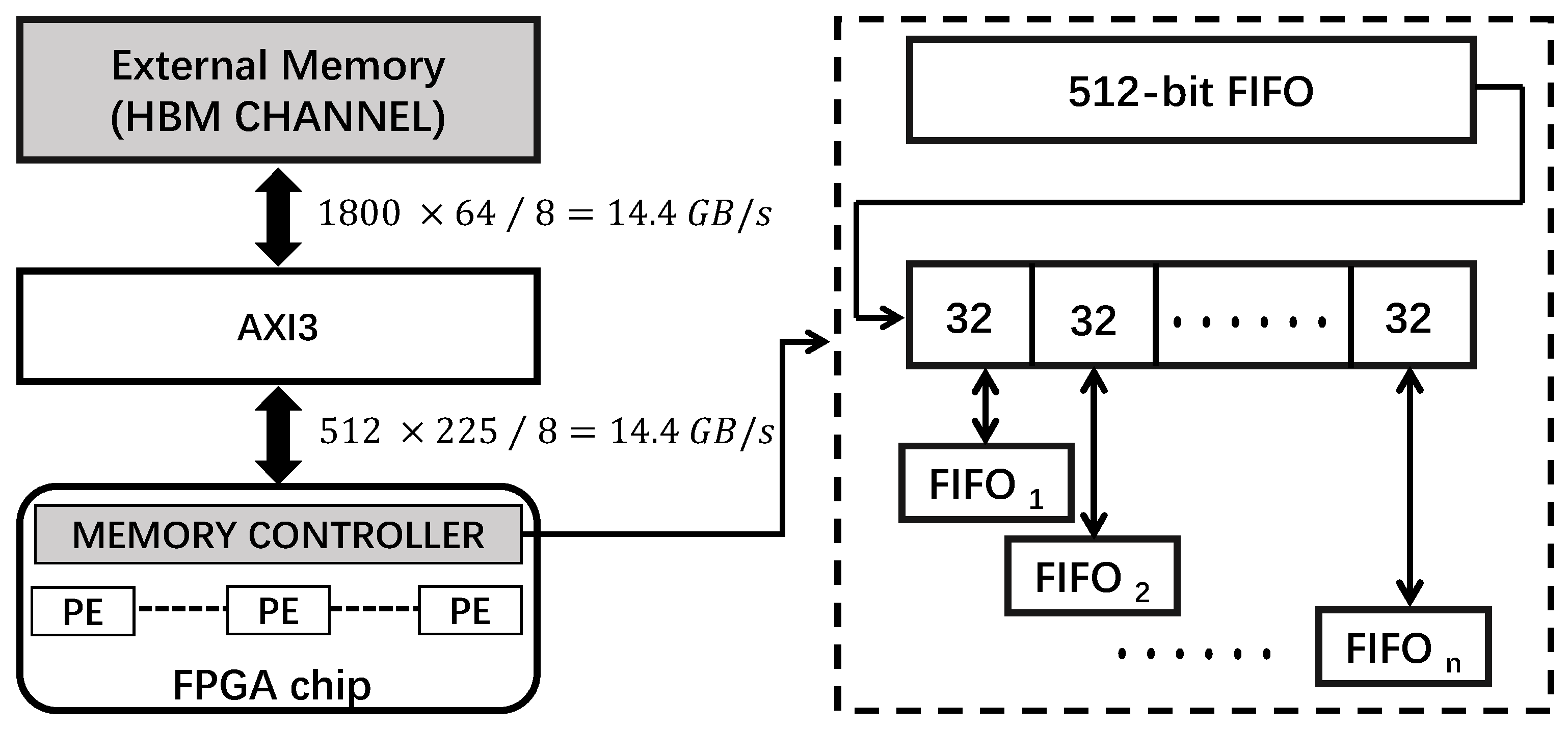
We use a detailed example in Figure 10 to illustrate the proposed memory controller design. Usually, compared to using the HDL development method, we cannot control the memory interface in detail in the HLS environment. The FPGA chip is connected to external storage (e.g., HBM) via the AXI bus. To reach the full utilization of HBM memory, our HLS memory controller configuration needs to meet the following requirements:
- First, we need to increase the data width of the memory interface in the FPGA side due to the low operating frequency of FPGAs, e.g., 300 MHz or lower. Assume HBM memory stacks are configured to operate at 900 MHz. For the Alveo U280 FPGA board, it is connected to two stacks HBM memory, and each stack has 16 channels. The peak performance of one HBM channel can be calculated as 900 MHz × 2 × 64/8 = 14.4 GB/s. Suppose our FPGA chip runs at 225 MHz. To fully use the HBM peak memory bandwidth, we have to manually coalesce data into a 512 bit width, i.e., 512 × 225/8 = 14.4 GB/s
- Second, we use the burst mode of the AXI bus as much as possible.
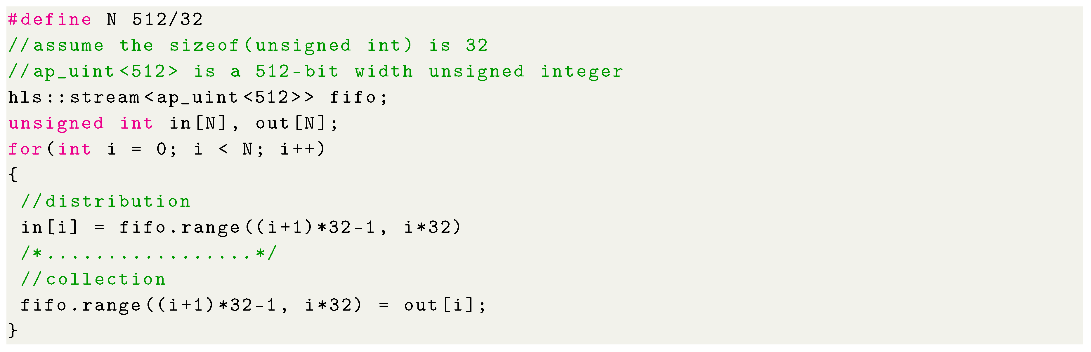
We address the first issue by building a data distribution and collection buffer. When writing data to the external memory, this buffer collects multiple primitive data (e.g., 32-bit) and coalesces them into a large data width (e.g., 512 bit). On the other side, the buffer cuts large width data into multiple small width data when performing read operations. We implement this buffer mainly relying on a large width FIFO. In the HLS compiler, we can use an arbitrary integer type to synthesize a FIFO with a custom width. We use the pseudo-code below (Listing 2) to explain the idea in detail.
Listing 2.
Custom data width FIFO structure.

One essential thing to be noted here is that the large width integer type (e.g., ) only helps the HLS compiler synthesize the FIFO structure into the proper (512 bit) width; it does not mean that the FIFO needs to be filled only with the integer data type. For example, we also can coalesce 16 32 bit float data into a 512 bit width FIFO. In this case, we need to perform a special data type conversion first as following (Listing 3).
Listing 3.
Data type conversion between integer and float.

The second requirement is mainly achieved by the full pipelined architecture and the AXI bus. Our stencil architecture can be fully pipelined, i.e., it performs read and write operations to external memory in every cycle. The burst-based mode of AXI has a higher transmission efficiency by only issuing the start address and then bursting data transfer in every clock cycle. The receiver adjusts the address changes for each subsequent transfer under the burst-based mode. We need to follow some special programming patterns or use the proper pragma to configure the AXI bus. For example, in Xilinx, sequential writes or reads inside a “for” loop can be inferred to a memory burst access. The burst length is configured by pragma “interface m_axi”. In the Intel OpenCL environment, there is a load-store unit that automatically buffers memory access requests until the largest possible burst can be made. In short, the configuration of I/O interface is very dependent on the HLS environment, which leads to poor portability in this area.
4. Performance Model
In this section, we introduce a performance model of our stencil architecture, which can aid the developer to select the suitable design parameters for a target stencil application. For performing i time iteration stencil operations on an n-dimensional stencil array , the total workload can be calculated as:
where means the maximum length in one array dimension. Our stencil architecture can utilize both spatial and temporal parallelism, and the aggregate degree of parallelism can be calculated as:
The spatial parallelism degree is equal to the value of the unrolling parameter (). Our sliding window buffer design can support multi-dimensional unrolling strategies. On the other hand, the temporal parallelism is realized by the deep-pipeline architecture, i.e., the number of PEs (). The proposed stencil architecture is able to achieve a full pipeline without stalls. Then, the peak throughput can be computed as:
where is the stencil architecture throughput (cells/s) and represents the stencil kernel frequency.
However, Equation (10) does not include the initialization phase of the deep-pipeline stencil architecture, which is the period from when the stencil architecture receives its first input until it produces the first output. We use the following equation to calculate the cost of the initialization phase:
where is the pipeline stage steps of one single stencil PE. Finally, The executing time of stencil computation () is calculated in:
The performance of our stencil architecture mainly depends on two design parameters ( and ). The selections of these two parameters are constrained by:
where means the maximum hardware resources of a certain FPGA chip, is the resources consumption for implementing the stencil architecture, and represents the platform resource cost such as the HBM memory controller IP, PCIe IP. The resources of the stencil architecture are mainly consumed by PEs. The resources cost of one PE is primarily composed of the sliding window buffer () and the computing unit (). As we analyzed earlier, the maximum value of is also limited by the peak performance of the HBM memory bandwidth (). It can be defined as:
where is the width of the target data type.
In our stencil architecture, we mainly rely on tuning two design parameters, i.e., and , to adjust the design performance. We explain the parameter tuning process by using the roof-line model in Figure 11. The y axis represents the FPGA performance. The maximum attainable performance of an FPGA is determined by the computing resource . The x axis means the number of PEs . The maximum value of is limited by the peak external memory bandwidth .
Then, the parameter tuning process can be described as follows:
- Calculate the maximum value of parameter by using the peak memory bandwidth .
- Keep the value of to explore the value of , until we reach to the maximum computing resource limitation.
- Add the design parameters into our parameter tuning area.
- Decrease the value of , e.g., to a smaller value , and repeat the above steps from Step 2.
- The parameter tuning area will end up in, e.g., point . At this point, we also reach the maximum maximum memory resource limitation
Compared to utilizing spatial parallelism, using a large value of temporal parallelism (e.g., the value of ) consumes more memory resources. Assuming we continue to reduce the spatial design parameter to , the target stencil architecture will exhaust all memory resources inside the FPGA before we reach the maximum computing resource limitation. At last, we explore the design parameters inside the parameter tuning area to select the appropriate combination of spatial design parameter and temporal design parameter until the expected performance is obtained.
5. Results
5.1. Experiment Setup
We used the Xilinx Alveo U280 board to evaluate the results. The specifications of the FPGA chip are shown in Table 1. The U280 board is equipped with two stacks of 4GB HBM memory. They connect to the host computer through the PCIe Gen3 interface. The host was an Intel i9900k server with 64 GB memory. The boards work under a Linux (Ubuntu 2018.2) operating system. The Xilinx Vitis 2019.2 was the experiment HLS environment. The target HLS compiler supports using high-level languages such as C, C++, SystemC, or OpenCL to synthesize the stencil kernel.
We chose three benchmarks from various application areas to evaluate our stencil computation architecture. The Sobel 2D filter is a popular edge detection application used in computer vision. The Laplace equation is a typical kernel of the partial differential equations. The Himeno 3D benchmark is developed to evaluate the performance of fluid simulations.
One thing to be noted here is that we did not use all the FPGA hardware resources to evaluate these benchmarks. The FPGA chip in Alveo U280 utilizes a multi-dice technique, called super logic regions (SLRs), to increase the total resource of the FPGA chip. For example, the FPGA chip of the U280 FPGA board has three dice (SLRs). We only assign our stencil architecture to one die. Although all three dice can be used in our experiments, the benchmark performance will be severely affected by the die-crossing connections. As a result, the real bottleneck of our stencil benchmarks is limited by the die-crossing resource, i.e., the super long line (SLL) routing resource in Xilinx. The optimization of SLL is not the purpose of this article.
5.2. Experiment Performance
Table 2 shows the performance results of Sobel 2D. The input image size is 8k (). The Sobel 2D filter can be treated as a special stencil application that only performs one time iteration computation. As a result, we can only employ spatial parallelism in this application. Therefore, this benchmark is actually bounded by the memory bandwidth. In [16], their device was connected to two DDR3-1600 memory banks, which limited their design maximum spatial parallelism degree to 32 ( 250 = 12.8 GB/s). Compared to the Intel Xeon E5-2620 CPU with 4 DDR4 banks, the performance of ADM-PCIE-KU3 boards suffers from the external bandwidth and cannot demonstrate the advantages of the FPGA structure. With the help of HBM memory, our Sobel 2D benchmark performance can reach 77 GCell/s by using the 16 bit data type. For pictures with the eight bit data type, the performance can be improved to 128.4 GCell/s. In addition, we also performed a comparative experiment by using the regular DRAM on the Alveo U280 board. Without the support of HBM, the state-of-the-art Alveo U280 board shows similar performance result as ADM-PCIE-KU3.
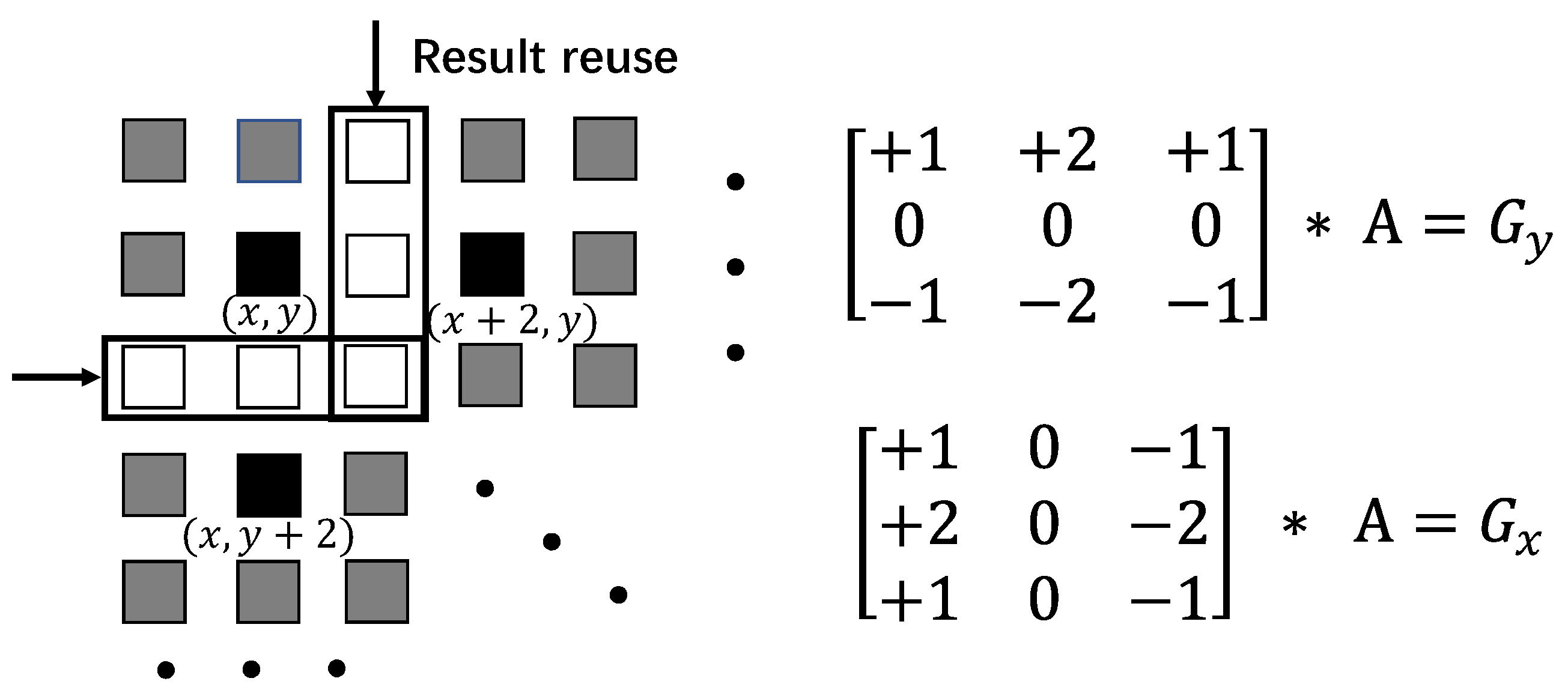
For spatial parallelism , we implemented the Sobel 2D kernel with four different sliding window buffer scaling strategies, i.e., . Figure 12 shows the resource consumption of these four implementations. Since the Sobel 2D benchmark costs no DSP resource, we omit the DSP usage in this figure. Due to some calculations of one stencil cell being able to be reused by other cells (shown in Figure 13), our hybrid strategies can exploit this to adjust the computing and memory resource consumption. The design presents the best resource usage of LUTs. However, in terms of buffer size, this sliding widow’s buffer scaling is eight in the y dimension, which costs the most BRAM bits.
Table 3 shows the performance result of the Laplace equation benchmark. We used the input array size (16,384 × 16,384) for this benchmark. The Laplace benchmark is based on the floating-point operations. Due to external bandwidth limitations, the design parameters of spatial parallelism () in both papers [14,16] was limited to eight. They mainly improved the stencil performance by employing temporal parallelism. In our implementation, we can use 64 (HBM connected) and eight (DRAM connected) as our spatial parallelism design parameters. In addition, we use two different combinations of and to implement the Laplace stencil kernel for the HBM experiment. Increasing the to two provides an extra optimization opportunity for reusing the calculated results in the computing unit of the PE (as we stated in Section 3.1.3).
One thing that deserves our attention is the frequency (). A simple way to improve FPGA performance is to increase the clock frequency. Compared with the work [14], our FPGA clock frequency is inferior. In addition to resource utilization, is also affected by the routing resources inside FPGA. Unlike CPUs or GPGPUs, the FPGA architecture needs to link hardware resources with the routed wires. The lack of routing resources can cause congestion problems, which limits . In the worst case, the design will fail during the routing phase. Compared with the HDL development method, users often cannot describe the FPGA hardware design in detail by using the HLS tools, such as explicitly adding pipeline stages on the critical path. However, we can still reduce congestion areas by optimizing compiler settings or changing the programming patterns. These methods are beyond the scope of this article, and we will leave them for future research.
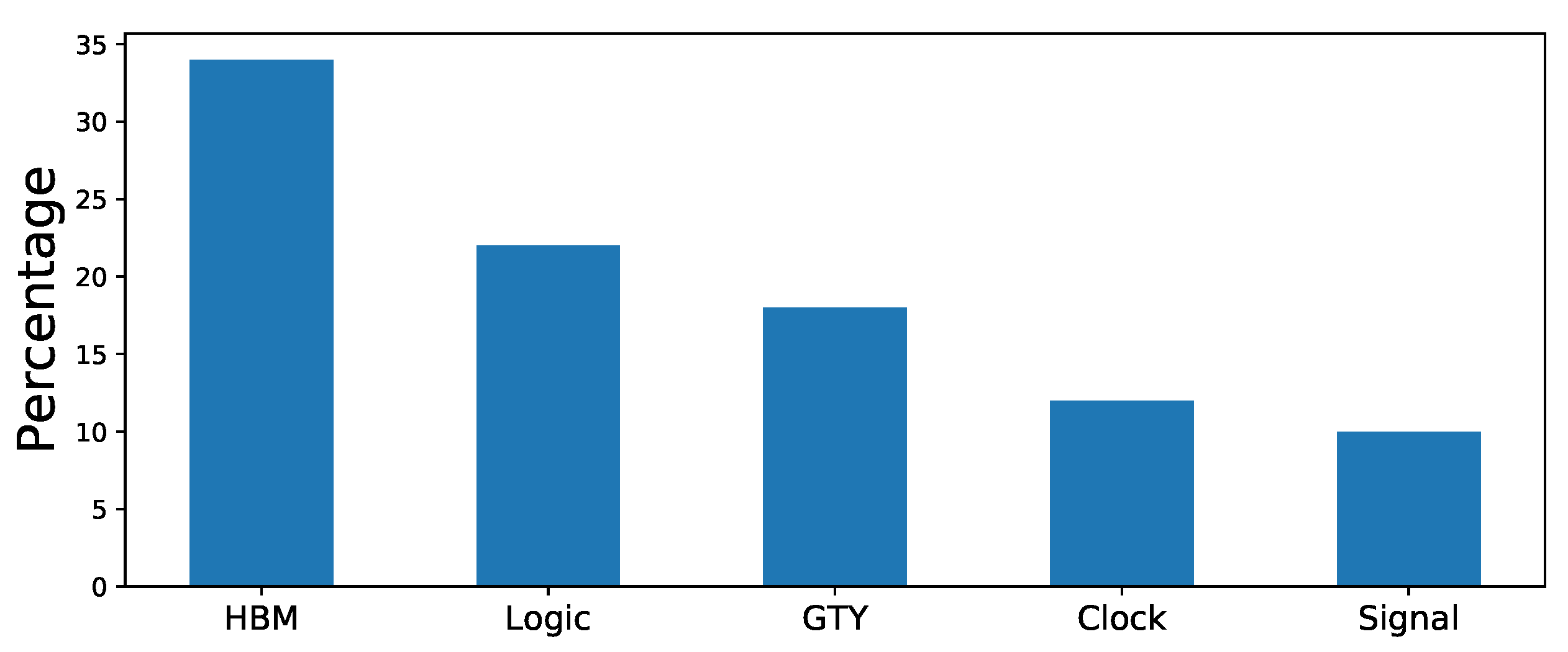
Figure 14 presents the power report generated by the Vivado implementation tool. We use the default junction temperature 37.9 °C. The total on-chip power is 30.83 W. This figure lists the top five power consumption elements inside the FPGA chip. The HBM memory costs the most power budget, i.e., . The logic part including LUTs, BRAMs, and DSPs takes . The rest of the elements, GTY, clock, and signal, use almost .
To verify the proposed stencil architecture in 3D space, we chose the Himeno benchmark as our target application. The Himeno benchmark is a popular program to evaluate the performance of incompressible fluid analysis. A detailed description of the computation kernel can be seen in [22]. The target input array size is . In the 2D stencil computation, the sliding window buffer needs to cache several 1D lines of the 2D input array. For 3D stencil computation, the sliding window buffers need to store more data, that is several 2D planes of the 3D input array, which often makes the memory resources a performance bottleneck. For example, the BRAM resources inside the Alveo U280 can only allow us to use four as the maximum temporal parallelism (). Employing spatial parallelism, specifically scaling the sliding window buffer along the x dimension, can save the memory resources. Through HBM memory, we are able to use 16 as our spatial design parameter (in Table 4). As a result, our performance reached GCell/s, which is 10 times more than the result in [23] and four times more than the DRAM experiment.
6. Conclusions
In this paper, we present an HLS-based architecture design for implementing stencil computations on HBM-ready FPGAs. With the help of HBM memory, our proposed architecture can improve the FPGA performance by utilizing both the spatial and temporal parallelism of stencil kernels. We specifically analyze the sliding window buffer scaling strategies in various spatial dimensions. In addition, We also consider the design portability to help users move our stencil architecture to other HLS environments. At last, the results show that our Alveo U280 FPGA board can achieve 128.4 GCell/s in the Sobel 2D benchmark with the eight bit integer data type, 56.6 GCell/s in the Laplace equation with the float data type, and 6.8 GCell/s in the Himeno 3D benchmark. In future research, we want to develop a tool that can automatically generate the HLS code of stencil kernels by only specifying several key design parameters. We also plan to discuss the guidelines for reducing the routing congestion area with the HLS development approach.
Author Contributions
Conceptualization, C.D. and Y.Y.; methodology, C.D.; software, C.D.; formal analysis, C.D.; investigation, C.D.; resources, Y.Y.; writing, original draft preparation, C.D.; writing, review and editing, C.D. and Y.Y.; supervision, Y.Y.; project administration, Y.Y.; funding acquisition, Y.Y. All authors read and agreed to the published version of the manuscript.
Funding
This work was supported in part by MEXT through the Next Generation High-Performance Computing Infrastructures and Applications R&D Program (Development of Computing-Communication Unified Supercomputer in Next Generation) and by JSPS KAKENHI Grant Numbers JP17H01707 and JP18H03246.
Acknowledgments
The authors would like to thank Xilinx Inc. for providing the FPGA software tools through the Xilinx University Program.
Conflicts of Interest
The authors declare no conflict of interest.
References
- Caulfield, A.M.; Chung, E.S.; Putnam, A.; Angepat, H.; Fowers, J.; Haselman, M.; Heil, S.; Humphrey, M.; Kaur, P.; Kim, J.Y.; et al. A cloud-scale acceleration architecture. In Proceedings of the 49th Annual IEEE/ACM International Symposium on Microarchitecture, Taipei, Taiwan, 15–19 October 2016; pp. 1–13. [Google Scholar]
- Vanderbauwhede, W.; Benkrid, K. High-Performance Computing Using FPGAs; Springer: Berlin, Germany, 2013. [Google Scholar]
- Vivado High-Level Synthesis. Available online: https://www.xilinx.com/products/design-tools/vivado/integration/esl-design.html (accessed on 6 May 2020).
- Intel High Level Synthesis Compiler. Available online: https://www.intel.com/content/www/us/en/software/programmable/quartus-prime/hls-compiler.html (accessed on 6 May 2020).
- Canis, A.; Choi, J.; Aldham, M.; Zhang, V.; Kammoona, A.; Anderson, J.H.; Brown, S.; Czajkowski, T. LegUp: High-level synthesis for FPGA-based processor/accelerator systems. In Proceedings of the 19th ACM/SIGDA International Symposium on Field Programmable Gate Arrays, Monterey, CA, USA, 27 February–1 March 2011; pp. 33–36. [Google Scholar]
- Grunau, D.; Chen, S.; Eggert, K. A lattice Boltzmann model for multiphase fluid flows. Phys. Fluids 1993, 5, 2557–2562. [Google Scholar] [CrossRef] [Green Version]
- Sano, K.; Yamamoto, S. FPGA-Based Scalable and Power-Efficient Fluid Simulation using Floating-Point DSP Blocks. IEEE Trans. Parallel Distrib. Syst. 2017, 28, 2823–2837. [Google Scholar] [CrossRef]
- Ramahi, O.M. The concurrent complementary operators method for FDTD mesh truncation. IEEE Trans. Antennas Propag. 1998, 46, 1475–1482. [Google Scholar] [CrossRef] [Green Version]
- Hegarty, J.; Brunhaver, J.; DeVito, Z.; Ragan-Kelley, J.; Cohen, N.; Bell, S.; Vasilyev, A.; Horowitz, M.; Hanrahan, P. Darkroom: Compiling high-level image processing code into hardware pipelines. ACM Trans. Graph. 2014, 33, 144–151. [Google Scholar] [CrossRef]
- Alan, C. Bovik. In The Essential Guide to Image Processing; Academic Press: New York, NY, USA, 2009. [Google Scholar]
- Nacci, A.A.; Rana, V.; Bruschi, F.; Sciuto, D.; di Milano, P.; Beretta, I.; Atienza, D. A high-level synthesis flow for the implementation of iterative stencil loop algorithms on FPGA devices. In Proceedings of the 50th ACM/EDAC/IEEE Design Automation Conference (DAC), Austin, TX, USA, 2–6 June 2013. [Google Scholar]
- Jason, C.; Peng, L.; Bingjun, X.; Zhang, P. An Optimal Microarchitecture for Stencil Computation Acceleration Based on Non-Uniform Partitioning of Data Reuse Bufers. IEEE Trans. Comput. Aided Des. Integr. Circuits Syst. 2015, 35, 407–418. [Google Scholar]
- Natale, G.; Stramondo, G.; Bressana, P.; Cattaneo, R.; Sciuto, D.; Santambrogio, M.D. A polyhedral model-based framework for dataflow implementation on FPGA devices of Iterative Stencil Loops. In Proceedings of the 2016 IEEE/ACM International Conference on Computer-Aided Design (ICCAD), Austin, TX, USA, 7–10 November 2016; pp. 1–8. [Google Scholar]
- Waidyasooriya, H.M.; Takei, Y.; Tatsumi, S.; Hariyama, M. OpenCL-Based FPGA-Platform for Stencil Computation and Its Optimization Methodology. IEEE Trans. Parallel Distrib. Syst. 2017, 28, 1390–1402. [Google Scholar] [CrossRef]
- Zohouri, H.R.; Podobas, A.; Matsuoka, S. Combined Spatial and Temporal Blocking for High-Performance Stencil Computation on FPGAs Using OpenCL. In Proceedings of the 2018 ACM/SIGDA International Symposium on Field-Programmable Gate Arrays, Monterey, CA, USA, 25–27 February 2018; pp. 153–162. [Google Scholar]
- Chi, Y.; Cong, J.; Wei, P.; Zhou, P. SODA: Stencil with optimized dataflow architecture. In Proceedings of the 2018 IEEE/ACM International Conference on Computer-Aided Design (ICCAD), San Diego, CA, USA, 5–8 November 2018; pp. 1–8. [Google Scholar]
- Reggiani, E.; Natale, G.; Moroni, C.; Santambrogio, M.D. An FPGA-Based Acceleration Methodology and Performance Model for Iterative Stencils. In Proceedings of the 2018 IEEE International Parallel and Distributed Processing Symposium Workshops (IPDPSW), Vancouver, BC, Canada, 21–25 May 2018; pp. 115–122. [Google Scholar]
- Alveo U280 Data Center Accelerator Card. Available online: https://www.xilinx.com/products/boards-and-kits/alveo/u280.html (accessed on 6 May 2020).
- Wang, Y.; Li, P.; Zhang, P.; Zhang, C.; Cong, J. Memory partitioning for multidimensional arrays in high-level synthesis. In Proceedings of the 50th Annual Design Automation Conference, New York, NY, USA, 29 May 2013; pp. 1–6. [Google Scholar]
- RAM-Based Shift Register IP Core. Available online: https://www.intel.com/content/dam/www/programmable/us/en/pdfs/literature/ug/ug_shift_register_ram_based.pdf (accessed on 6 May 2020).
- RAM-based Shift Register. Available online: https://www.xilinx.com/products/intellectual-property/ram-based_shift_register.html (accessed on 6 May 2020).
- Himeno Benchmark. Available online: http://accc.riken.jp/en/supercom/documents/himenobmt/ (accessed on 6 May 2020).
- Firmansyah, I.; Changdao, D.; Fujita, N. FPGA-based Implementation of Memory-Intensive Application using OpenCL. In Proceedings of the 10th International Symposium on Highly-Efficient Accelerators and Reconfigurable Technologies (HEART), Nagasaki, Japan, 6–7 June 2019; pp. 1–4. [Google Scholar]
Figure 1.
Example of a four point stencil window on a () 2D space.

Figure 2.
Pipeline structure using temporal parallelism. PE, processing element.

Figure 3.
Shift register-based sliding window buffer design for the Laplace stencil kernel.

Figure 4.
FIFO-based sliding window buffer design for the Laplace stencil kernel.

Figure 5.
Example of a scalable sliding window buffer design along the stencil space x dimension.

Figure 6.
Example of a scalable sliding window buffer design along the stencil space y dimension.

Figure 7.
Example of a 2D hybrid sliding window buffer design.

Figure 8.
Overview of the stencil computation architecture.

Figure 9.
Ping-pong FIFOs connections with PEs.

Figure 10.
Memory controller design.

Figure 11.
Performance roof-line model.

Figure 12.
Resource consumption for the Sobel 2D benchmark.

Figure 13.
Computing results for reuse in the Sobel 2D benchmark.

Figure 14.
Power report for Laplace equation benchmark.


Table 1.
FPGA chip specifications.
| Devices | LUT(K) | FF(K) | DSP Slices | Block RAM | HBM Bandwidth |
|---|---|---|---|---|---|
| Alveo U280 | 1303 | 2607 | 9024 | 4032 | 460.8 GB/s |
Table 2.
2D Sobel benchmark performance result.
| Devices | Performance | Frequency | Data Type | ||
|---|---|---|---|---|---|
| (GCell/s) | (MHz) | ||||
| Alveo U280 | 384 | 1 | 77.6 | 240 | uint16_t |
| 640 | 1 | 128.4 | 237 | uint8_t | |
| Alveo U280 with DRAM | 32 | 1 | 5.8 | 246 | uint16_t |
| ADM-PCIE-KU3 [16] | 32 | 1 | 5.37 | <250 | uint16_t |
| Intel Xeon E5-2620 [16] | - | - | 6.66 | 2400 | uint16_t |
Table 3.
Laplace equation benchmark performance result.
| Devices | Performance | Frequency | Data Type | ||
|---|---|---|---|---|---|
| () | (GCell/s) | (MHz) | |||
| Alveo U280 | 4 | 56.6 | 234 | float | |
| 4 | 54.5 | 227 | float | ||
| Alveo U280 with DRAM | 8 | 18 | 31.2 | 240 | float |
| ADM-PCIE-KU3 [16] | 8 | 10 | 18.01 | <250 | float |
| DE5 [14] | 8 | 21 | 45.25 | 283 | float |
Table 4.
Himeno benchmark performance result.
| Devices | Performance | Frequency | Data Type | ||
|---|---|---|---|---|---|
| () | (GCell/s) | (MHz) | |||
| Alveo U280 | 2 | 6.8 | 232 | float | |
| Alveo U280 with DRAM | 2 | 4 | 1.9 | 241 | float |
| Stratix V [23] | 1 | 2 | 0.6 | 235 | float |
© 2020 by the authors. Licensee MDPI, Basel, Switzerland. This article is an open access article distributed under the terms and conditions of the Creative Commons Attribution (CC BY) license (http://creativecommons.org/licenses/by/4.0/).
Share and Cite
MDPI and ACS Style
Du, C.; Yamaguchi, Y. High-Level Synthesis Design for Stencil Computations on FPGA with High Bandwidth Memory. Electronics 2020, 9, 1275. https://doi.org/10.3390/electronics9081275
AMA Style
Du C, Yamaguchi Y. High-Level Synthesis Design for Stencil Computations on FPGA with High Bandwidth Memory. Electronics. 2020; 9(8):1275. https://doi.org/10.3390/electronics9081275
Chicago/Turabian StyleDu, Changdao, and Yoshiki Yamaguchi. 2020. "High-Level Synthesis Design for Stencil Computations on FPGA with High Bandwidth Memory" Electronics 9, no. 8: 1275. https://doi.org/10.3390/electronics9081275
Note that from the first issue of 2016, this journal uses article numbers instead of page numbers. See further details here.