Achievement of Gradual Conductance Characteristics Based on Interfacial Phase-Change Memory for Artificial Synapse Applications


1
Department of Electronic Engineering, Hanyang University, Seoul 04763, Korea
2
Department of Nanoscale Semiconductor Engineering, Hanyang University, Seoul 04763, Korea
3
Department of Electronics Engineering, Korea National University of Transportation, 50 Daehak-ro, Chungju-si, Chungbuk 380-702, Korea
*
Authors to whom correspondence should be addressed.
Electronics 2020, 9(8), 1268; https://doi.org/10.3390/electronics9081268
Submission received: 13 July 2020
/
Revised: 28 July 2020
/
Accepted: 6 August 2020
/
Published: 7 August 2020
(This article belongs to the Special Issue New CMOS Devices and Their Applications)
Abstract
:In this paper, gradual and symmetrical long-term potentiation (LTP) and long-term depression (LTD) were achieved by applying the optimal electrical pulse condition of the interfacial phase-change memory (iPCM) based on a superlattice (SL) structure fabricated by stacking GeTe/Sb2Te3 alternately to implement an artificial synapse in neuromorphic computing. Furthermore, conventional phase-change random access memory (PCRAM) based on a Ge–Sb–Te (GST) alloy with an identical bottom electrode contact size was fabricated to compare the electrical characteristics. The results showed a reduction in the reset energy consumption of the GeTe/Sb2Te3 (GT/ST) iPCM by more than 69% of the GST alloy for each bottom electrode contact size. Additionally, the GT/ST iPCM achieved gradual conductance tuning and 90.6% symmetry between LTP and LTD with a relatively unsophisticated pulse scheme. Based on the above results, GT/ST iPCM is anticipated to be exploitable as a synaptic device used for brain-inspired computing and to be utilized for next-generation non-volatile memory.
1. Introduction
CMOS technology-based von Neuman architecture computing, which is currently used in daily life, is ideal for well-defined mathematical processing. However, it is vulnerable when imprecise input/output information is processed using big data [1]. To overcome this problem, research on neuromorphic computing that emulates a biological brain based on a statistical approach has rapidly proceeded [1,2,3]. As a result, the necessity of a 2-terminal device capable of compact, power-efficient, and simultaneous storage and computation has emerged [2]. To collect analog information, it is fundamental to implement gradual conductance to utilize synaptic plasticity with non-linearity and symmetry between long-term potentiation (LTP) and long-term depression (LTD), which generates neuronal activity through differences in the connection strength between the synapses [4,5,6].
There have been a number of studies using 2-terminal or 3-terminal devices such as phase-change random access memory (PCRAM), ferroelectric memory (FeRAM), resistive change memory (RRAM), spin-transfer torque magnetoresistive memory (STT-MRAM), and FET-based memory as an artificial synapse. Among them, PCRAM has advantages in scalability (sub-10 nm), endurance (104–106), and a multi-level cell (MLC) [7,8,9]. Phase-change materials of the Ge–Sb–Te family switch between the crystalline phase and amorphous phase by the electrical impulses. A large resistance difference in the 102 to 103 range of the phase-change materials allowed an electrical determination to stored data. However, a reset operation requires high energy to achieve a high melting temperature (≈888 K) due to the melting-quenching mechanism of the transition between amorphous and poly-crystalline in GST alloy based PCM. Furthermore, in the case of a set operation, a long set time is required for the annealing process to crystallize [4]. In terms of synaptic device operation, neuromorphic computing has been challenging due to the complexity of circuit operation because the pulse schemes for implementing the reset and set are designed quite differently.
To solve these problems, interfacial phase-change memory (iPCM), which spatially separates the GeTe and Sb2Te3 components in the form of van der Waals (vdW) GeTe/Sb2Te3 superlattices (SLs) has been proposed [10]. The superlattice-like structure has been researched for decades, and it has been experimentally verified that both the in-plane and cross-plane thermal conductivity is significantly reduced, and these structures depend on periods and thickness. Due to interface phonon scattering and phonon confinement effects, the bulk material has more thermal conductivity than the superlattice-like structure [11]. Since iPCM operates in non-melting conditions such as Ge, the flip-flop transition experiences volume differences smaller than that of conventional PCM by 4.0% [12]. One study of the switching mechanism showed that the activation energy for the transition changes because of Ge atom diffusion by the electric field in the GeTe layer structure [13,14]. Moreover, other research has revealed that the vdW reconfiguration changes the density of the states, leading to a difference in conductivity [15].
Although the fast switching mechanism in iPCM has been actively researched in order to analyze the characteristics of random-access memory, no research has been conducted on artificial synapses with GeTe/Sb2Te3 iPCM using an electrical pulse scheme. Therefore, we fabricated iPCM based on a superlattice GeTe/Sb2Te3 that works with low reset energy compared to a GST alloy. The pulse schemes to achieve gradual and symmetrical LTP/LTD that are essential for use of synaptic devices in neuromorphic computing were investigated.
2. Fabrication of an iPCM and PCM
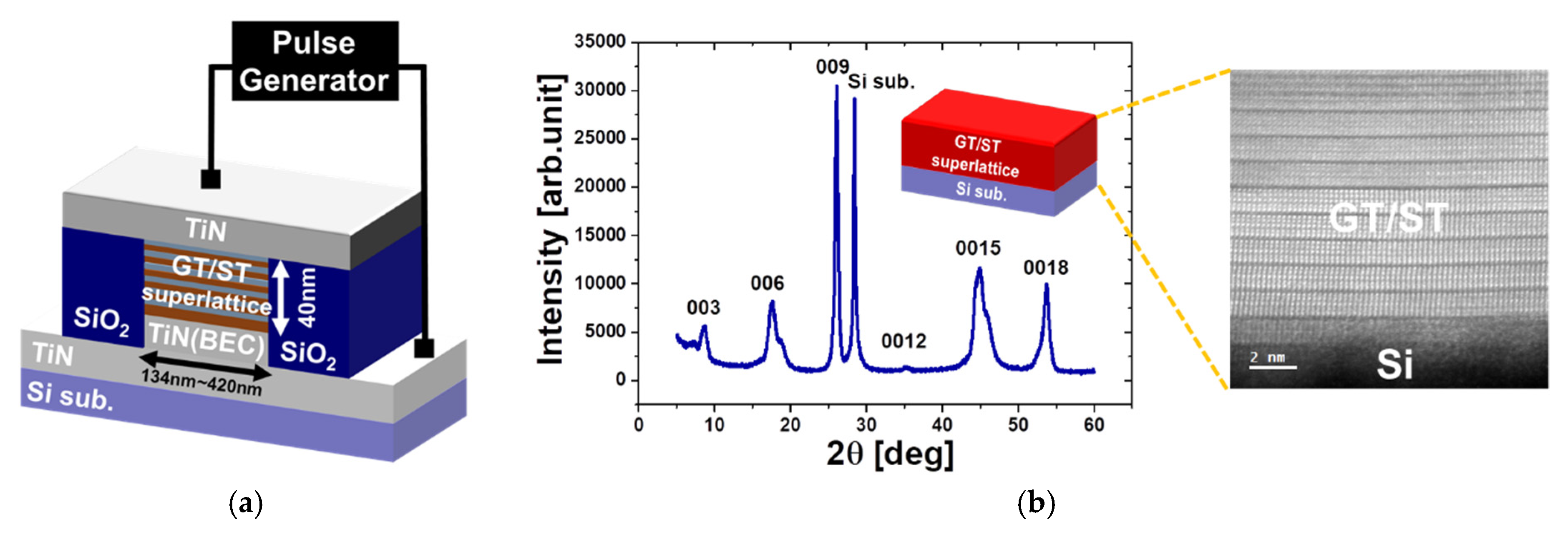
We fabricated GeTe/Sb2Te3 (GT/ST) iPCM and GST alloy samples as follows. To establish a SiO2/TiN/Si stack substrate as illustrated in Figure 1a, a SiO2 film 50 nm in thickness was deposited by chemical vapor deposition (CVD) on a TiN layer, which was deposited on an Si wafer with a (111) orientation. Next, a nano-hole with a diameter of 134 to 420 nm was patterned by photolithography and dry etching. Then, a plug of TiN that served as the bottom electrode contact (BEC) in the nano-hole was fabricated by deposition of a TiN film 50 nm in thickness combined with continuous chemical and mechanical polishing.
As previously mentioned, GT/ST iPCM operates in a crystalline state, so it is important to produce a highly-oriented superlattice structure with GeTe and Sb2Te3 layers. Therefore, a seed layer of amorphous Sb2Te3 8 nm was deposited at room temperature. To crystallize the seed layer, it was annealed at 230 °C, at which Sb2Te3 has a hexagonal structure. The seed layer becomes a crystallization template allowing for subsequent layers to grow highly oriented [16]. Then, GeTe/Sb2Te3 was alternately deposited eight times with a thickness of 1 or 3 nm, respectively, at 230 °C. After deposition, the GeTe/Sb2Te3 film was kept in a crystalline state with an in situ annealing temperature of 230 °C. All the previous Sb2Te3/GeTe layer deposition processes were performed with molecular beam epitaxy (MBE). Lastly, a TiN layer was deposited, which served as a top electrode contact. Figure 1b shows the X-ray diffraction (XRD) result and cross-sectional transmission electron microscopy (TEM)image of an MBE-grown GeTe/Sb2Te3 heterostructure.
The XRD diffraction pattern showed a relatively high peak in the (00L) direction, confirming the existence of the highly-oriented structure of the GeTe/Sb2Te3 superlattice. This result was similar to [17,18]. The periodic nature of the GT/ST layers and the van der Waals gap can be clearly seen in Figure 1b. However, the chalcogenide superlattice structure used in the iPCM device samples inevitably has imperfections (grain boundaries, dislocations, and other defects). On the other hand, the origin of the iPCM is essentially important in that each GeTe/Sb2Te3 layer in the superlattice structure forms crystalline phases. The crystallinity of each layer is a basic characteristic of the superlattice structure, and such properties displayed faster switching and lower reset energy than conventional GST samples by limiting the movement of atoms. For comparison, Ge2Sb2Te5 was manufactured with the same bottom electrode size as iPCM. To measure the IV characteristics and conductance values of the samples, a Keithley 4200A-SCS parameter analyzer (Beaverton, OR, USA) was used.
3. Experimental Results and Discussion
Before investigating the gradual conductance characteristics of GT/ST iPCM, the basic R–V switching characteristics were compared with the GST alloy. As shown in Figure 2a, it was confirmed that both the GST alloy and GT/ST iPCM operate with unipolar switching. In the case of GT/ST iPCM, it can be inferred that the shorter the pulse width time (PW), the smaller the on/off ratio of the resistance. Additionally, a higher probability of intermediate resistance states exist, as illustrated in the yellow box in Figure 2a. This is because the mechanism of the set and reset process is significantly different. On the other hand, in the case of the GT/ST iPCM samples, while maintaining the crystalline state, the movement or diffusion of Ge atoms changes resistance. This process is caused by the charge injection which activation energy required for Ge atoms to move to a specific arrangement. Therefore, it can be inferred that the dynamic range may be relatively small because the amount of Ge atoms that can transition is limited as the pulse goes toward the short pulse. This characteristic is almost identical in the GT/ST iPCM samples and in good agreement with existing iPCM research [14]. In the case of the GST alloy, on the other hand, since it operates on a melting quenching mechanism, there was no change in the resistance on/off ratio according to PW [19]. Therefore, it may be reasonable to suppose that the nature of the mechanism between GT/ST iPCM and the GST alloy behaves differently.
Figure 2b shows the change in the reset energy by the bottom electrode contact size. The reset energy was calculated at the point (the black circle in the R–V graph in Figure 2b), where the resistance reached a high resistance state when the samples were applied with an identical pulse set. Equation (1) was used to find the quantitative reset energy. The R is the resistance value at the moment of the reset operation, the V is the voltage value and the t is the applied pulse time. Although both the GST alloy and GT/ST iPCM have similar electrical behavior, where the reset energy decreases according to the bottom electrode contact size, the reset energy was significantly lower in GT/ST iPCM. As detailed in Table 1, an extreme reduction in the reset energy occurred from 69% to 83% when compared with the same bottom electrode size of the GST alloy. Hence, this result also suggests that the GST alloy and GT/ST iPCM have a different mechanism. From this data, it can be inferred that GT/ST iPCM with low power consumption is a better candidate for neuromorphic computing as it emulated more than 1010 artificial synaptic devices.
The main goal of this experiment was to demonstrate that a gradual and symmetrical conductance transition for an artificial synapse of GT/ST iPCM is achievable. Practically, biological synapses interact by conductivity called synaptic weights to update or memorize information [20,21,22]. Depending on the hardware neural network learning algorithm, the synaptic weight is given by the conductance values in the artificial synapse. The synaptic weight should increase or decrease linearly as the spike pulses are applied. This increase and decrease in the conductance values is referred to as its LTP and LTD, respectively [22]. Even though various characteristics such as the dynamic range and many conductance states are also required, we focused on the linearity and symmetry of the LTP/LTD that can control the synaptic weights with a voltage-based electrical pulse scheme. Figure 3a, illustrates a schematic of the GST alloy and GT/ST iPCM samples under different pulse conditions based on operating mechanisms. In the case of the GST alloy, a pulse scheme was designed to decrease by 0.05 V from 2 to 0.5 V with a fixed 3 μs width time for the annealing process in the set operation (=LTP). In the reset operation (=LTD), it was necessary to melt and quench with a fast and large amplitude pulse; therefore, the pulse scheme was designed to increase by 0.05 V from 2.5 to 4 V with a fixed 70 ns pulse width time.
On the other hand, GT/ST iPCM should be designed in a pulse scheme quite different from the GST alloy. A relatively short pulse and low-amplitude pulsed scheme are applied to samples for achieving gradual LTP and LTD because the switching mechanism of iPCM recognized that conductance can be tuned even with a relatively small activation energy. According to Mitrofanov et al. [19], research on the structure of the GeTe layer in iPCM revealed that four types of structure are possible depending on the temperature. These structures are mixed or predominantly distributed in the GeTe/Sb2Te3 superlattice structure. The activation energy barrier for the transition between these structures is different because the strain energy varies according to the structural transition pathways and the transition states of the possible elementary processes. However, it should be noted that the difference in the activation energy between the GeTe layer structures is a small quantity (≈2.56 eV) [23]. In addition, the process of changing the GeTe structure state is not generated in bulk but is instead diffuse according to the charge injection or electric field [12]. Therefore, a pulse scheme for LTP/LTD of iPCM was designed with a relative simplicity. In Figure 3a, the voltage amplitude applied to LTD is slightly larger than that of LTP because the activation energy that requires for structural changes between the reset and set state is different.
The model for the interaction potential based on structural transition of iPCM is illustrated in Figure 3a. There is still a debate on the mechanism of operation related to iPCM as mentioned earlier, though it is common that Ge atoms play a key role in a GeTe/Sb2Te3 superlattice with a vdW gap heterostructure. Hence, as we can see in Figure 3b, when applying the required activation energy (=Ea,Set, Ea,Reset) in the crystalline state for the reset/set operation of Ge atoms, the resistance or conductance can be tuned due to shift of the Ge diffusion in the GeTe layer structure. This suggests that the degree of Ge diffusion can be controlled by electrical pulses; however, measuring the exact amount of diffusion may be future research work.
Based on the assumption for a pulse scheme that can achieve gradual and symmetrical LTP/LTD, the results of the GST alloy and GT/ST samples are depicted in Figure 4a to Figure 4d, respectively. As shown in Figure 4a, it appears that the LTP/LTD of the GST alloy shifted abruptly. On the other hand, the GT/ST iPCM resulted in a gradual increase and decrease in synaptic weight and high symmetrical LTP/LTD. This disparity is because melting and annealing produce bulk in the case of a GST alloy, leading to a high probability in sharp shifts in conductance values. GT/ST iPCM samples, which operate on atomic reconfiguration by electric field, produced gradual and symmetric tuning. It seems that the amount of diffusion of the Ge atoms can be properly regulated in the pulse amplitude range 0.6–1.0 V for the optimum LTP. Furthermore, the LTD most gradually decreases in the 1.2 V pulse scheme in the GT/ST iPCM samples. When it is lower than 0.6 V, a transition hardly occurs, and it can be predicted that the Ge atoms do not have enough energy to cross Ea,Set. When it is larger than 1.2 V, it is predicted that the conductance values rapidly change, as avalanche diffusion of Ge atoms occurs.
The quantitative measurements of calculated non-linearity (NL) and symmetry for artificial synapse application are listed in Table 2. The non-linearity calculation is a measure of the error of a line that is linearly drawn based on the maximum (Gmax) and minimum (Gmin) values of the synaptic weight. In the symmetry calculation, the amount of change in the synaptic weight per spike in the process of LTP and LTD is calculated, respectively. Then, the percentage of synaptic weight coidentity is calculated and averaged, and the following Equation (2) is obtained. If the synaptic weight change of LTP is larger than LTD, it is calculated by changing the denominator and numerator of Equation (2).
When the amplitude values of LTP/LTD were 0.6 V/1.2 V and 70 ns, the symmetry with 90.6% was produced and is 63% improved compared to GST alloy. However, NL became worse at 0.6 V/1.2 V because the original LTD at 1.2 V was 2.10 to 2.56. In other words, there is a tradeoff between symmetry and NL in a GT/ST iPCM sample. However, the fact that the number of spikes operating LTP/LTD is equal to 30 spikes and that the pulse scheme operates while consuming very low voltage suggests that it can be expected to be a great advantage as an artificial synapse.
4. Conclusions
In this study, we have fabricated an iPCM superlattice heterostructure based on GeTe/Sb2Te3, and it can be applied to a wide range of designs for a superlattice structure using 2D materials. Furthermore, it was shown that the reset energy consumption is reduced by more than 69% compared to the GST alloy. The intermediate states are also verified with a short pulse in unipolar switching to confirm the possibility of operation with an artificial synapse operating at low energy by BEC size. The process of Ge diffusion by GT/ST iPCM was modeled from the fact that the GeTe structures transit with activation energy. As a result, gradual and symmetry conductance can be achieved in LTP/LTD by the optimal electrical pulse scheme. Our results reached 90.6% symmetry and relatively low NL (<3) by applying the identical spikes of 70 ns at 0.6 V/1.2 V to LTP/LTD. Future work should focus on improving the NL of LTD because it is more sensitive than increasing the synaptic weight in the LTP process. In this regard, the gradual and symmetry conductance tuning method of GeTe/Sb2Te3 iPCM according to the voltage-based pulse scheme will be essential as an artificial synaptic device to be utilized in hardware neural networks with high performance.
Author Contributions
Conceptualization, S.K.; methodology, S.K. and J.L.; investigation, S.K.; writing—original draft preparation, S.K.; writing—review and editing, S.K., J.L. and Y.S.; visualization, S.K.; supervision, Y.S. and M.K.; funding acquisition, M.K. All authors have read and agreed to the published version of the manuscript.
Funding
This research was supported by the Ministry of Trade, Industry & Energy (MOTIE) (project number 10080625) and the Korea Semiconductor Research Consortium (KSRC) support program for the development of future semiconductor devices.
Conflicts of Interest
The authors declare no conflict of interest.
References
- Von Neumann, J. First Draft of a Report on the EDVAC. IEEE Ann. Hist. Comput. 1993, 15, 27–75. [Google Scholar] [CrossRef]
- Kuzum, D.; Yu, S.; Wong, H.S.P. Synaptic electronics: Materials, devices and applications. Nanotechnology 2013, 24, 382001. [Google Scholar] [CrossRef]
- Islam, R.; Li, H.; Chen, P.Y.; Wan, W.; Chen, H.Y.; Gao, B.; Wong, H.P. Device and materials requirements for neuromorphic computing. J. Phys. D Appl. Phys. 2019, 52, 113001. [Google Scholar] [CrossRef]
- Kuzum, D.; Jeyasingh, R.G.D.; Lee, B.; Wong, H.S.P. Nanoelectronic programmable synapses based on phase change materials for brain-inspired computing. Nano Lett. 2011, 12, 2179–2186. [Google Scholar]
- Suri, M.; Bichler, O.; Querlioz, D.; Cueto, O.; Perniola, L.; Sousa, V.; Vuillaume, D.; Gamrat, C.; DeSalvo, B. Phase change memory as synapse for ultra-dense neuromorphic systems: Application to complex visual pattern extraction. IEEE Int. Electron. Devices Meet. (IEDM) 2011. [Google Scholar] [CrossRef]
- Kuzum, D.; Jeyasingh, R.G.D.; Wong, H.S.P. Energy efficient programming of nanoelectronic synaptic devices for large-scale implementation of associative and temporal sequence learning. IEEE Int. Electron. Devices Meet. (IEDM) 2011. [Google Scholar] [CrossRef]
- Lankhorst, M.; Ketelaars, B.; Wolters, R. Low-cost and nanoscale non-volatile memory concept for future silicon chips. Nat. Mater. 2005, 4, 347–352. [Google Scholar] [CrossRef]
- Xu, K. Integrated silicon directly modulated light source using p-well in standard CMOS technology. IEEE Sens. J. 2016, 16, 6184–6191. [Google Scholar] [CrossRef]
- Wong, H.-S.P.; Raoux, S.; Kim, S.; Liang, J.; Reifenberg, J.P.; Rajendran, B.; Asheghi, M.; Goodson, K.E. Phase change memory. Proc. IEEE. 2010, 98, 2201–2227. [Google Scholar] [CrossRef]
- Simpson, R.E.; Fons, P.; Kolobov, A.V.; Fukaya, T.; Krbal, M.; Yagi, T.; Tominaga, J. Interfacial phase-change memory. Nat. Nanotechnol. 2011, 6, 501–505. [Google Scholar]
- Yu, X.Y.; Chen, G.; Verma, A.; Smith, J.S. Temperature dependence of thermophysical properties of GaAs/AlAs periodic structure. Appl. Phys. Lett. 1995, 67, 3554–3556. [Google Scholar] [CrossRef]
- Egami, T.; Johguchi, K.; Yamazaki, S.; Takeuchi, K. Investigation of multi-level-cell and set operations on super-lattice phase change memories. Jpn. J. Appl. Phys. 2014, 53, 04ED02. [Google Scholar] [CrossRef]
- Xiaoming, Y.; Robertson, J. Modeling of switching mechanism in GeSbTe chalcogenide superlattices. Sci. Rep. 2015, 5, 12612. [Google Scholar]
- Chew, K.H.; Zhou, Y.; Ong, L.H.; Iwata, M. A dipole lattice model of switching characteristics in ferroelectric superlattices. J. Appl. Phys. 2013, 114, 224108. [Google Scholar] [CrossRef] [Green Version]
- Saito, Y.; Kolobov, A.V.; Fons, P.; Mitrofanov, K.V.; Makino, K.; Tominaga, J.; Robertson, J. Origin of resistivity contrast in interfacial phase-change memory: The crucial role of Ge/Sb intermixing. Appl. Phys. Lett. 2019, 114, 132102. [Google Scholar] [CrossRef]
- Saito, Y.; Mitrofanov, K.V.; Makino, K.; Miyata, N.; Fons, P.; Kolobov, A.V.; Tominaga, J. Sputter Growth of Chalcogenide Superlattice Films for Future Phase Change Memory Applications. ECS Trans. 2018, 86, 49. [Google Scholar] [CrossRef]
- Mitrofanov, K.V.; Saito, Y.; Miyata, N.; Fons, P.; Kolobov, A.V.; Tominaga, J. High-speed bipolar switching of sputtered Ge–Te/Sb–Te superlattice iPCM with enhanced cyclability. Phys. Status Solidi (RRL) Rapid Res. Lett. 2019, 13, 1900105. [Google Scholar] [CrossRef]
- Xu, K.; Huang, L.; Zhang, Z.; Zhao, J.; Zhang, Z.; Snyman, L.W.; Swart, J.W. Light emission from a poly-silicon device with carrier injection engineering. Mater. Sci. Eng. B 2018, 231, 28–31. [Google Scholar] [CrossRef]
- Mitrofanov, K.V.; Saito, Y.; Miyata, N.; Fons, P.; Kolobov, A.V.; Tominaga, J. Resistive switching characteristics of interfacial phase-change memory at elevated temperature. Jpn. J. Appl. Phys. 2018, 57, 04FE06. [Google Scholar] [CrossRef]
- Yu, S. Neuro-inspired computing with emerging nonvolatile memory. Proc. IEEE 2018, 106, 260–285. [Google Scholar] [CrossRef]
- Burr, G.W.; Shelby, R.M.; Sebastian, A.; Kim, S.; Kim, S.; Sidler, S.; Sanches, L.L. Neuromorphic computing using non-volatile memory. Adv. Phys. X 2017, 2, 89–124. [Google Scholar] [CrossRef]
- Haensch, W. Analog Computing for Deep Learning: Algorithms, Materials & Architectures. IEEE Int. Electron. Devices Meet. (IEDM) 2018. [Google Scholar] [CrossRef]
- Nobuki, I.; Nakamura, H. Structural transition pathway and bipolar switching of the GeTe–Sb2Te3 superlattice as interfacial phase-change memory. Faraday Discuss. 2019, 213, 303–319. [Google Scholar]
Figure 1.
(a) Schematic of the fabricated GeTe/Sb2Te3 (GT/ST) interfacial phase-change memory (iPCM) structure, (b) XRD diffraction pattern of a GT/ST SL (SL) structure and cross-sectional TEM image of the GT/ST superlattice on an Si (111) substrate.
Figure 1.
(a) Schematic of the fabricated GeTe/Sb2Te3 (GT/ST) interfacial phase-change memory (iPCM) structure, (b) XRD diffraction pattern of a GT/ST SL (SL) structure and cross-sectional TEM image of the GT/ST superlattice on an Si (111) substrate.

Figure 2.
(a) A R–V graph of the GT/ST iPCM and Ge–Sb–Te (GST) alloy by the pulse width time, (b) a comparison graph of the reset energy by the bottom electrode contact (BEC) size (134, 218, 420 nm) between the GT/ST iPCM and GST alloy. The R–V graph in the figure shows the reset operation for each BEC size.

Figure 3.
(a) Pulse scheme for long-term potentiation (LTP)/long-term depression (LTD) considering the mechanism of the GST alloy and GT/ST iPCM. (b) Schematic of the potential for Ge atoms of iPCM to diffuse in the reset and set states. The Ge atoms are shown in blue, Te atoms in yellow, and Sb atoms in orange.

Figure 4.
Long-term potentiation and depression of the GST alloy and GT/ST iPCM. (a) A total of 28 spikes were used for potentiation, and 33 spikes were used for depression. (b) LTP: 11 spikes (70 ns, 1 V); LTD: 30 spikes (70 ns, 1.2 V). (c) LTP: 19 spikes (70 ns, 0.8 V); LTD: 30 spikes (70 ns, 1.2 V). (d) LTP: 30 spikes (70 ns, 0.6 V); LTD: 30 spikes (70 ns, 1.2 V).


Table 1.
Reduction amount of the reset energy by BEC size.
| BEC (nm) | 134 | 218 | 420 |
| Energy reduction | 69% | 81% | 83% |
Table 2.
Symmetry and non-linearity (NL) of the GST alloy and GT/ST iPCM samples.
| (a) | (b) | (c) | (d) | |
|---|---|---|---|---|
| Symmetry | 27.4% | 38.6% | 55.0% | 90.6% |
| NL (LTP/LTD) | 1.22/0.94 | 0.32/2.56 | 0.91/2.10 | 1.97/2.56 |
© 2020 by the authors. Licensee MDPI, Basel, Switzerland. This article is an open access article distributed under the terms and conditions of the Creative Commons Attribution (CC BY) license (http://creativecommons.org/licenses/by/4.0/).
Share and Cite
MDPI and ACS Style
Kang, S.; Lee, J.; Kang, M.; Song, Y. Achievement of Gradual Conductance Characteristics Based on Interfacial Phase-Change Memory for Artificial Synapse Applications. Electronics 2020, 9, 1268. https://doi.org/10.3390/electronics9081268
AMA Style
Kang S, Lee J, Kang M, Song Y. Achievement of Gradual Conductance Characteristics Based on Interfacial Phase-Change Memory for Artificial Synapse Applications. Electronics. 2020; 9(8):1268. https://doi.org/10.3390/electronics9081268
Chicago/Turabian StyleKang, Shinyoung, Juyoung Lee, Myounggon Kang, and Yunheub Song. 2020. "Achievement of Gradual Conductance Characteristics Based on Interfacial Phase-Change Memory for Artificial Synapse Applications" Electronics 9, no. 8: 1268. https://doi.org/10.3390/electronics9081268
Note that from the first issue of 2016, this journal uses article numbers instead of page numbers. See further details here.